Article

Reference-Free Dynamic Voltage Scaler Based on Swapping Switched-Capacitors

1
Department of Electronic Engineering, College of Electrical Engineering and Computer Science, Chungbuk National University, Cheongju-si 28644, Korea
2
Department of Electronic, National Telecommunication Institute, Nasr City, Cairo 11768, Egypt
*
Authors to whom correspondence should be addressed.
Energies 2019, 12(4), 625; https://doi.org/10.3390/en12040625
Submission received: 14 December 2018 / Revised: 12 February 2019 / Accepted: 13 February 2019 / Published: 15 February 2019
(This article belongs to the Special Issue Advanced Techniques for Electronic Power and Energy Systems)

Abstract

:
This paper introduces a reference-free, scalable, and energy-efficient dynamic voltage scaler (DVS) that can be reconfigured for multiple outputs. The proposed DVS employs a novel swapping switched-capacitor (SSC) technique, which can generate target output voltages with higher resolution and smaller ripple voltages than the conventional voltage scalers based on switched-capacitors. The proposed DVS consists of a cascaded 2:1 converter based on swapping capacitors, which is essential to achieve both very small voltage ripple and fine-grain conversion ratios. One of the serious drawbacks of the conventional voltage scalers is the need for external reference voltages to maintain the target output voltage. The proposed SSC; however, eliminates the needs for any reference voltages. This significant benefit is achieved by the self-charging ability of the SSC, which can recharge all its capacitors to the configured voltage by simply swapping the two capacitors in each stage. The proposed SSC-DVS was designed with a resolution of 16 output levels and implemented using a 130 nm CMOS (Complementary Metal Oxide semiconductor) process. We conducted measured results and post-layout simulations with an input voltage of 1.5 V to produce an output voltage range of 0.085–1.4 V, which demonstrated a power efficiency of 85% for a load current of 550 µA with a voltage ripple of as low as 2.656 mV for a 2 KΩ resistor load.

1. Introduction

Voltage converters are essential building blocks for many low power devices, such as biomedical devices, mobile phones, wireless sensor networks, energy harvesting devices, and internet-of-things (IoT) devices [1,2,3,4,5,6].
Nowadays, switched-capacitor voltage converters are the most popular architectures due to their process compatibility, high efficiency, and small area when integrated on-chip. Although inductor-based DC-DC converters have been commonly used in classical applications, they almost always require off-chip inductors, which makes them unsuitable for on-chip voltage scalers supplying multiple power domains. Implementing on-chip inductors incurs excessive chip areas for present process technologies. It also requires a special process to achieve an on-chip inductor with a high-quality factor, which increases both the complexity and the cost.
C. Huang et al. [7] demonstrated effective methods that can improve the quality factor of the inductor based on a packaged bond-wire-based inductive converter. This approach; however, requires special bonding wires that makes its fabrication impractical. On the other hand, conventional voltage converters based on switched-capacitors offer energy efficiency with only limited switching frequency and specific output voltages. Operating such voltage converters in non-optimal conditions often result in significant degradation in their energy efficiency. Moreover, to add more conversion ratios to switched-capacitor (SC) voltage converters, like a series-parallel SC converter, often increases the design complexity and the area of capacitor array while degrading the efficiency [8,9,10,11,12,13].
Loai G. Salem et al. [14] presented a voltage converter based on recursive switched-capacitor topology. It achieves 2n conversion ratios with a peak efficiency of 85.8%. This architecture; however, requires an excessive number of switches. In addition, the number of control signals increases, thus the complexity of the controller increases as well. Moreover, it needs extra bias voltage and a reference voltage, which requires additional circuits. Moreover, the reported architecture does not offer the scalability, which is important for DVS. In other words, if we need to change the target voltage or increase the number of voltage levels, we must redesign the whole circuit.
Switched-capacitor down-converters and up-converters based on the self-oscillation technique have been reported by [4,15,16]. To generate just one conversion ratio of 1:2 or 2:1, they implement an odd number of stages, usually more than three stages, with a delay circuit added between every two stages. Therefore, they require a large number of switches; in addition, they add two capacitors for each stage, leading to an area increment. They also do not offer the reconfigurability, which is required for DVS. Suyoung Bang et al. [9] reported a voltage converter based on the SAR (Succcessive Approximation Switched-capacitor) structure. It provides 2n ratios with a peak efficiency of 72%. This architecture; however, suffers from the cascaded losses, in which some stages take the charges only from the previous stage, not from the supply voltage, so such losses are unavoidable in this architecture. It also requires a comparator and a reference voltage generator. To provide the reference voltage; thus, they implemented a voltage regulator based on 2n diodes formed by connecting PFETs (P-channel Field Effect Transistors) in series. This makes the voltage regulator become excessively complex as N increases, in addition to the growing overhead of the configuration switches.
A soft-charging SC voltage converter is presented in [17]. It employs stage out-phasing and multi-phase soft-charging approaches. They can reduce the energy loss caused by charge-sharing, provide better capacitance utilization, and higher efficiency. It; however, divides each stage into m sub-stages with extra phase control signals. This leads to excessive design complexity and poor energy efficiency for a large number of sub-stages.
To resolve the problems of the previous converters discussed above, this paper presents a dynamic voltage scaler (DVS) based on cascaded, swapping switched-capacitors (SSCs). It provides high-resolution outputs, high power efficiency, and low voltage ripples. It also allows a wide-range input voltage, while concurrently producing multiple outputs with fine-grain steps. The proposed architecture provides a wide-range of conversion ratios (CRs). For an SSC with n stages, it produces 2n steps with a voltage resolution of Vin/2n. The essential component of the proposed DVS is the swapping capacitor stage with a 2:1 voltage ratio. It maintains the output voltage by periodically swapping the upper and bottom capacitors in each stage, which ensures that the bottom capacitor is always charged to the target voltage.
This paper is organized as follows: Section 2 presents the architecture of the proposed DVS based on cascaded SSCs. Section 3 provides analytic models of the output voltage, current flow, and steady-state energy efficiency of the proposed SSC-DVS. Section 4 demonstrates the simulation experiment results of the proposed circuit. Finally, Section 5 highlights the key contributions of this work.

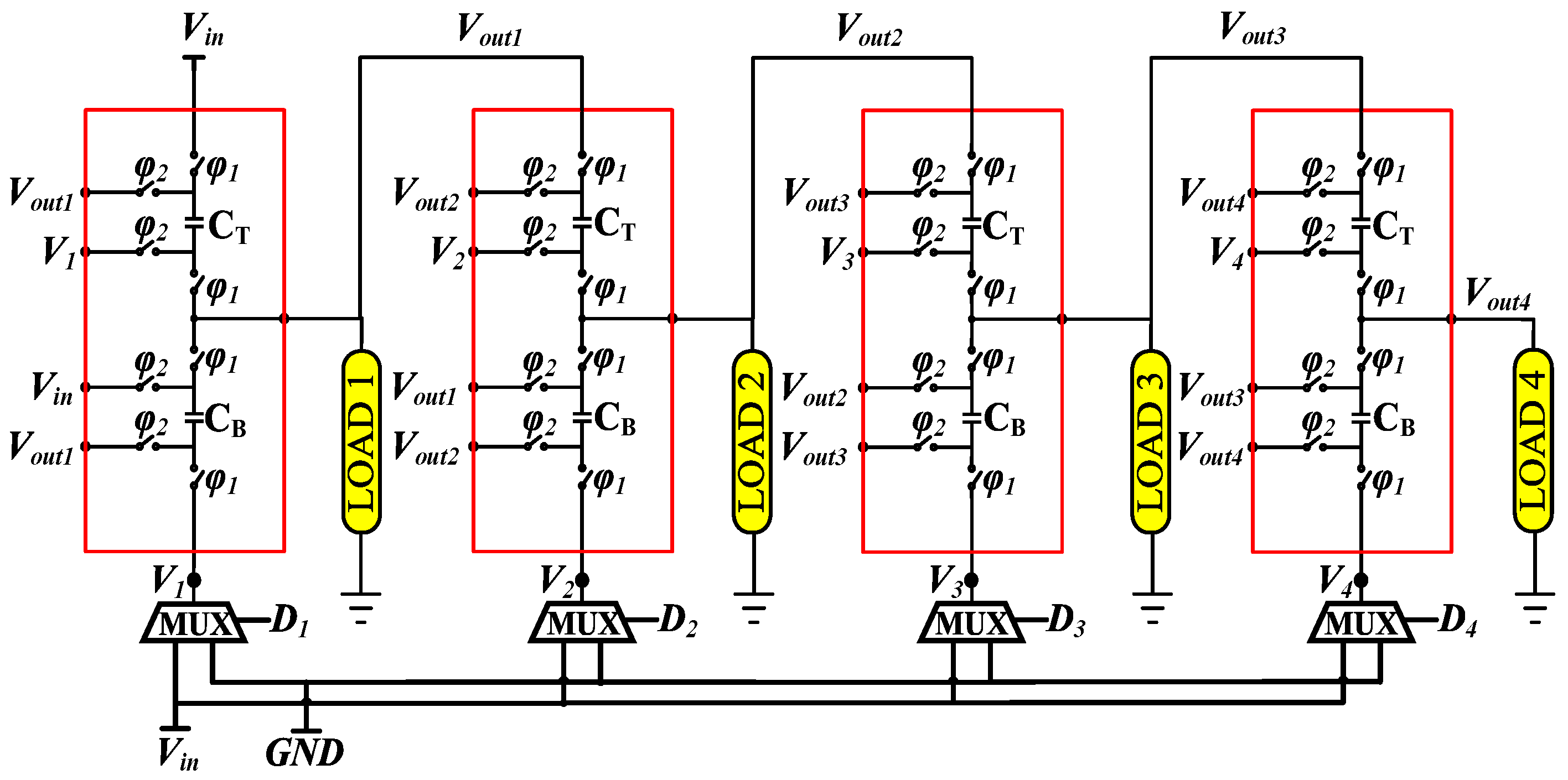
2. The Architecture of the Swapping Switched-Capacitor-Based DVS

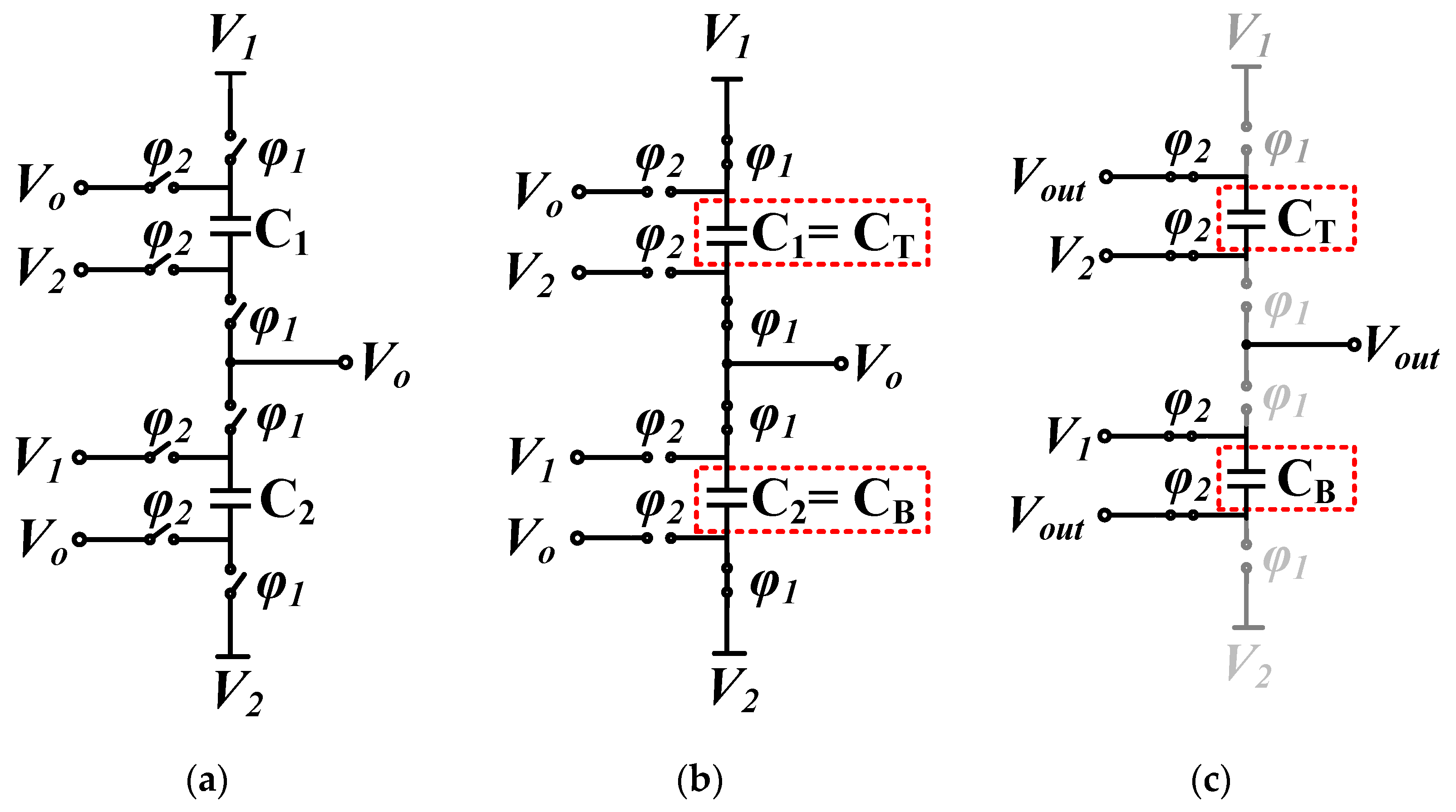
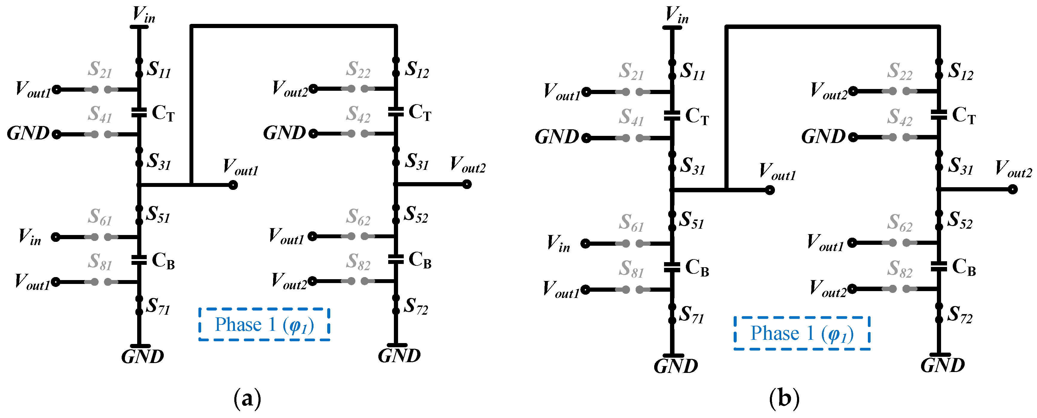
2.1. Circuit Operation

Figure 1 shows the structure of each stage of the proposed SSC. It consists of two equal-sized capacitors and eight switches. The capacitors work as a voltage divider to generate the average of the two inputs, while the switches are used to swap the two capacitors’ positions. By swapping the capacitors faster than the changes in their voltage, the capacitors can maintain the output voltage of each stage. The unit cell of Figure 1 operates as follows:
  • Two inputs V 1 and V 2 are applied to the SSC-DVS input ports to generate the average value V o u t = V 1 + V 2 2 .
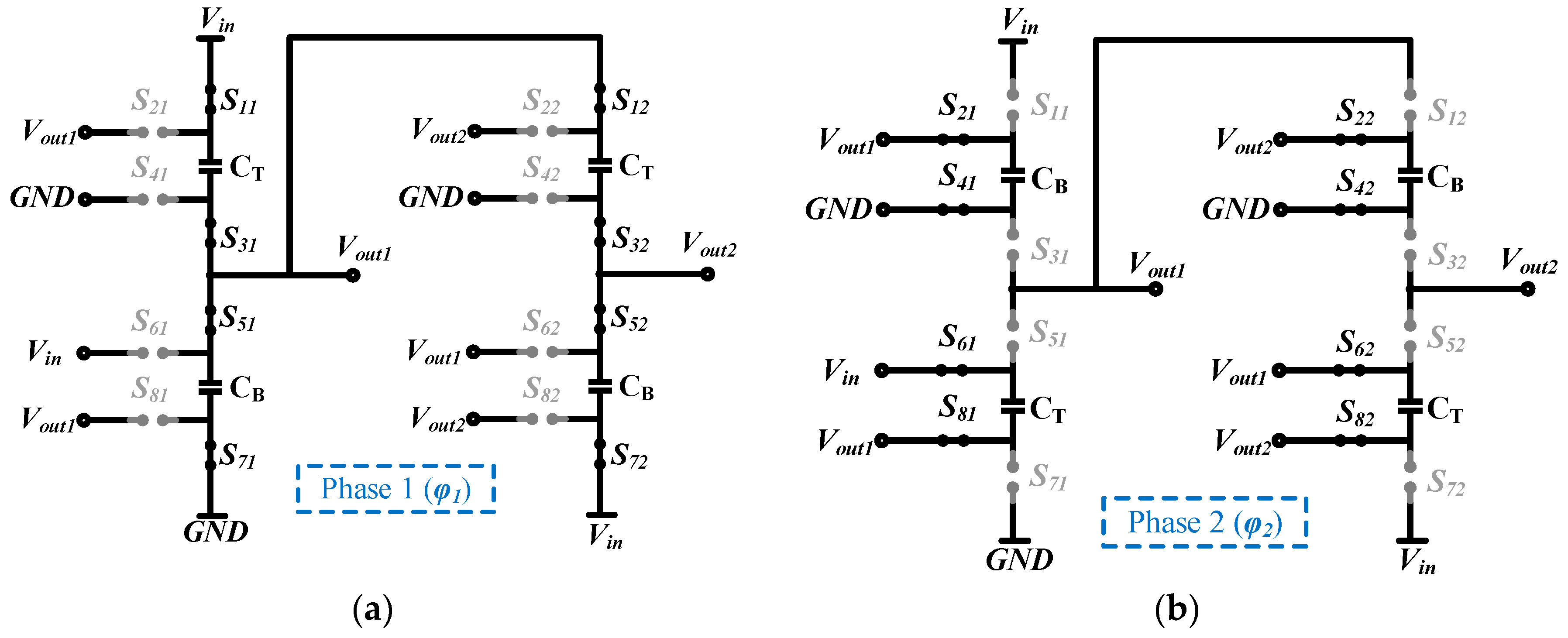
  • In phase 1, the bottom capacitor, CB, delivers the charges to the load circuit, and thus the amount of CB’s charge decreases. Therefore, the voltage across CB decreases while the voltage across CT increases over time. When at the middle of switching time ( T S 2 ) , the controller switches to phase 2.
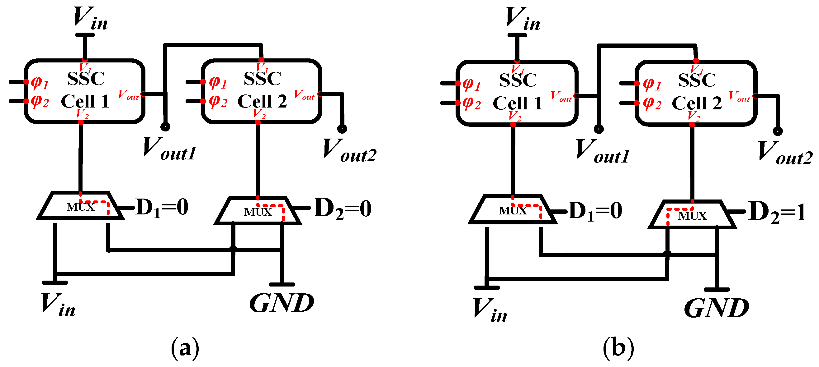
  • In phase 2, the controller reconfigures the cell by swapping CB and CT. Then CB’s positive terminal is connected to V1, while its negative terminal is connected to Vout, as illustrated by Figure 1c. On the other hand, CT’s positive terminal is connected to Vout while its negative terminal is connected to V2, as illustrated by Figure 1c.
  • In phase 2, CT supplies the load.
  • When TS, the controller switches back to phase 1, and the above steps are repeated.

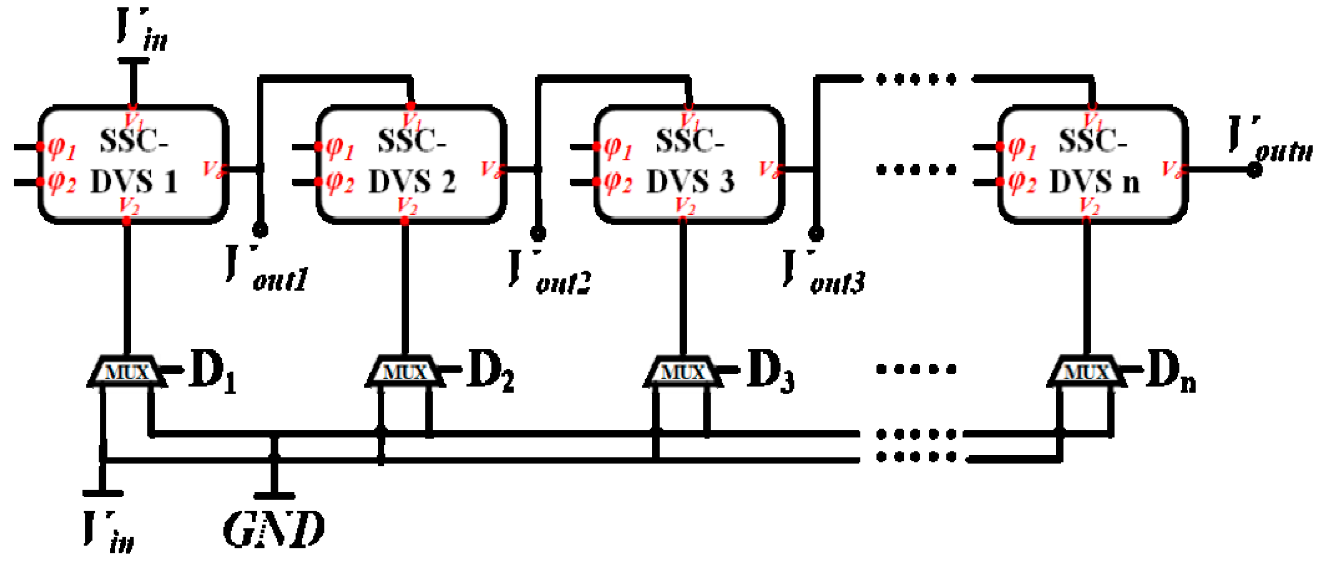
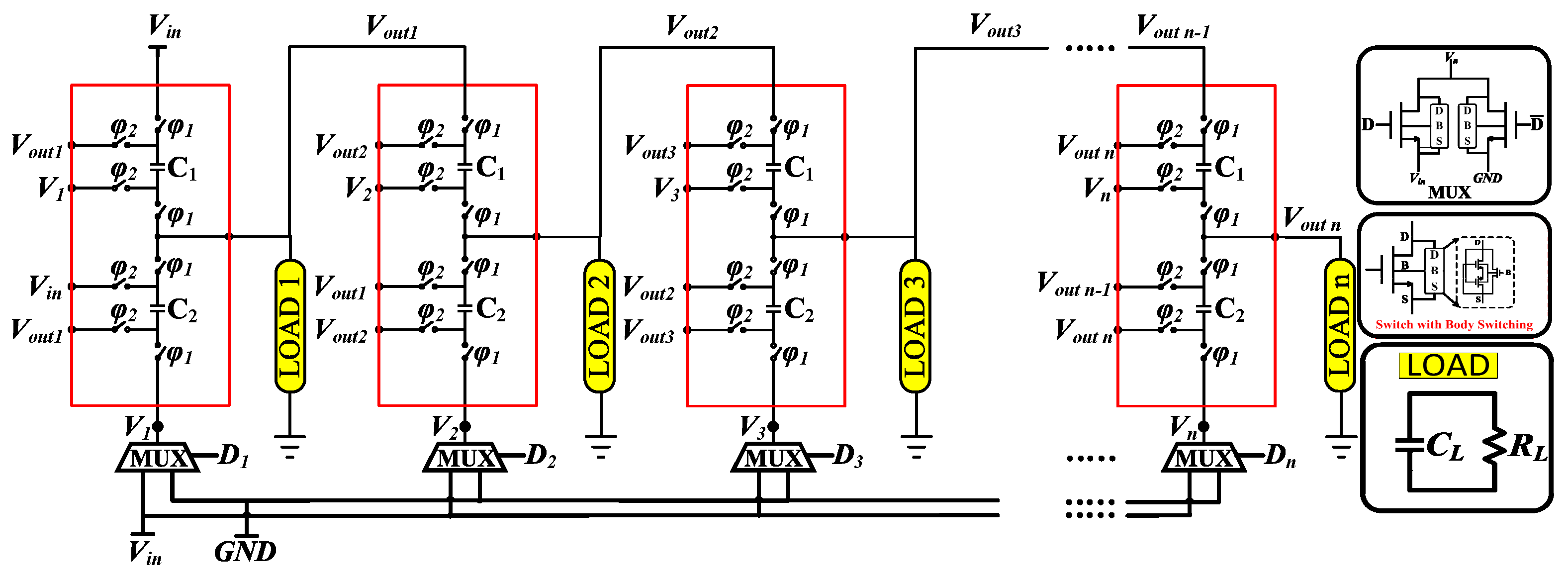
2.2. SSC-DVS Architecture

Figure 2 shows the architecture of an n-bit SSC-DVS which generates 2n levels of output voltages. Figure 3 illustrates the detailed circuit schematic of the n-bit SSC-DVS.
To quantify the proposed SSC-DVS, the SSC-DVS was implemented using metal–insulator–metal (MIM) capacitors. We chose MIM capacitors because they provide a relatively large capacitance for unit space and usually exhibit acceptable process variation. The other integrated capacitors, such as poly–insulator–poly (PIP) or metal–oxide–metal (MOM) structures, in contrast, exhibit more parasitic than MIMs [18,19].
Figure 4 illustrates the transmission gate structure of the switches that were used in the implemented circuit. The transmission gate consisted of NMOS (N-type Metal Oxide Semiconductor) and PMOS (P-type Metal Oxide Semiconductor) devices, and their body switches. The body switches can reduce the leakage current using the body switching technique [20,21]. The aspect ratio of the transmission-gate transistors were ( W L ) n = ( W L ) p = 20   μ m 0.13   μ m , which were selected based on the maximum target output current, while the aspect ratio of the body switch transistors were ( W L ) p 1 = ( W L ) p 2 = 0.15   μ m 0.13   μ m .
Figure 5a depicts a small example of n = 2 when the target voltages were Vout1 = 750 mV and Vout2 = 375 mV. To explain the operation of the proposed architecture: In phase 1 (φ1) in Figure 6a, the vertical switches in stage 1 (S11, S31, S51, and S71) and stage 2 (S12, S32, S52, and S72) were ON; while the horizontal switches in stage 1(S21, S41, S61, and S81) and stage 2 (S22, S42, S62, and S82) were OFF. In phase 2 (φ2) in Figure 6b, the vertical switches were OFF and the horizontal switches were ON.
To generate, for example, conversion ratios of 1 2 and 1 4 , we applied D1D2 = (00)2 to connect the V1 and V2 inputs of the first stage to Vin and GND, respectively, leading to V o u t 1 = V i n + G N D 2 = 1 2 V i n . Then, inputs V1 and V2 of the second stage were connect to Vout1 and GND, respectively, producing V o u t 2 = V o u t 1 + G N D 2 = 0.5 V i n + G N D 2 = 1 4 V i n . Figure 6a,b show φ1 and φ2 phases, used to configure the switches of the swapping process to generate conversion ratios of 1 2 and 1 4 .
In the second configuration of Figure 7, we applied D1D2 = (01)2 to generate conversion ratios of 1 2 and 3 4 . Figure 7 shows phases φ1 and φ2 to configure the switches of the swapping process to generate conversion ratios of 1 2 and 3 4 . We connected inputs V1 and V2 of the first stage to Vin and GND, respectively, resulting in V o u t 1 = V i n + G N D 2 = 1 2 V i n . Then inputs V1 and V2 of the second stage were connected to Vout1 and Vin, respectively, giving V o u t 2 = V o u t 1 + G N D 2 = 0.5 V i n + V i n 2 = 3 4 V i n . With Vin of 1.5 V, hence, the above SSC-DVS could generate 375 and 750 mV when D1D2= (010)2, while producing 750 and 1.125 mV when D1D2 = (01)2.

3. Analytic Model

This section provides steady-state analysis for target output voltages of the proposed SSC-DVS. It also derives the current model of the proposed architecture while calculating its energy efficiency.

3.1. Steady-State Output Voltage

The output of the proposed SSC-DVS was connected in parallel with an output capacitor to reduce the voltage ripple. Table 1 shows the simulation results of the effect of the output capacitor size on the voltage ripple. Here, VRipplen corresponded to Voutn where 1 < n < 4. The voltage ripple was measured for all the four outputs of 4-bit SSC-DVS. For example, Table 1 shows that the voltage ripple gave a maximum value of 2.16 mV for CL of 500 pF, whereas it gave a minimum value of 0.199 mV for CL of 4 nF.
In phase 1 (φ1), the bottom flying capacitor CB delivered the charges to both the output capacitor and the load resistor. The n-bit SSC-DVS provided n output voltages. Each output voltage could be described by Equation (1). The conversion ratio (CR) of K output voltage could be expressed by Equation (4).
[ V o u t 1 V o u t 2 V o u t 3 V o u t n ] = [ 0 0 0 ( 1 + D 1 ) 0 0 ( 1 + D 1 ) D 2 ( 1 + D 1 ) D 2 D 3 ( 1 + D 1 ) D n 2 D n 1 D n ] × [ 1 2 n V i n 1 2 3 V i n 1 2 2 V i n 1 2 1 V i n ]
V o u t = C R × V i n
R e s o l u t i o n = V i n 2 K
C R = R e s o l u t i o n × ( 1 + B c o d e K )
Here, Voutn is the output voltage of the n stage, Dn is the digital configuration bit of n stage to select the top voltage V1 or bottom voltage V2, B c o d e K is the binary code (decimal value) which consists of K digital bits D 1 , D 2 D K (D1 is the MSB (Most Significant Bit)), and K is the number of stages in the range of 1 ≤ Kn. The following examples explain the voltage equations. A 6-bit SSC-DVS with 1.5 V input voltage generated 26 = 64 voltage levels with a voltage step of 1.5 2 6 ≈ 23.44 mV, while it generated multiple outputs up to 6 outputs simultaneously. Figure 8 shows a 6-bit SSC-DVS example with two different configurations Bcode = (010110)2 and Bcode = (001100)2. Table 2 shows the conversion ratios for the generated output voltage levels. In Figure 8, the top port of the first stage was connected to the Vin, while the bottom port was connected to GND with “0”. Hence, the Vout1 equals the average of the two inputs of the first stage leading to V o u t 1 = V i n + G N D 2 = 1.5 + 0 2 = 0.75   mV . Then, Vout1 was supplied to the top port of the second stage, while the bottom port was connected to Vin due to the second bit “1” in Bcode= (010110)2. Hence, V o u t 2 = V i n + V o u t 1 2 = 1.5 + 0.75 2 = 1.125   V . In this way, the steady-state output voltage of each stage could be determined by selecting a configuration code.

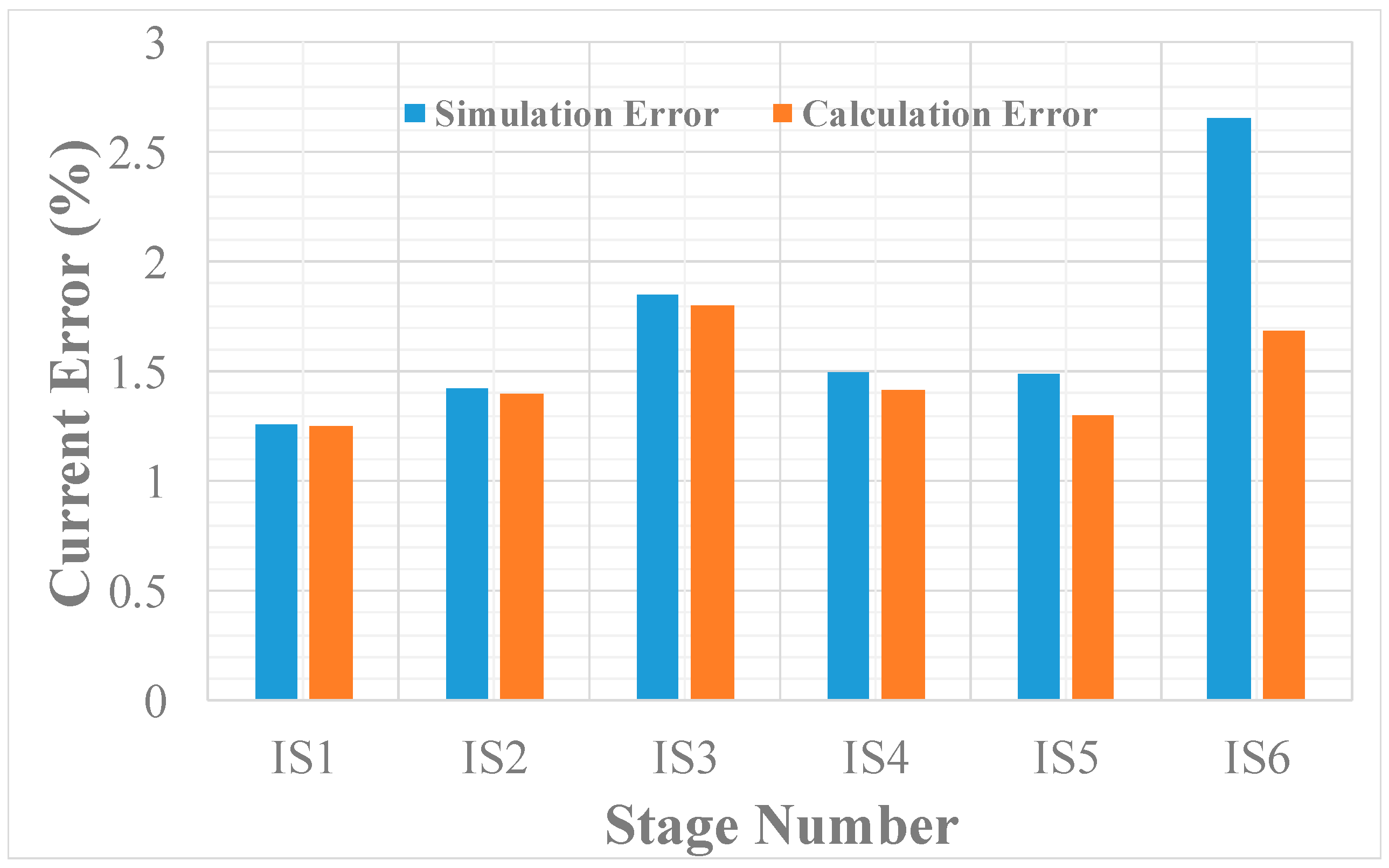
3.2. Analysis of Steady-State Current Flows in Each Stage

This subsection analyzes the current flow of SSC-DVS in two cases: A single-output case and a multi-output case.

3.2.1. SingleOutput Case

Figure 9 shows two configuration examples of a 6-bit SSC-DVS with a single-output based on two different configurations. Figure 9a,b show current paths of the SSC-DVS with Bcode= (010110)2 and Bcode = (001100)2, respectively. The conversion ratios for the two examples were CR = 27 64 and CR = 13 64 , respectively. Equation (5) describes a generalized equation of the output current at the n-th output Voutn for the proposed SSC-DVS architecture, illustrated by Figure 3.
I o u t n = I i n C R n
I o u t n = 2 n 1 + K = 1 K = n 2 K 1 D K × I i n
Here, Iin is the input current and I o u t n is the output current of the n-th stage. For the example of Figure 9a, which has Bcode= (010110)2 producing a conversion of 27 64 , each output from stage 1 to stage 6, respectively, provided 1 32 ·Iout6, 1 16 ·Iout6, 1 8 ·Iout6, 1 4 ·Iout6, 1 2 ·Iout6, and Iout6. Based on Equation (5), the total input current at the input port Vin was Iin = 27 64 ·Iout6. Here Iout6 was the output current at the final output V o u t 6 as illustrated in Figure 9a. The current Iin drawn from the Vin source could be calculated as Iin = ( 1 64 + 1 32 + 1 8 + 1 4 ) ·Iout6 by Equation (5).
In the second example given in Figure 9b, the current for each SSC stage could be calculated in the same way as the first example using Equation (5). The total current at the input port Vin was Iin = 13 64 ·Iout6, which was calculated by Equation (5) as Iin = ( 1 64 + 1 16 + 1 8 ) ·Iout6.

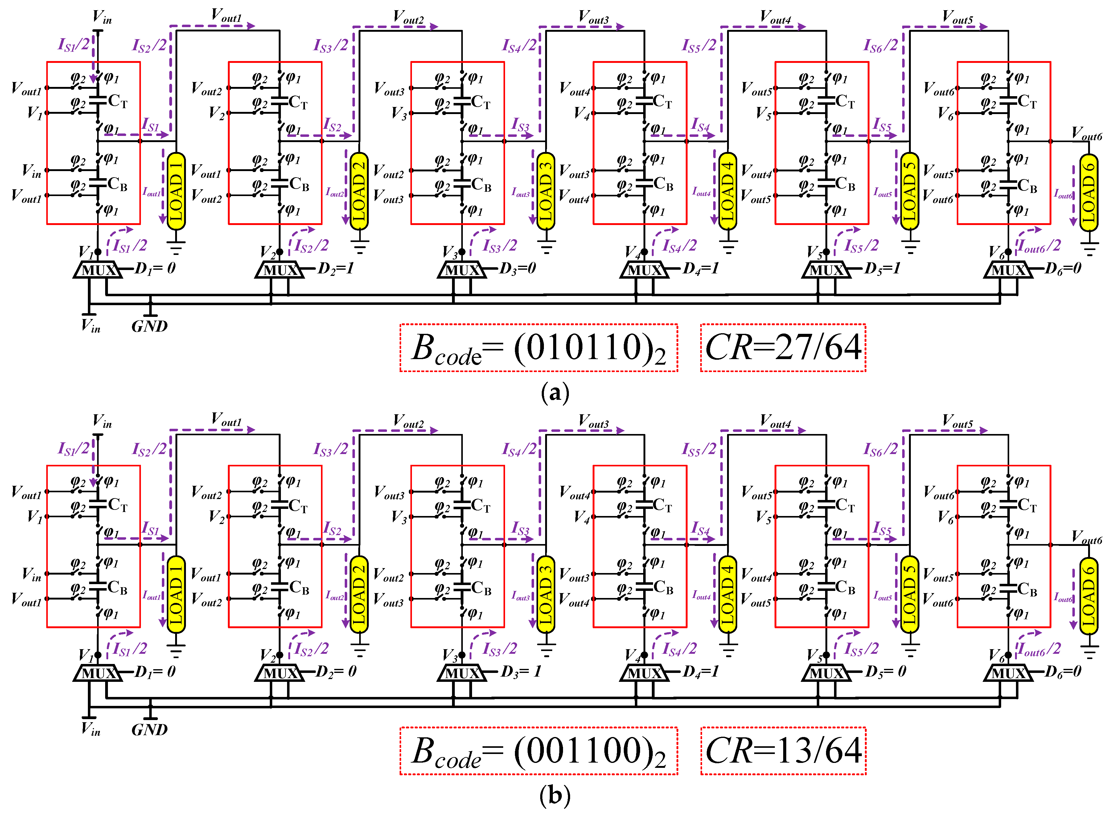
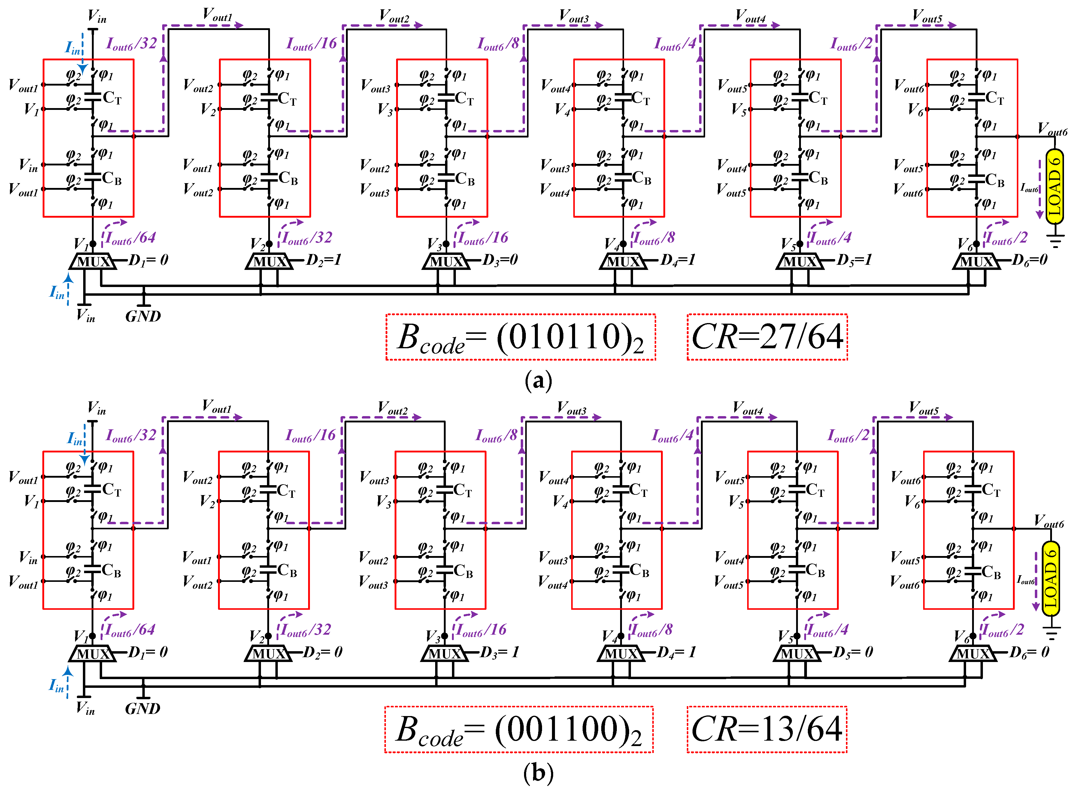
3.2.2. Multi-Output Case

Figure 8 shows the current flows of the same 6-bit SSC-DVS, as the single-output case, above using the same configuration codes. It was; however, configured to generate multi-outputs simultaneously. Figure 8a,b show the current flows in each stage for codes Bcode = (010110)2 and Bcode = (001100)2, respectively.
Equation (7) represents the current I S n of the nth stage in terms of its load current and the input current taken by its next stage, which was the (n+1)th stage. The current I i n drawn from the input voltage source Vin could be expressed by Equation (8). It was expressed by the half of the sum of the individual current for the stages that were supplied by Vin. Equation (9) describes the current I i n as a function of the output current and the conversion ratio of each stage where CRn is the conversion ratio of the n-th stage. By substituting Equation (10) in Equation (9), the Iin could be expressed by Equation (11).
I S n = I o u t n + 1 2 ( n + 1 ) × I S ( n + 1 )
I i n = 1 2 ( I S 1 ( D 1 + 1 ) + I S 2 D 2 + + I S n D n )
I i n = C R 1 I o u t 1 + C R 2 I o u t 2 + + C R n I o u t n
I o u t n = V o u t n R L n = C R n × V i n R L n
I i n = V i n × ( C R 1 2 R L 1 + C R 2 2 R L 2 + + C R n 2 R L n )
Equation (12) to Equation (17) describe the current that was provided from each stage for the example of Figure 8.
I S 1 = I o u t 1 + 1 2 I o u t 2 + 1 4 I o u t 3 + 1 8 I o u t 4 + 1 16 I o u t 5 + 1 32 I o u t 6
I S 2 = I o u t 2 + 1 2 I o u t 3 + 1 4 I o u t 4 + 1 8 I o u t 5 + 1 16 I o u t 6
I S 3 = I o u t 3 + 1 2 I o u t 4 + 1 4 I o u t 5 + 1 8 I o u t 6
I S 4 = I o u t 4 + 1 2 I o u t 5 + 1 4 I o u t 6
I S 5 = I o u t 5 + 1 2 I o u t 6
I S 6 = I o u t 6
In the 6-bit SSC-DVS example of Figure 8a, configured by Bcode= (010110)2, six output voltages were achieved simultaneously with conversion ratios of 1 2 ,   3 4 ,   3 8 ,   11 16 ,   27 32 , and 27 64 , respectively. Each SSC stage provided an output current for its own load and for the next stage as well. By substituting these conversion ratios in Equation (10) with Vin = 1.5 V and all load resistances with RL1 = RL2 = = RL6 = 2 KΩ, the estimated total input current drawn from Vin source was Iin ≈ 1.736 mA.
In the example of Figure 8b, a code Bcode= (001100)2 was applied to produce six outputs with conversion ratios of 1 2 ,   1 4 ,   5 8 ,   13 16 ,   13 32 , and 13 64 , respectively. By substituting these conversion ratios in Equation (10) with the same conditions as in the previous example, the total input current drawn by the source was calculated as Iin ≈ 1.177 mA.
Figure 10 shows a comparison between error currents that came from each stage based on the simulation and calculation in the example of Figure 8a. Both the ideal and calculated currents were estimated using Equations (12)–(17). The ideal current employed these equations with the assumption of ideal Voutn (no-load was connected), while the simulated current employed Voutn obtained from simulations with load resistances of RL1 = RL2 = = RL6 = 10 KΩ. It showed a maximum error of 2.6% between the simulated and ideal, while it showed a maximum error of 1.8% between the calculated and ideal. Figure 10 validates the correctness of the equations by proving that the equations well match the simulation results of the current per stages.
Figure 11 shows the error current of calculated and simulated input currents, which were drawn from Vin for the example of Figure 8a when the load resistance was varied from 1 to 60 KΩ. The error current curve shows that the simulated and calculated currents matched well in general, with the largest difference of less than only 7.5%, which occurred when a heavy load was connected. Figure 11 shows that Equation (11) perfectly matched the simulation results when a light load was connected.

3.3. Efficiency Analysis

This subsection analyzes the energy efficiency of the proposed SSC-DVS architecture. We used the example of 1-bit SSC-DVS in Figure 1 again for simplicity. Figure 12 represents the charge transfer model for 1-bit SSC-DVS. Here, Ceq is the equivalent capacitance of the flying capacitance CT and CB, where Ceq = CT + CB. RP is the parasitic resistance. For simplicity, we assume that RP is negligible in the remaining analysis.
If the maximum voltage VCmax across Ceq is larger than the minimum output voltage Voutmin, the charges in Ceq gets shared with CL and also gets dissipated by RL until CL is fully charged and ICL becomes 0 A, as shown in Figure 13. Right after this process, capacitors Ceq and CL transfer part of their energy to the load resistor RL. Depending on the status of CL, we analyze the energy efficiency in two phases: (1) charge distribution phase, and (2) delivery phase.

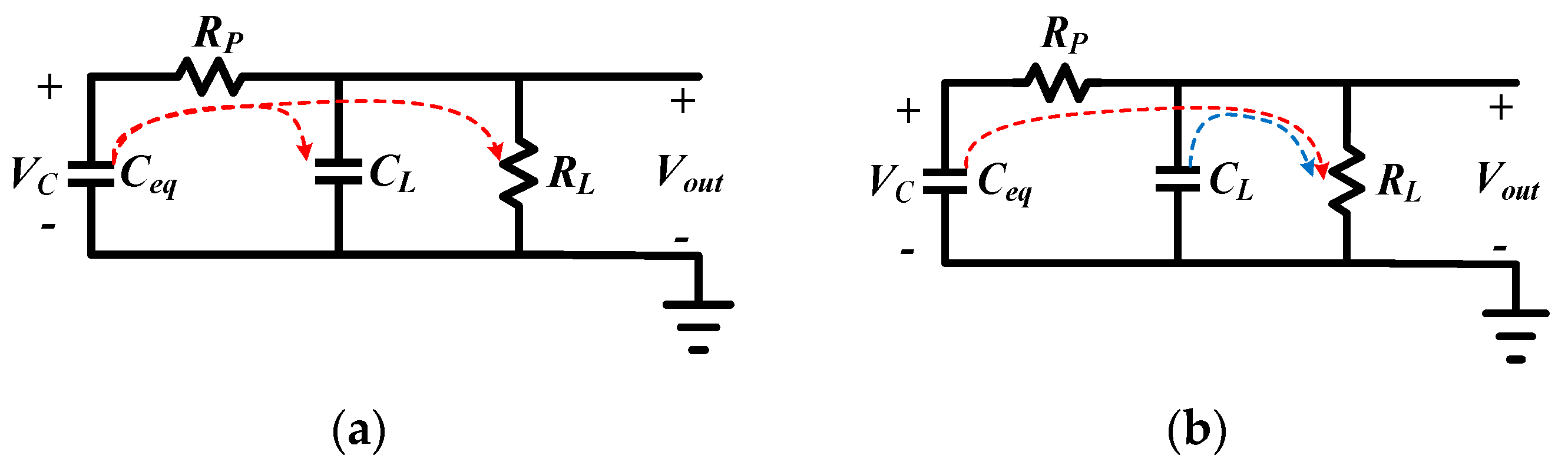
3.3.1. Charge Distribution Phase

Due to unbalanced initial voltages on Ceq and CL, when VCmax > Voutmin, Ceq delivers charges to CL and RL until CL is fully charged. By using the charge conservation principle, we can model the amount of charge delivered from Ceq to CL and RL by Equation (18). Let IRL represent the total load current drawn by the load circuit. For the sake of simplicity of proving the concept, we assume in this paper that the load current is constant regardless of the load’s supply voltage changes. Hence, we can model the load circuit by a resistor RL.
C e q ( V C m a x V C m i n ) = C L ( V o u t m a x V o u t m i n ) + I R L T C D
Here, VCmin is the voltage of Ceq after the charge distribution process, while Voutmax is the voltage of CL after the charge distribution process. In addition, TCD is the time duration for the charge distribution process to reach the condition VCmin = Voutmax. The maximum output voltage can be expressed by Equation (19). The average output current IRL can be calculated by Equation (20) under the assumption that TCD is much smaller than the time constant of the circuit.
V o u t m a x = C e q V C m a x + ( C L T C D 2 R L ) V o u t m i n C e q + C L + T C D 2 R L
I R L = V o u t m a x + V o u t m i n 2 × 1 R L

3.3.2. Delivery Phase

In the delivery phase, capacitors Ceq and CL transfer part of their charges to the load resistor RL in the remaining time of ( T 2 T C D ) , where T 2   is half of the switching period. By applying the charge conservation principle, we can model the amount of charge delivered from Ceq and CL to RL by Equation (21), while we can calculate the final voltage across the Ceq and CL by Equation (22), assuming that RP is negligible like in subsection C.
C e q ( V o u t m a x V C m i n ) + C L ( V o u t m a x V o u t m i n ) = I R L ( T 2 T C D )
V o u t m i n = V o u t m a x × ( ( C e q + C L ) R L ( T 2 T C D ) ( C e q + C L ) R L + ( T 2 T C D ) )

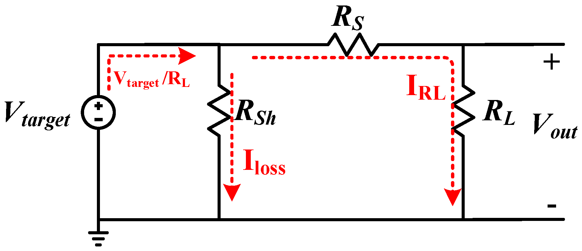
3.3.3. Losses Analysis

In SC voltage converters there are two kinds of losses that are dependent or independent of the load current IRL. The losses that are dependent on the output current include SC loss and switch conduction loss. While the losses that are independent (current loss, Iloss) of the output current include the gate and bottom plate capacitor switching losses [22,23].
Figure 14 presents a model to calculate the total power loss in the proposed circuit. In Figure 14, the independent losses were modeled by a series resistance RS, while the independent losses were modeled by a shunt resistance RSh. The total power losses in the proposed circuit can be expressed by Equation (23)
P L o s s = P R S + P R S h
P R S = ( I R L ) 2 × R S
P R S h = ( I l o s s ) 2 × R S h = ( V t a r g e t R L I R L ) 2 × R S h
The equivalent series resistance could be calculated by Equation (26), which was derived based on Equations (6) and (7) in reference [22]. While the equivalent shunt resistance could be calculated by Equation (27), which was derived based on Equations (10) and (11) in [22].
R S = 1 M C a p C e q F s w + R o n M S w W S w
R S = 1 M b o t t C b o t t F s w + 1 W S w C g a t e F s w
Here, MCap is a constant related to the converter’s output resistance and it determined based on the converter topology (e.g., for the SSC MCap = 4). Fsw is the switching frequency, Ron is the switch resistance density, which is measured in Ω·m, WSw is the total width of all transistors, and MSw is a constant which is determined by the converter’s topology (e.g., for the SSC MSw = 16). Mbott is a constant related to the converter’s topology (e.g., for the SSC Mbott = 2), Cbott is the bottom plate capacitance, and Cgate is the gate capacitance density in F/m of the switches.
Based on Equations (19) and (22) we could calculate the average output voltage; thus, we could estimate the power that delivered to the load Pout. We could, also, calculate the power loss by the proposed SSC by using Equation (20) and Equations (23)–(27). Thus, we could calculate the efficiency by Equation (28) as well.
η = P o u t P o u t + P l o s s
Table 3 shows the simulation and calculation results of the power efficiency for the 1-bit SSC-DVS example shown in Figure 1. Schematic-level circuit simulations were conducted with two different loads, of 2 and 10 KΩ. We measured the maximum voltage across Ceq for both stages from simulation, then we calculated the average output voltage using Equations (19) and (22). Table 3 validates the accuracy of Equations (19), (22), and (28) in estimating the output voltage and efficiency. Table 3 shows that the results calculated by our analytical model (Equations (19)–(28)) closely matched the simulation results. The difference in the output voltage and efficiency, respectively, was less than 1 mV and less than 0.05%.

4. Experimental Results

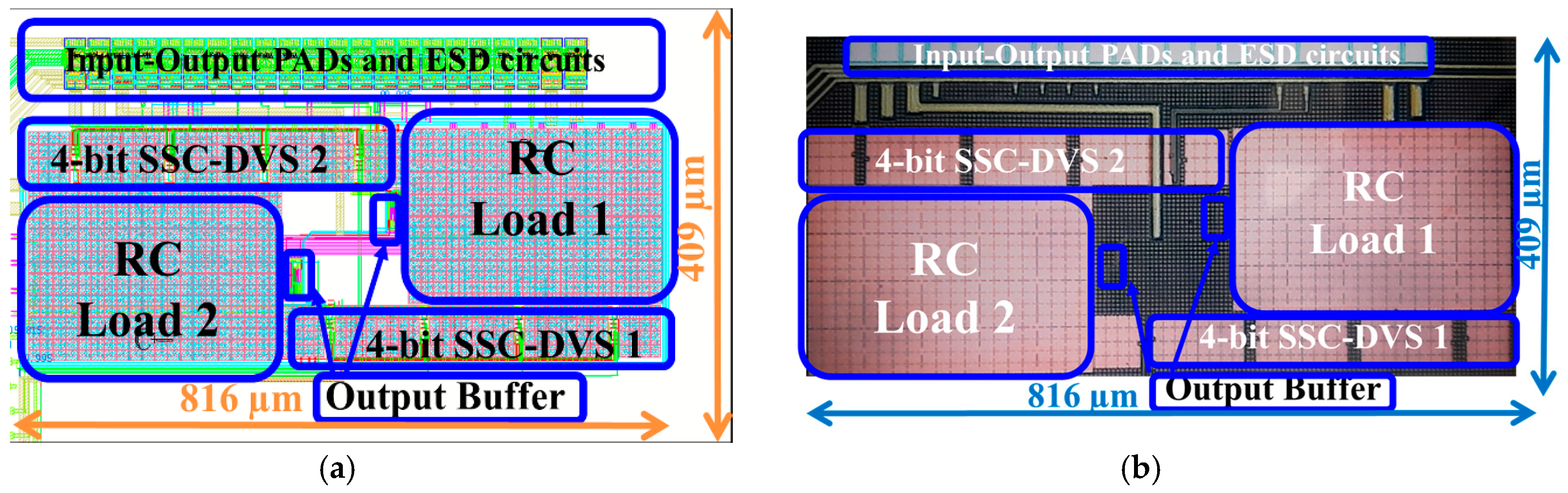
4.1. Experimental Environment

We have implemented a test chip of the proposed dynamic voltage scaler using a 130 nm CMOS process. The design, simulation, and implementation were carried out using the Spectre simulator tool of the Cadence Design Suite. Figure 15 shows the circuit schematic of the implemented 4-bit SSC-DVS that provides 16 voltage levels. We supplied Vin of the SSC-DVS with 1.5 V, while connecting the output to a simple load circuit. The load circuit was modeled by a resistor, RL, of 2 KΩ in parallel with a load capacitor, CL, of 1 nF (twice the flying capacitors) to demonstrate the performance of the proposed voltage scaler. Figure 16a shows the layout design of the test chip, while Figure 16b shows the micro-photo of its fabricated silicon. Due to area limitation in the silicon, we implemented a small 4-bit SSC-DVS architecture with on-chip capacitors of a small size of 0.4 nF, with RC load of 1 nF and 2 KΩ.

4.2. Performance of thePproposed Swapping DVS

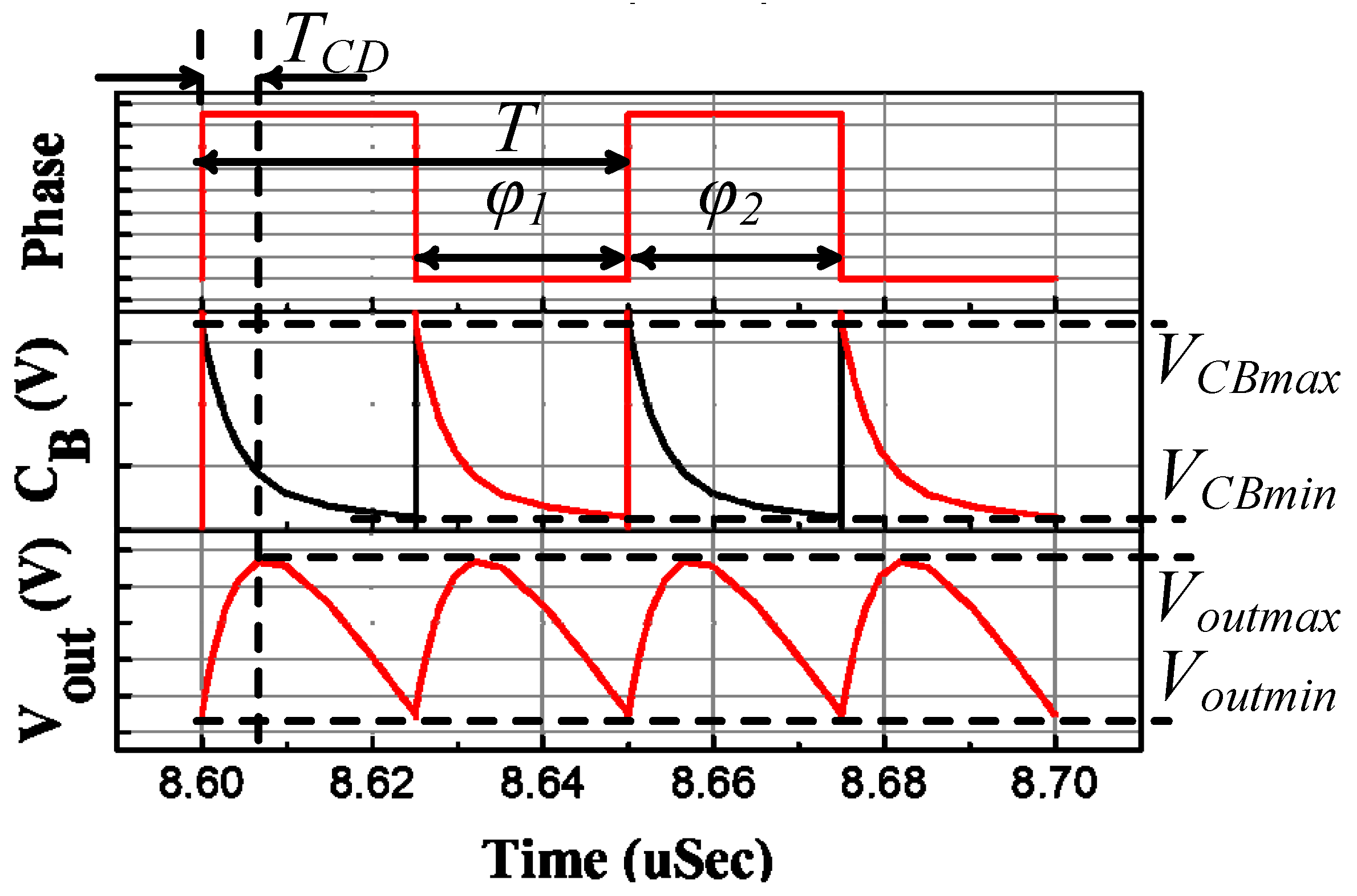
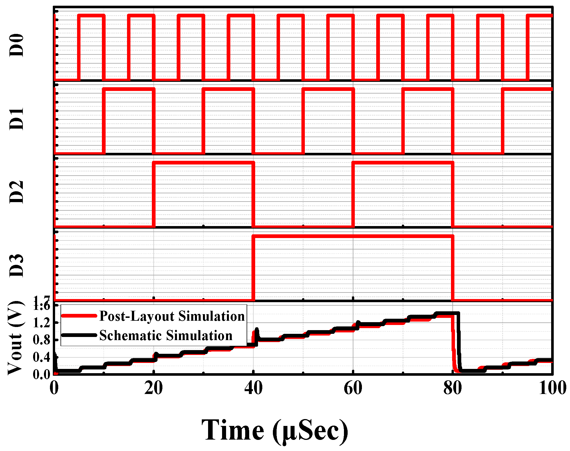
4.2.1. Target Output Voltage

Figure 17 shows the simulation result of the output voltage of the implemented 4-bit SSC-DVS. It shows accurate 16 output voltage levels based on the configuration code D1D2D3D4. It also compares the circuit simulation results with the post-layout simulation results. Figure 17 shows the two simulation results that demonstrate 16 voltage levels. The circuit simulation, highlighted by black color, produced Vout from 82.3 mV to 1.42 V with a resolution of 85 mV. On the other hand, the post-layout simulation, indicated by red color, generated Vout of 16 output voltage levels from 80.76 mV to 1.35 V with 80 mV resolution. The voltage step of the output for this example circuit could be calculated by Equation (3) as 93.75 mV. The difference in Vout’s step-size between the analysis result and the circuit schematic simulation was 11.23 mV, while the difference in Vout’s step-size between the analysis result and the post-layout simulation was 13.75 mV. These differences were attributed to the voltage drop across the switches and parasitic components.
Figure 18 illustrates the measured results of the proposed SSC-DVS. It shows accurate 16 output voltage levels from 45 mV to 1.424 V for Vout4, while it shows accurate eight output voltage levels from 117 mV to 1.242 V for Vout3.
Figure 19 shows the measured settling time of the SSC-DVS. It shows 900 nS when the target output voltage was reconfigured from 465 to 550 mV, with an input supply of 1.5 V when the load current was 275 µA. It shows, also, a very small overshooting voltage of 5 mV.
Figure 20 shows the post-layout simulation results of the load regulation when the load current changes. When the target output voltage was set to 1.031 V and the load current received a perturbation by digital control signals, we observed fluctuation of the output voltage. Figure 20 shows negative and positive transitions of the output voltage when the current changed from 50 to 495 µA and from 495 to 50 µA. The settling time for load regulation was 300 ns for the negative transition, while the settling time was 360 ns for the positive transition.

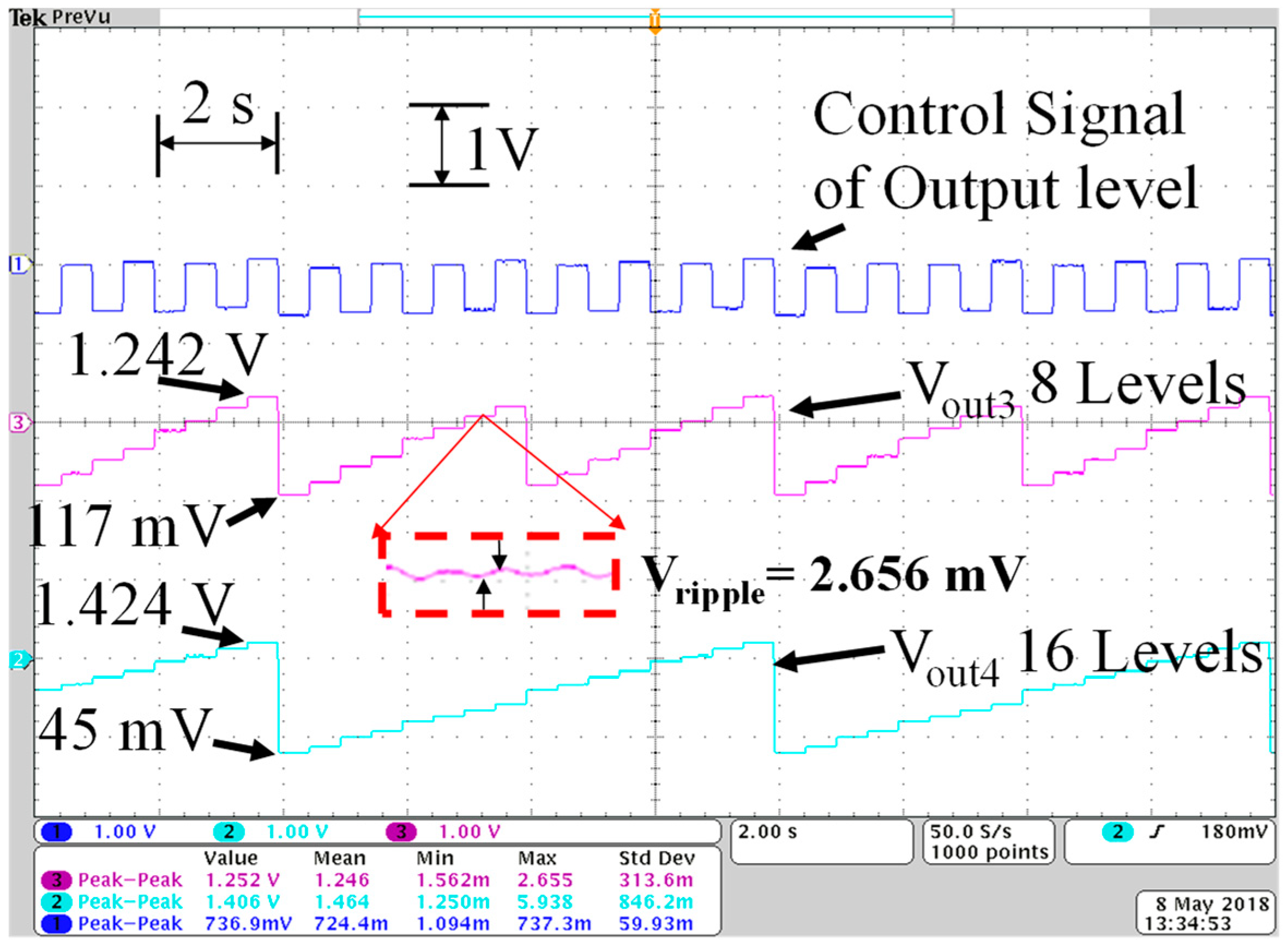
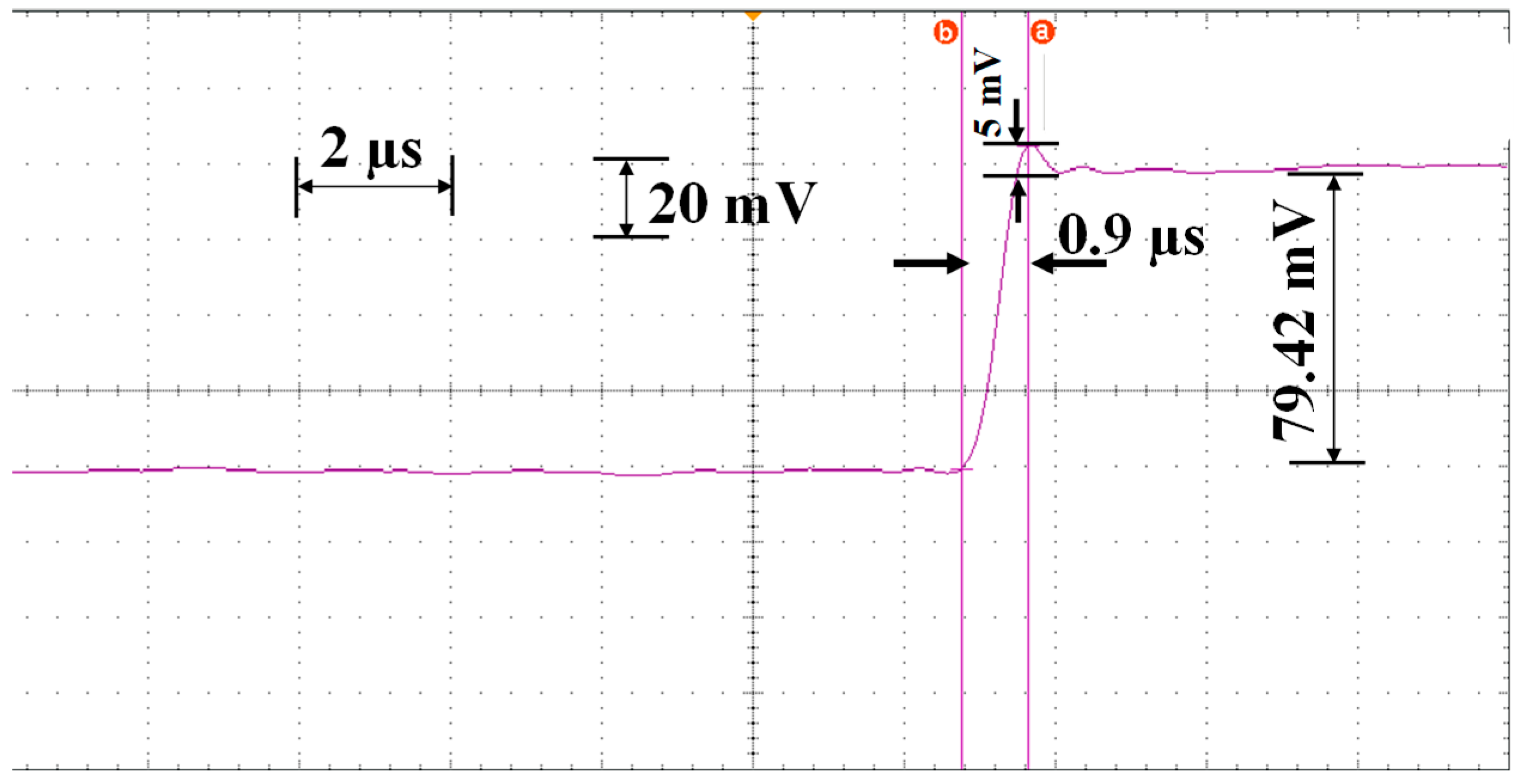
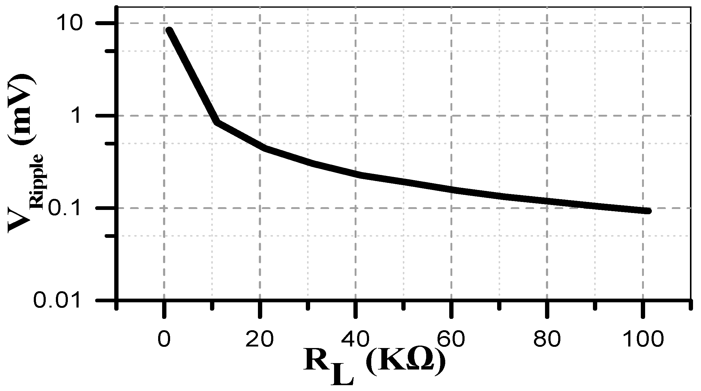
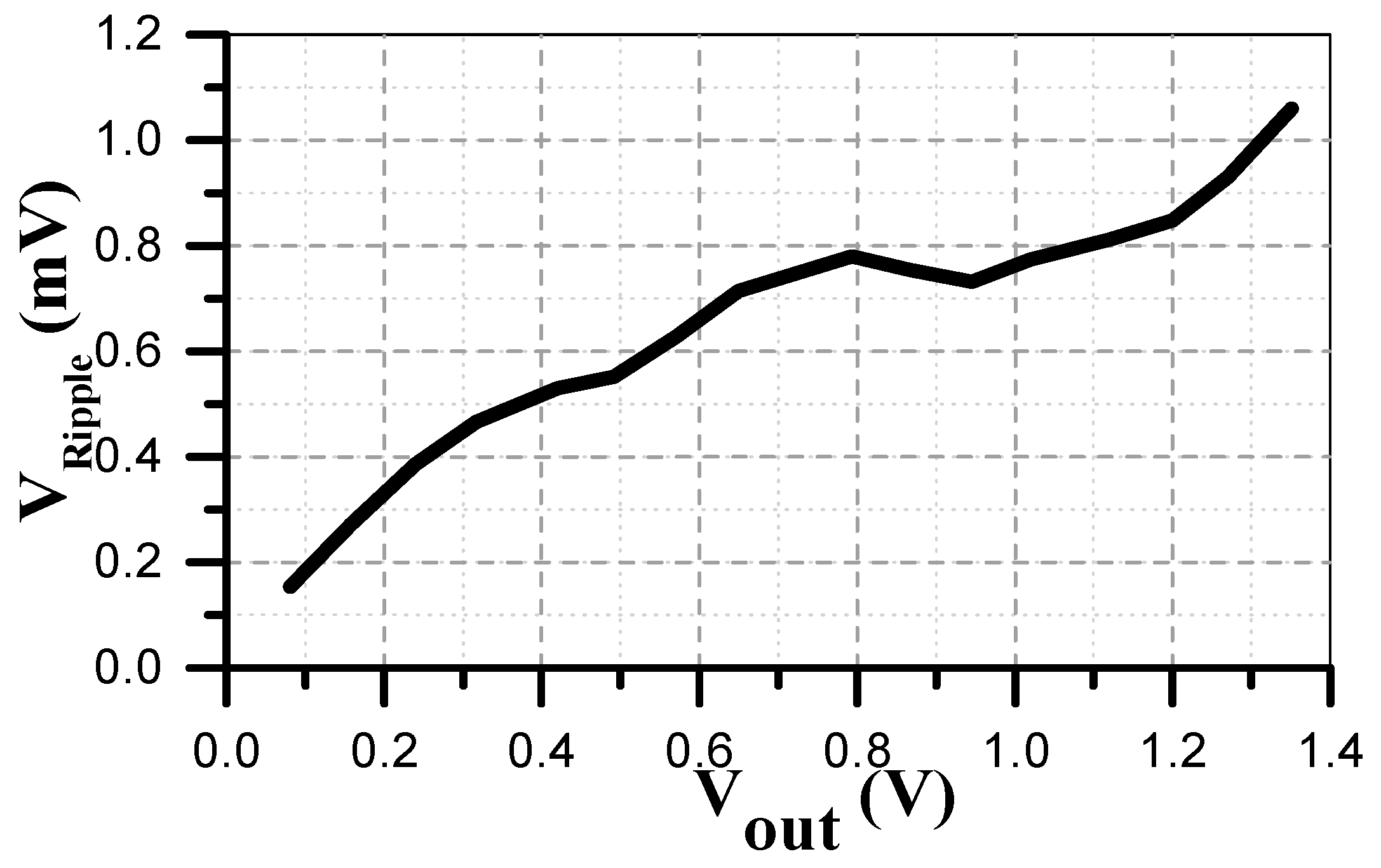
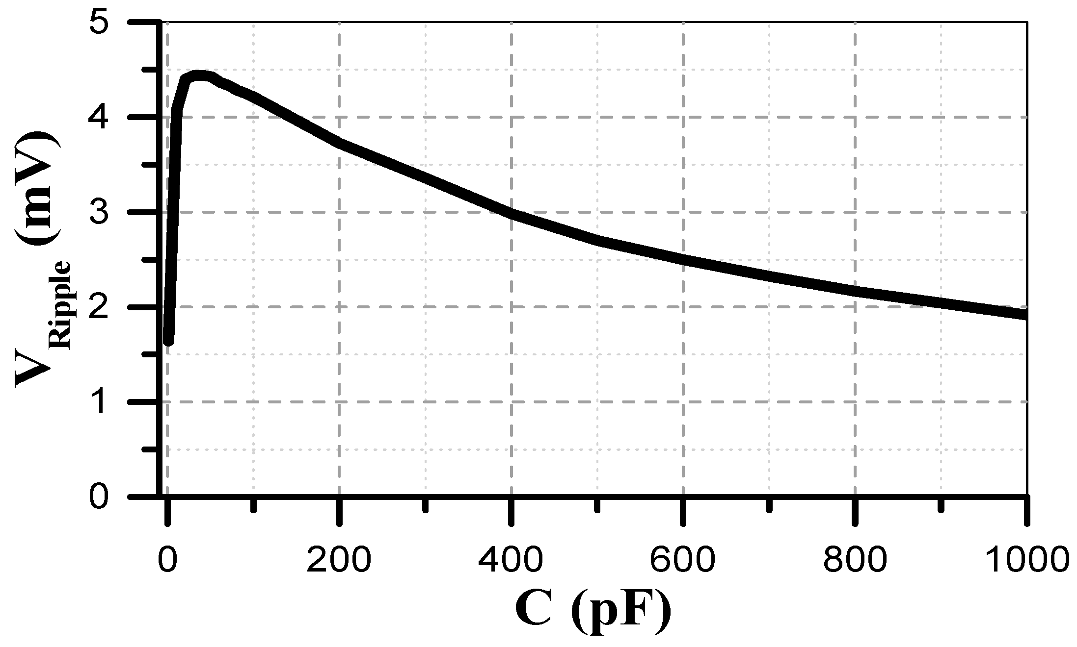
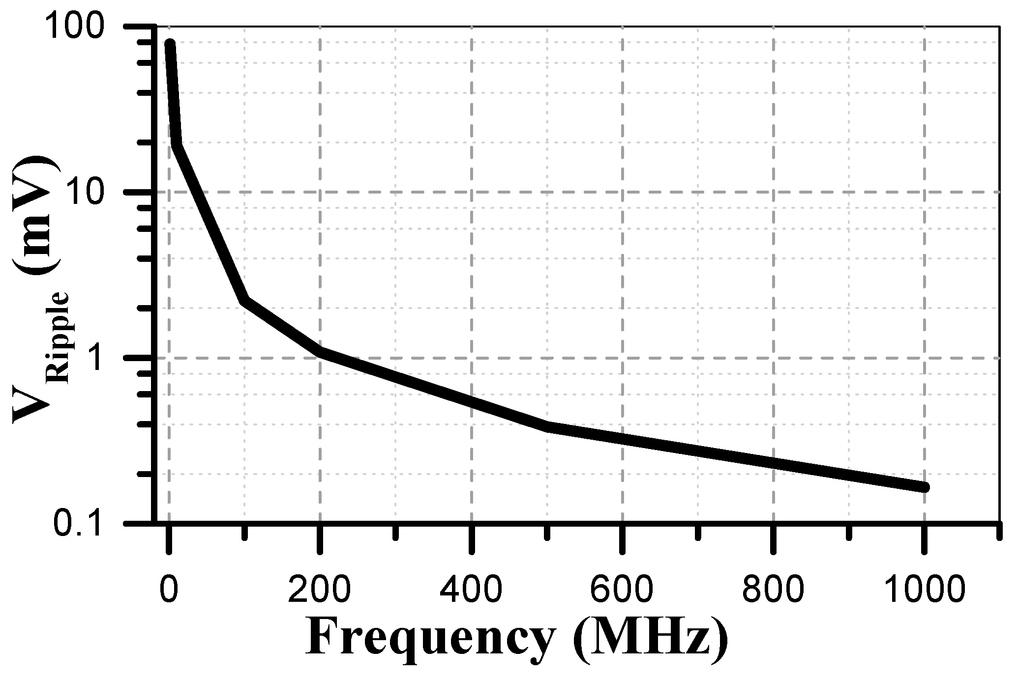
4.2.2. Voltage Ripples
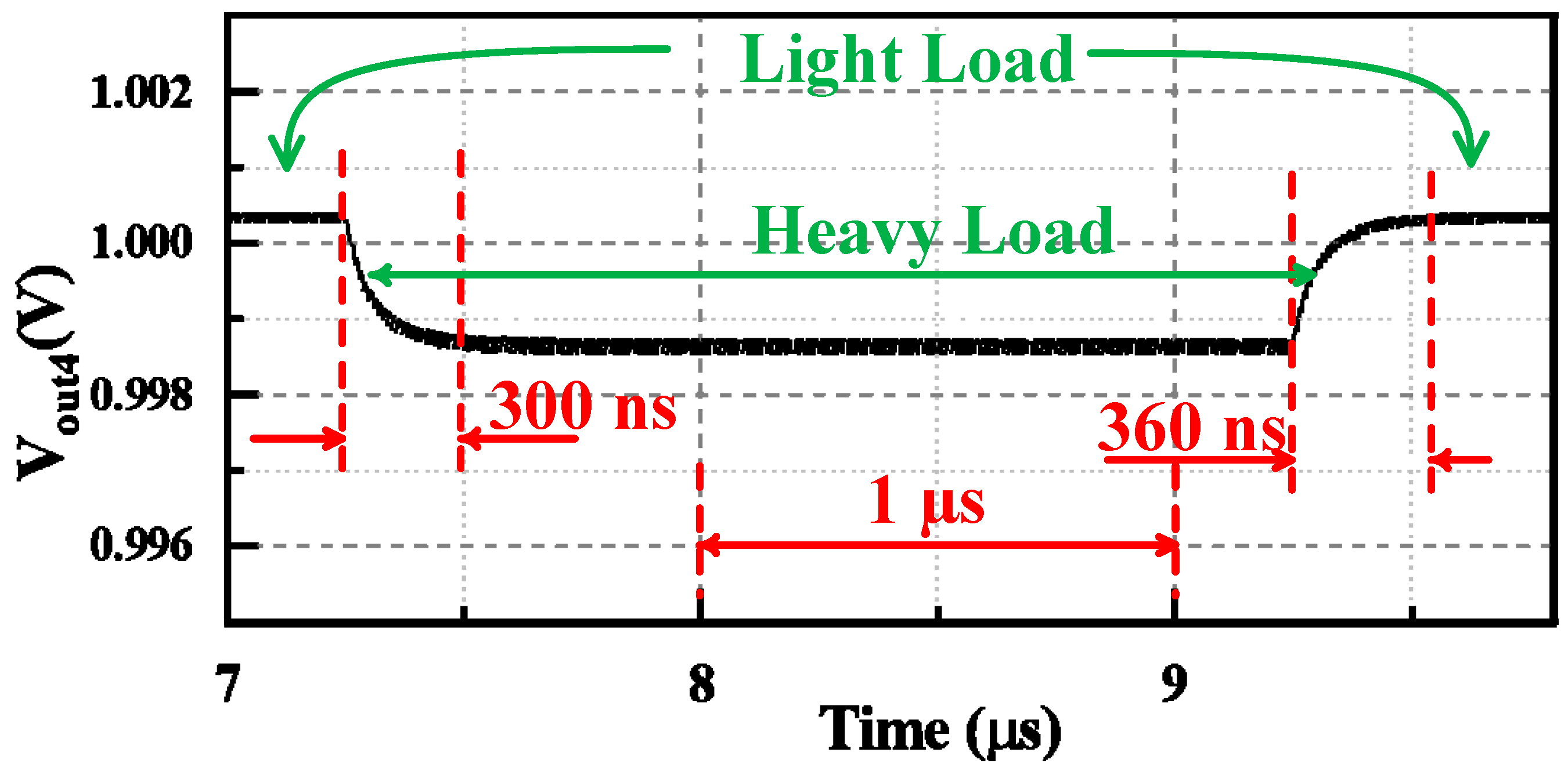
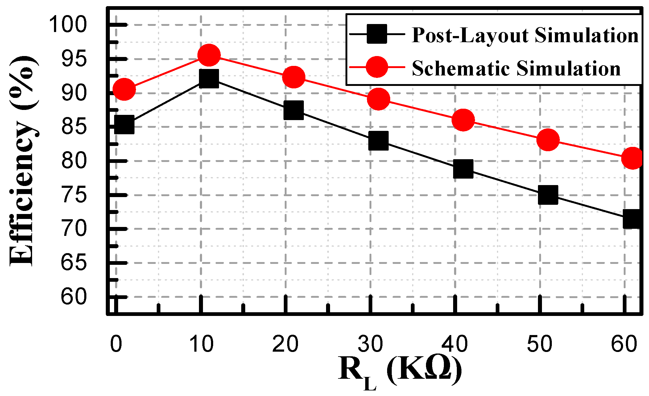
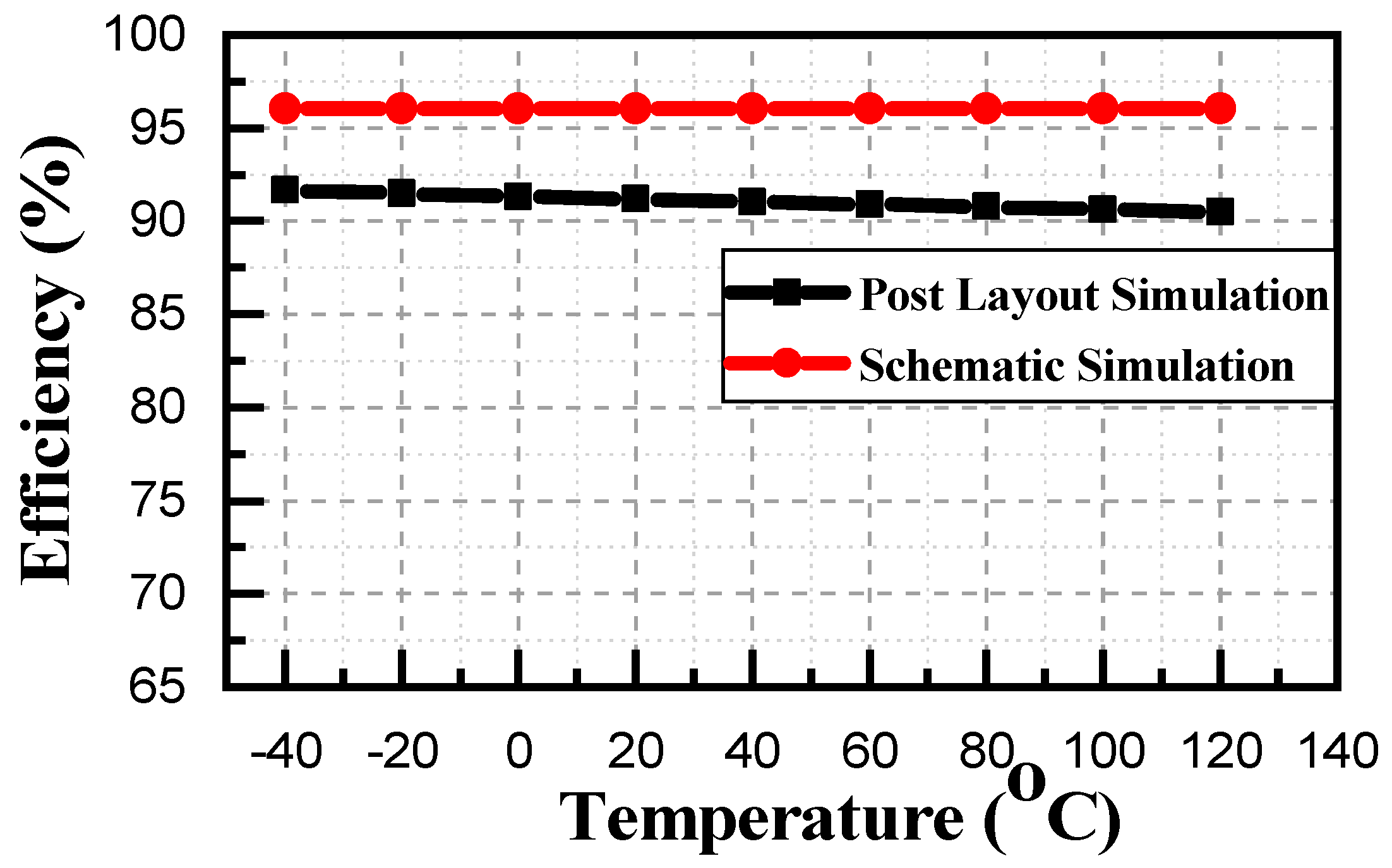
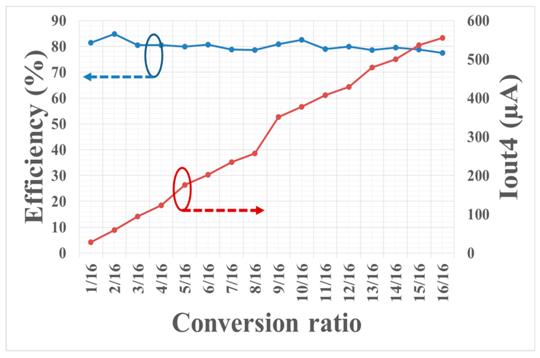
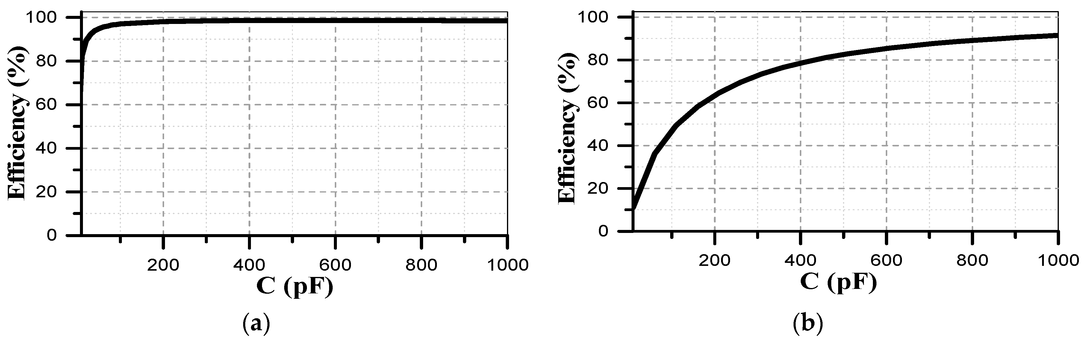
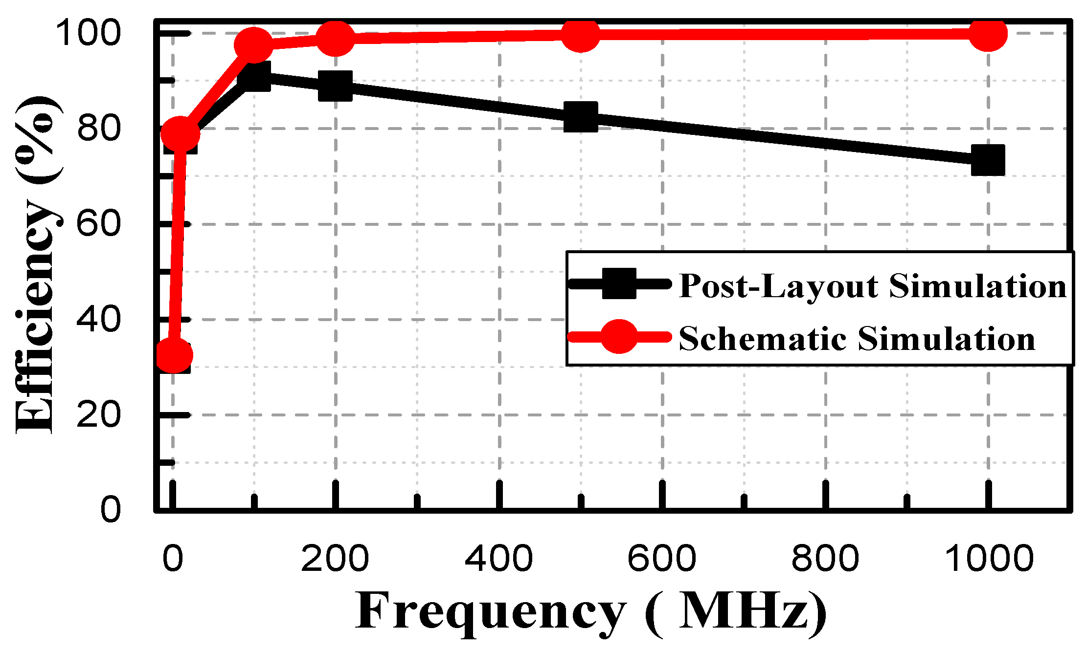
Figure 21 shows the post-layout simulation result of the output voltage ripple for the above SSC-DVS test chip, which was obtained with a wide range of capacitor size. It can be observed that the voltage ripple ranged from 1.5 to 4.5 mV. This small ripple voltage was obtained thanks to the highly-efficient recharging operation of the swapping capacitors. It also shows that the voltage ripple further decreased when the capacitor size increased.
Figure 22 shows the post-layout simulation result of the voltage ripple along with a wide range load resistance RL. It changed exponentially from 90 µV to 8.43 mV, a significantly smaller ripple voltage than previous designs reported in [9,13,15].
Figure 23 shows the post-layout simulation result of the voltage ripple along with varying switching frequency FSW. It varied exponentially from 78.3 to 0.166 mV along with a frequency range from 1 MHz to 1 GHz. The larger ripple voltage at low frequency was attributed to the fact that the difference ( Δ V = V C B V o u t ) between the voltage across the bottom capacitors CBi and the voltage across the load resistor increased as the frequency decreased. This increased voltage ripple led to a slight loss in efficiency.
Figure 24 shows the post-layout simulation result of the voltage ripple along with varying target output voltage Vout. In this simulation, we applied Vin = 1.5 V, FSW = 50 MHz, C = 50 pF, and RL = 2 KΩ. The voltage ripple changed almost linearly from 0.15 to 1.1 mV.
Figure 18 shows that the measured output voltage ripple for the SSC-DVS test chip was 2.656 mV. This small ripple voltage demonstrated that the proposed SSC-DVS was highly efficient in minimizing voltage ripple.

4.2.3. Efficiency

Figure 25 shows the efficiency of the proposed SSC-DVS obtained by post-layout simulations with varying capacitor size C. Figure 25a shows that it provided very high efficiency for most of the capacitor size, while it loss the efficiency down to 80% for the capacitor size below 1 pF. In order to maintain high efficiency in the case of small capacitors, we could use a higher switching frequency.
Figure 26 presents the simulation results of the efficiency for varying the load resistance RL. In Figure 26, the schematic simulations showed high efficiency from 90% to 95% for heavy load cases, with RL < 25 KΩ. This efficiency was measured as 85% to 92% when tested with post-layout simulations. This difference between the schematic simulation and post-layout simulation was due to the parasitic capacitance and resistance considered in the post-layout simulation.
Figure 27 illustrates the circuit simulation and the post-layout simulation of the efficiency for varying switching frequency, FSW. The circuit simulation shows the efficiency increased exponentially from 30% at FSW = 1 MHz to 99% at FSW = 1 GHz. For higher FSW values, the efficiency saturated at 99%. In other words, the difference between the output voltage and the voltage across the bottom capacitor CB was very small. In contrast, at a very low switching frequency below 1 MHz, it exhibited a poor efficiency of 30%. This was due to slow charging and discharging operations for the bottom capacitor CB. We could keep the efficiency high by increasing the capacitor size, as shown in Figure 25b. On the other hand, in Figure 27, the post-layout simulation exhibited efficiency 10%–20% lower than the circuit simulation result for the frequency higher than 200 MHz. The lower efficiency could be explained by the fact that we used regular transistors, not radio frequency (RF) transistors for the test chip design, thus the post-layout simulation experienced higher parasitic values at high frequency.
Figure 28 presents the efficiency of the proposed architecture when the temperature varied from −40 to 120 °C. It showed almost constant efficiency of 94% for the schematic simulation, while it showed 91% efficiency for the post-layout simulation. Therefore, the proposed SSC-DVS was well suited for applications operating under large temperature changes.
Figure 29 shows the measured efficiency of the proposed SSC-DVS versus the conversion ratio and output load current of the fourth stage (Iout4). The efficiency of more than 80% was obtained with an output load current of the fourth stage (Iout4) in the range of 50–550 µA. The efficiency values lower than the simulation results were primarily attributed to the slow transition of control signals as well as the parasitic circuit elements. We expect that the efficiency of the test chip could be improved to the level of post-layout simulations if we improved the control signals by adding buffer circuits.

4.3. Comparison

Table 4 compares the key properties of the proposed SSC-DVS test chip with other switched-capacitor voltage converters recently published. The proposed 4-bit SSC-DVS showed 24 = 16 conversion ratios. The 4-bit recursive voltage converter of [14] shows 24 − 1 = 15 conversion ratios, while the 7-bit SAR of [9] can provide 117 conversion ratios. The designs reported in [15,16,17] show only one to three fixed conversion ratios.
The proposed SSC-DVS showed an almost rail–rail output voltage range, and; thus, it could provide extremely low supply voltages to ultra-low power applications. The design of [9] provides a limited range of supply voltages that are larger than 0.45 V, while the designs reported in [15,16,17] provide an output voltage of only 0.5 Vin or higher. Furthermore, the proposed SSC-DVS showed a smaller voltage ripple of 2.656 mV. For example, it showed around a 84% and 94% smaller voltage ripple than the recent voltage converters of [9,15], respectively. The measured results of the proposed SSC-DVS showed a peak efficiency of 85%, which was higher than the previous circuits reported in [9,16,17].
The total size of its on-chip capacitors was 400 pF, while the total area of the SSC-DVS test chip was 0.334 mm2, including the on-chip flying capacitors and output RC load.

5. Conclusions

In this paper, a reference-free, scalable, and high efficiency, multi-output DVS architecture based on n-bit swapping switched-capacitor topology is proposed. It employs n-cascaded 2:1 swapping capacitor stages to generate 2n conversion ratios with a resolution of V i n 2 n . Its swapping switched-capacitor unit forms a structure of self-biasing, and; thus, ensures that the output voltage of each stage converges to the target voltage, which is determined by the digital code configuration. Thus, SSC-DVS does not require a power-hungry reference voltage generator and comparator feedback circuits, thus it can provide significantly higher energy efficiency than previous voltage converters. A 4-bit SSC-DVS was implemented into a test chip using a 130 nm MagnaChip CMOS process. Post-layout simulations were conducted with an input voltage of 1.5 V, switching frequency of 50 MHz, and a load circuit that modeled by a load resistor of 2 KΩ. The measurements and the realistic simulations, with all layout parasitic components, demonstrated that it achieved a stable 16 output voltage levels with a step size of 80 mV, and a ripple voltage as small as 2.656 mV. SSC-DVS exhibited a peak efficiency of 85% when it supplied a load current of 550 µA—a substantially higher energy efficiency compared with previous switch-capacitor converters.

Author Contributions

A.N.R. proposed, designed, and implemented the overall architecture of the proposed SSC-DVS. He, also, measured the performance of the proposed architecture to verify the test chip. H.W.K. guided and directed the first author for this work.

Funding

This research was supported by the Center for Integrated Smart Sensors funded by the Ministry of Science, ICT, and Future Planning as Global Frontier Project (CISS-2018), and it was also supported by the Institute for Information and Communications Technology Promotion (IITP) grant, funded by the Korea Government (MSIT) with grant number (R7117-16-0164). It was also supported by SoC platform and SW development Advanced Education for IOT which is funded by the Ministry of Trade, Industry, and Energy (N00011132).

Conflicts of Interest

The authors declare no conflict of interest.

References

  1. Bang, S.Y.; Lee, Y.Y.; Kim, Y.J.; Blaauw, D.; Sylvester, D. A Fully Integrated Switched-Capacitor Based PMU with Adaptive Energy Harvesting Technique for Ultra-Low Power Sensing Applications. In Proceedings of the 2013 IEEE International Symposium on Circuits and Systems (ISCAS2013), Beijing, China, 19–23 May 2013. [Google Scholar]
  2. Kilani, D.; Alhawari, M.; Mohammad, B.; Saleh, H.; Ismail, M. An Efficient Switched-Capacitor DC-DC Buck Converter for Self-Powered Wearable Electronics. IEEE Trans. Circuits Syst. 2016, 63, 1557–1566. [Google Scholar] [CrossRef]
  3. Hasib, O.A.; Sawan, M.; Savaria, Y. A Low-Power Asynchronous Step-Down DC-DC Converter for Implantable Devices. IEEE Trans. Circuits Syst. 2011, 5, 292–301. [Google Scholar] [CrossRef]
  4. Jung, W.Y.; Oh, S.C.; Bang, S.Y.; Lee, Y.Y.; Foo, Z.; Kim, G.H.; Zhang, Y.; Sylvester, D.; Blaauw, D. An Ultra-Low Power Fully Integrated Energy Harvester Based on Self-Oscillating Switched-Capacitor Voltage Doubler. IEEE J. Solid-State Circuits 2014, 49, 2800–2811. [Google Scholar] [CrossRef]
  5. Lueders, M.; Evermann, B.; Gerber, J.; Huber, K.; Kuhn, R.; Zwerg, M.; Schmitt-Landsiedel, D.; Brederlow, R. Architectural and Circuit Design Techniques for Power Management of Ultra-Low-Power MCU Systems. IEEE Trans. Very Large Scale Integr. (VLSI) Syst. 2014, 22, 2287–2296. [Google Scholar] [CrossRef]
  6. Ragheb, A.; Kim, H. Ultra-low power OTA based on bias recycling and subthreshold operation with phase margin enhancement. Microelectron. J. 2017, 60, 94–101. [Google Scholar] [CrossRef]
  7. Huang, C.; Mok, P.K.T. A 100 Mhz 82.4% efficiency package bondwire based four-phase fully-integrated buck converter with flying capacitor for area reduction. IEEE J. Solid-State Circuits 2013, 48, 2977–2988. [Google Scholar] [CrossRef]
  8. Xiao, J.; Peterchev, A.; Zhang, J.; Sanders, S. An ultra-low-power digitally controlled buck converterIC for cellular phone applications. In Proceedings of the Nineteenth Annual IEEE Applied Power Electronics Conference and Exposition (APEC’04), Anaheim, CA, USA, 22–26 February 2004; pp. 383–391. [Google Scholar]
  9. Bang, S.Y.; Blaauw, D.; Sylvester, D. A Successive-Approximation Switched-Capacitor DC-DC Converter with Resolution of VIN/2N for a Wide Range of Input and Output Voltages. IEEE J. Solid-State Circuits 2016, 51, 543–556. [Google Scholar]
  10. Kim, W.Y.; Brooks, D.; Wei, G.-Y. A Fully-Integrated 3-Level DC-DC Converter for Nanosecond-Scale DVFS. IEEE J. Solid-State Circuits 2012, 47, 206–219. [Google Scholar] [CrossRef]
  11. Hua, Z.; Lee, H. A Reconfigurable Dual-Output Switched-Capacitor DC-DC Regulator with Sub-Harmonic Adaptive-On-Time Control for Low-Power Applications. IEEE J. Solid-State Circuits 2015, 50, 724–736. [Google Scholar] [CrossRef]
  12. Sanders, S.R.; Alon, E.; Le, H.P.; Seeman, M.D.; John, M.; Ng, V.W. The road to fully integrated DC–DC conversion via the switched-capacitor approach. IEEE Trans. Power Electron. 2013, 28, 4146–4155. [Google Scholar] [CrossRef]
  13. Ragheb, A.N.; Kim, H.; Lee, J.-J. 84% High efficiency dynamic voltage scaler with nano-second settling time based on charge-pump and BWC-DAC. Microelectron. J. 2018, 79, 91–97. [Google Scholar] [CrossRef]
  14. Salem, L.G.; Mercier, P.P. A Recursive Switched-Capacitor DC-DC Converter Achieving 2N-1 Ratios with High Efficiency over a Wide Output Voltage Range. IEEE J. Solid-State Circuits 2014, 49, 2773–2787. [Google Scholar] [CrossRef]
  15. Turnquist, M.; Hiienkari, M.; Mäkipää, J.; Koskinen, L. A fully integrated 2:1 self-oscillating switched-capacitor DC-DC converter in 28 nm UTBB FD-SOI. J. Low Power Electron. Appl. 2016, 6, 17. [Google Scholar] [CrossRef]
  16. Nielsen-Lónn, M.; Angelov, P.; Wikner, J.J.; Alvandpour, A. Self-oscillating multilevel switched-capacitor DC/DC converter for energy harvesting. In Proceedings of the 2017 IEEE Nordic Circuits and Systems Conference (NORCAS): NORCHIP and International Symposium of System-on-Chip (SoC), Linkoping, Sweden, 23–25 October 2017; pp. 1–5. [Google Scholar]
  17. Butzen, N.; Steyaert, M.S.J. Design of Soft-Charging Switched-Capacitor DC–DC Converters Using Stage Outphasing and Multiphase Soft-Charging. IEEE J. Solid-State Circuits 2017, 52, 3132–3141. [Google Scholar] [CrossRef]
  18. Rodríguez-Pérez, A.; Delgado-Restituto, M.; Medeiro, F. Impact of parasitics on even symmetric split-capacitor arrays. Int. J. Circuit Theor. Appl. 2013, 41, 972–987. [Google Scholar] [CrossRef]
  19. Chiu, P.-Y.; Ker, M.-D. Metal-layer Capacitors in the 65nm CMOS Process and the Application for Low-Leakage Power-Rail ESD Clamp Circuit. Microelectron. Reliab. 2013, 54, 64–70. [Google Scholar] [CrossRef]
  20. Ju, Y.M.; Shin, S.-U.; Huh, Y.; Park, S.-H.; Bang, J.-S.; Kim, K.-D.; Choi, S.-W.; Lee, J.-H.; Cho, G.-H. 10.4 A hybrid inductor-based flying-capacitor-assisted step-up/step-down DC-DC converter with 96.56% efficiency. In Proceedings of the 2017 IEEE International Solid-State Circuits Conference (ISSCC), San Francisco, CA, USA, 5–9 February 2017; pp. 184–185. [Google Scholar]
  21. Favrat, P.; Deval, P.; Declercq, M.J. A high-efficiency CMOS voltage doubler. IEEE J. Solid-State Circuits 1998, 33, 410–416. [Google Scholar] [CrossRef]
  22. Le, H.; Sanders, S.R.; Alon, E. Design Techniques for Fully Integrated Switched-Capacitor DC-DC Converters. IEEE J. Solid-State Circuits 2011, 46, 2120–2131. [Google Scholar] [CrossRef]
  23. Seeman, M. A Design Methodology for Switched-Capacitor DC-DC Converters. Ph.D. Dissertation, University of California, Berkeley, CA, USA, May 2009. [Google Scholar]
Figure 1. The basic unit cell of the proposed SSC (Swapping Switched-capacitor): (a) Schematic of the unit cell; (b) phase 1; and (c) phase 2.
Energies 12 00625 g001
Figure 2. Block diagram of the proposed n-bit SSC-DVS (Dynamic Voltage Scaler) architecture.
Energies 12 00625 g002
Figure 3. The schematic diagram for the proposed n-bit SSC-DVS architecture.
Energies 12 00625 g003
Figure 4. Transmission-gate switch with body switch that was used in the proposed SSC-DVS.
Energies 12 00625 g004
Figure 5. A 2-bit example of the proposed SSC-DVS architecture with two configurations of: (a) D1D2 = (00)2; and (b) D1D2 = (01)2.
Energies 12 00625 g005
Figure 6. A small example of 2-bit SSC-DVS architecture with conversion ratios of 1 2 and 1 4 : (a) Phase 1 (φ1); and (b) phase 2 (φ2).
Energies 12 00625 g006
Figure 7. A small example of 2-bit SSC-DVS architecture with conversion ratios of 1 2 and 3 4 : (a) Phase 1 (φ1); and (b) phase 2 (φ2).
Energies 12 00625 g007
Figure 8. A 6-bit SSC-DVS with multi-outputs based on: (a) Bcode= (010110)2; and (b) Bcode= (001100)2.
Energies 12 00625 g008
Figure 9. A 6-bit SSC-DVS with single-output based on: (a) Bcode= (010110)2; and (b) Bcode= (001100)2.
Energies 12 00625 g009
Figure 10. Comparison between simulated and calculated input currents errors per stage.
Energies 12 00625 g010
Figure 11. Input current error drawn by the source Vin with varying RL load.
Energies 12 00625 g011
Figure 12. Charge transfer model of 1-bit SSC: (a) Charge distribution phase; and (b) delivery phase.
Energies 12 00625 g012
Figure 13. Voltage waveforms of phase control signal, CB, and output load Vout.
Energies 12 00625 g013
Figure 14. Simplified model for power loss calculations.
Energies 12 00625 g014
Figure 15. Schematic of the implemented 4-bit SSC-DVS.
Energies 12 00625 g015
Figure 16. (a) Layout and (b) die micro-photograph of the proposed SSC-DVS architecture.
Energies 12 00625 g016
Figure 17. The simulation and post-simulation results of the output voltage levels of the proposed SSC-DVS.
Energies 12 00625 g017
Figure 18. The measured results of the output voltage levels and the ripple voltage of the proposed SSC-DVS.
Energies 12 00625 g018
Figure 19. The measured results of settling time of the proposed SSC-DVS architecture.
Energies 12 00625 g019
Figure 20. The post-layout simulation results of the load transient performance of the proposed SSC-DVS architecture.
Energies 12 00625 g020
Figure 21. The post-layout simulation results of the output voltage ripple of the proposed SSC-DVS versus the flying capacitor C when Vin = 1.5 V, RL = 2 KΩ, and FSW = 50 MHz.
Energies 12 00625 g021
Figure 22. The post-layout simulation results of the output voltage ripple of the proposed SSC-DVS versus the load resistance RL when Vin =1.5 V, FSW =50 MHz, and C= 50 pF.
Energies 12 00625 g022
Figure 23. The post-layout simulation results of the output voltage ripple of the proposed SSC-DVS versus the switching frequency FSW when Vin = 1.5 V, RL = 2 KΩ, and C = 50 pF.
Energies 12 00625 g023
Figure 24. The post-layout simulation results of the output voltage ripple of the proposed SSC-DVS versus output voltage when Vin =1.5 V, RL = 2 KΩ, FSW =50 MHz, and C = 50 pF.
Energies 12 00625 g024
Figure 25. The post-layout simulation of the efficiency of the proposed SSC-DVS architecture versus flaying capacitor C when Vin =1.5 V, RL = 2 KΩ: (a) FSW = 50 MHz; and (b) FSW = 1 MHz.
Energies 12 00625 g025
Figure 26. The post-layout simulation of the efficiency of the proposed SSC-DVS architecture versus the load resistor RL when Vin =1.5 V, FSW = 50 MHz, C = 50 pF.
Energies 12 00625 g026
Figure 27. The post-layout simulation of the efficiency of the proposed SSC-DVS architecture versus the switching Frequency FSW when Vin =1.5 V, C = 50 pF, RL= 2 KΩ.
Energies 12 00625 g027
Figure 28. The simulation and post-layout simulation of the efficiency of the proposed SSC-DVS architecture versus the temperature when Vin =1.5 V, FSW = 50 MHz, C = 50 pF, RL = 2 KΩ.
Energies 12 00625 g028
Figure 29. The measured results of the efficiency versus the conversion ratio and the output load current.
Energies 12 00625 g029
Table 1. Output capacitor size versus output voltage ripple for 4-bit SSC-DVS architecture.
CL (nF)VRipple1 (mV)VRipple2 (mV)VRipple3 (mV)VRipple4 (mV)
0.52.161.721.671.72
11.10.8540.8490.955
1.50.740.5680.5670.575
20.5560.4240.4250.43
2.50.440.3350.3380.337
30.3630.280.2830.288
3.50.3170.2370.2420.245
40.2750.210.1990.212
Table 2. Two different configuration codes with conversion ratios and generated output voltages.
Bcode = (010110)2Bcode = (001100)2
VoutkCRValue (V)VoutkCRValue (V)
Vout1 1 2 0.75Vout1 1 2 0.75
Vout2 3 4 1.125Vout2 1 4 0.375
Vout3 3 8 0.5625Vout3 5 8 0.9375
Vout4 11 16 1.03125Vout4 13 16 1.2187
Vout5 27 32 1.26562Vout5 13 32 0.609
Vout6 27 64 0.6328Vout6 13 64 0.304
Table 3. Comparison of power efficiency based on simulation and calculation for 1-bit example.
ParameterRL = 10 KΩ, CR = 1 2 RL = 2 KΩ, CR = 1 2
SimulatedCalculatedSimulatedCalculated
Vout (mV)745.66745.7728.881728.95
Iout (µA)74.56674.57364.4405364.475
Iloss (µA)0.4340.4310.559510.525
Pout (µW)55.600955.6068265.6337265.684
Ploss (µW)0.6490.64615.61615.565
η (%)98.898.8594.44794.465
Table 4. Comparison between the proposed SSC-DVS converter and the previous voltage converters.
[9][14][15][16][17]This Work
Year201620142016201720172018
Tech. (nm)1802502818028130
Topology7-bit SAR4-bit recursiveSelf-oscillationMulti-level self-oscillationSoft-charging4-bit swapping
Vin (V)3.4–4.32.51–1.20.7–203.21.5
Fsw (MHz)0.08–2.70.2–10--160050
Conversion Ratio117152:1 1 2 , 1 3 , 1 4 3:116
Step Size (mV)31.25 @ Vin = 4V156---85
Vout (V)>0.450.1–2.180.38–0.4850.7–5.50.950.085–1.424
Vripple (mV)≥17.15-≤48.5--2.656
Iout (µA)30020000.172–43510.7 40.5–550
C (nF)2.530.1350.7221.50.4
Efficiency (%)728587 @ Vout = 0.4668.7 @ Vin = 7.582.685
Area (mm2)1.694.6450.1040.550.1170.334

