Abstract
The device characteristics of polymer solar cells can be improved through an annealing process. This is especially true of the carrier mobility and the light absorption of P3HT:PCBM, which improves considerably after the annealing process. In the standard structure using indium-tin-oxide (ITO) as an anode, most studies have focused on the post-annealing process, where thermal annealing is performed after device fabrication. This work reports the effects of different annealing methods for inverted polymer solar cells, using ITO as a cathode. Similar levels of light absorption and P3HT crystallinity were obtained regardless of the annealing procedure in the inverted structure. However, compared with the post-annealed device, the pre-annealed device, which was thermally annealed after deposition of the P3HT:PCBM film, exhibited better charge extraction, owing to the superior device resistances and larger MoO3 grain size. Therefore, the pre-annealing method yields better performance than the post-annealing method.
1. Introduction
Organic solar cells as a renewable energy source have many outstanding attributes, such as mechanical flexibility, light-weight, and low manufacturing cost [,]. Organic materials have a narrow absorption spectrum, short diffusion length, and low carrier mobility compared with inorganic materials. However, the efficiency of organic solar cells has been improved (by up to 17.3% from organic tandem structure []) through the synthesis of new donor/acceptor materials [,,,] and developing suitable device structures for polymer solar cells [,]. Now, organic solar cells are more efficient than Si-based thin film solar cells, allowing them to enter new markets such as BIPV (Building Integrated Photovoltaic) flexible and wearable applications [].
Recently, for improved device performance, several studies have focused on annealing processes in bulk heterojunction organic solar cells. According to these studies, the annealing process can improve the device performance by increasing the light absorption and improving the charge carrier mobility, especially in polymer solar cells based on poly (3-hexylthiopene) (P3HT):phenyl-C61-butyric acid methyl ester (PCBM) [,,,]. However, most studies on the annealing method have focused on the annealing condition for the post-annealing process in the conventional structure. The conventional structure of organic solar cells is susceptible to the corrosion of ITO, owing to the acidity of Poly (3,4-ethylenedioxythiophene): poly (styrenesulfonate) (PEDOT:PSS) and the easy oxidation of low work function metals. Therefore, an inverted structure with the transition metal oxide as a hole buffer layer has been suggested for organic solar cells. This structure, where the electrode polarities are switched, can improve the air stability through the use of an air-stable metal with high work function (e.g., Al, Ag, and Au, rather than Cs, Li, and Ca) [,,]. Furthermore, the inverted structure can be sequentially evaporated by the transition metal oxide/the anode metal without breaking the vacuum during the fabrication of the device. MoO3, a transition metal oxide, has been widely used in place of PEDOT:PSS, which suffers from charge extraction issues and acidity issues in polymer solar cells [,,,].
In this paper, we report inverted P3HT:PCBM polymer solar cells for different annealing conditions, such as non-treatment and annealing before (pre-annealing) and after the evaporation of MoO3/Al (post-annealing). We show that the performance of the pre-annealed device in the inverted structure is superior to that of the post-annealed device. Similarly, we investigate the interfacial and bulk electrical properties via electrical impedance spectroscopy and the surface morphology properties through atomic force microscopy (AFM).
2. Experimental Methods
All of the devices were prepared on indium-tin-oxide (ITO) coated glass (thickness: ~150 nm, sheet resistance: 10 Ω/□). The ITO-coated substrates were cleaned using isopropyl alcohol, de-ionized water, acetone, and methanol in an ultrasonic bath and dried in a vacuum oven. Zinc oxide (ZnO) nanoparticles (NPs) as an electron extraction layer dissolved in butanol were spin-coated on ITO substrates and then dried at 150 °C for 20 min (thickness of ZnO film: 30 nm). The ZnO NPs were prepared in accordance with []. Subsequently, the solution of P3HT (Rieke metals, 4002-E):PCBM (Nano-C) (1:0.8 by weight.) was spin-coated on the ZnO layer, thereby yielding a P3HT:PCBM film (thickness: 150 nm). After spin-coating the active layer, MoO3 as the hole extraction layer (thickness: 10 nm) and Al as the anode (thickness: 100 nm) were thermal-evaporated sequentially under a vacuum of ~10-6 Torr. The active area of the device was 0.2 cm2 (see Figure 1 for the device structure). Absorption spectra and X-ray diffraction (XRD) patterns were obtained for the P3HT:PCBM solution spin-coated on the quartz substrates and MoO3 thermal-evaporated on the P3HT:PCBM.
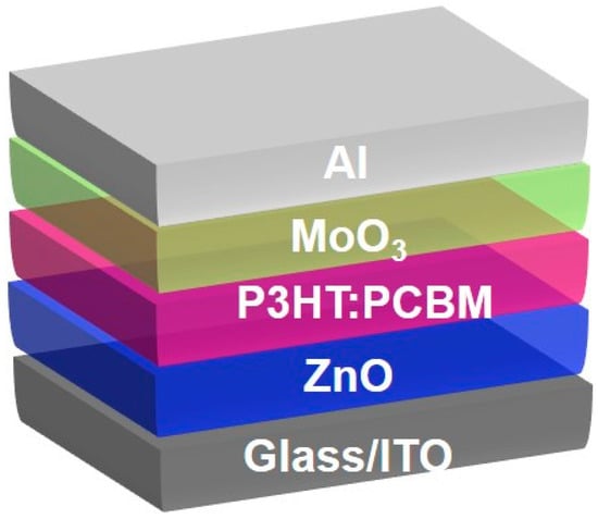
Figure 1.
Schematic device structure and energy band diagram of inverted P3HT:PCBM solar cells.
The photocurrent-voltage (J-V) curves under 100 mW/cm2 illumination from a solar simulator (Newport 91160A, AM 1.5G with a KG 5 filter) were taken in a vacuum closed-cycle refrigerator using a Keithley 237 source measuring unit. The incident photon to charge carrier efficiency (IPCE) spectra were measured by using a lock-in amplifier (Model 7265, Signal Recovery) when the devices were illuminated by monochromatic light from a xenon lamp through the monochromator (SpectroPro-150, Acton Research Corporation). The absorption spectra and XRD patterns were obtained using a DU-70 spectrophotometer (Beckman) and M18XHF-SR (MAC Science Co.). The surface morphology was investigated via non-contact atomic force microscopy (AFM, Park Systems XE-100). The impedance measurements (frequency range: 100 Hz to 10 MHz) were measured by an HP-4192A impedance analyzer.
3. Results and Discussion
Figure 2a shows the J-V characteristics for different annealing conditions under 100 mW/cm2 illumination. Different annealing conditions correspond to the non-treatment and 30 min of thermal annealing at 150 °C before (pre-annealing) and after the evaporation of MoO3/Al (post-annealing). The device characteristics depend on the annealing method, as shown in Figure 2 (see Table 1 for a summary of the results). Although VOC of the pre-annealed device decreases slightly, the corresponding short circuit current (JSC), fill factor (FF), and efficiency (8.78 mA/cm2, 0.55, and 3.03%, respectively) are significantly higher than those of the untreated device. The corresponding values of the post-annealed device (i.e., 7.36 mA/cm2, 0.46, and ~1.93%) are also higher than those of the untreated device, but lower than those of the pre-annealed device. RSH is related to the leakage current and RS is affected by the contact resistance between the active layer and the electrode. Therefore, the best condition (i.e., minimum RS and maximum RSH) is obtained in the pre-annealed device. Figure 2b shows the IPCE spectra for different annealing conditions. The maximum IPCE values of the non-annealed device and the pre-annealed device were 30% and 60% (corresponding to a JSC of 8.69 mA/cm2 for calculating the integral of IPCE and the AM1.5G reference spectrum), respectively, at 500 nm. The IPCE of the post-annealed device is ~5% lower, without any change in the spectral shape compared with that of the pre-annealed device. These results indicate that the performance difference between pre-annealing and post-annealing may have resulted from changes in the light absorption of the active layer and/or the charge carrier extraction in the device during the annealing process.
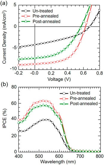
Figure 2.
(a) J-V curves obtained under 100 mW/cm2 illumination and (b) Incident photon to charge carrier efficiency (IPCE) spectra for different annealing conditions of the inverted P3HT:PCBM polymer solar cells.

Table 1.
Characteristics of P3HT:PCBM polymer solar cells for different annealing conditions under 100 mW/cm2 illumination.
The absorption spectra of P3HT:PCBM/MoO3 subjected to different annealing conditions are shown in Figure 3. All films were fabricated on quartz substrates and treated under different annealing conditions. The absorption spectra of the films change significantly after both annealing methods. The absorption spectrum of the un-treated film is characterized by a main peak at ~480 nm and a barely visible shoulder at ~600 nm. In the case of the pre-annealed and post-annealed films, the intensity associated with the main absorption peak increases significantly and the peak is red-shifted to ~500 nm. In contrast, the position of the shoulder peak remains almost unchanged. The absorbance of the post-annealed device seems to be better than that of the pre-annealed device (see Figure 3). However, this is the error range that occurs during the absorption measurement. In other words, the absorbance changes only slightly during the annealing sequence. This indicates that the evaporated MoO3 layer on the P3HT:PCBM before or after the annealing process has no effect on the light absorption of the P3HT:PCBM film. In principle, the absorbance property affects the device performance but does not always affect the device performance. That is, if the absorbance of light increases, a lot of charge will be generated, which helps to improve device performance. However, device performance is affected by light absorption and charge extraction properties are affected by the resistance inside the device and the morphology of the thin film. In other words, as Figure 3 shows, the absorption of pre-annealed devices and post-annealed devices is not much different, so absorption would not have a significant effect on JSC.
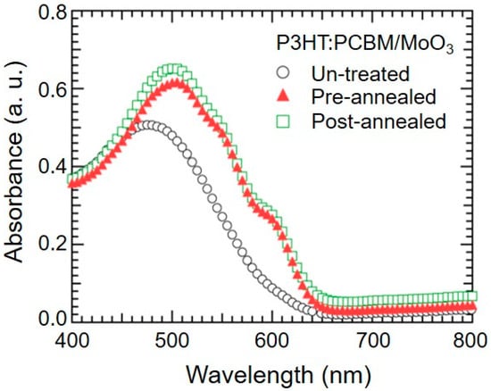
Figure 3.
Absorption spectra corresponding to different annealing conditions of P3HT:PCBM/MoO3 on quartz substrates.
Figure 4 shows the XRD patterns corresponding to different annealing conditions of P3HT:PCBM/MoO3 films on quartz substrates. The peak corresponding to crystalline P3HT occurs at 2θ = 5.4°. The height of the peak indicates the degree of P3HT crystallinity []. A weak peak occurs at 2θ = 5.45° in the XRD pattern of the un-treated P3HT:PCBM/MoO3. Although the height of the peak associated with the post-annealed film is slightly lower than that of the pre-annealed film, the XRD patterns of the pre-annealed and the post-annealed films appear similar. In both cases, the peak at 2θ = 5.3° is stronger than that of the untreated film. This result indicates that regardless of the annealing method, the P3HT crystallinity of the P3HT:PCBM film increases significantly with the thermal annealing process.
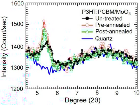
Figure 4.
XRD patterns for different annealing conditions of P3HT:PCBM/MoO3 on quartz substrates.
To compare the effect of the MoO3 layer during the annealing processes, the surface morphology and phase of P3HT:PCBM/MoO3 films (see Figure 5) subjected to pre-annealing and post-annealing processes were examined via non-contact AFM. The surface roughness of the post-annealed P3HT:PCBM/MoO3 film (i.e., 0.9 nm; Figure 5c) was considerably lower than that (1.8 nm) of the pre-annealed film (see Figure 5a). However, the corresponding phase images (Figure 5b,d) revealed that significantly finer MoO3 grains were formed in the post-annealed film than in the pre-annealed film. The results of previous studies on P3HT:PCBM films indicated that P3HT and PCBM in the bulk heterojunction film of P3HT:PCBM were self-organized during the annealing process [,,,,,]. This may have resulted from the fact that the evaporated MoO3 layer on the top of P3HT:PCBM was changed via self-organization of the P3HT:PCBM film during the post-annealing process. Therefore, we expect that compared with small grain sizes in the post-annealed film, larger grain sizes in the pre-annealed film allow (i) easy extraction of the generated charge carriers owing to a continuous path through the grain, and (ii) reduction of the carrier trapping by the disordered grain boundaries.
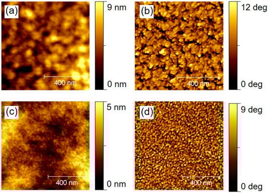
Figure 5.
Atomic force microscopy (AFM) images showing the pre-annealing [(a) morphology and (b) phase] and post-annealing [(c) morphology and (d) phase] of P3HT:PCBM/MoO3 films on quartz.
Figure 6 shows the Cole-Cole plots corresponding to different annealing conditions under the illumination of 100 mW/cm2. The plots consist of two semi-circles that occur at frequency values >50 kHz and frequency values <50 kHz. These plots were fitted by an equivalent circuit, which included constant phase elements (CPEs), as shown in the inset of Figure 6. The inhomogeneity of the material and/or the grain boundaries yield a non-ideal frequency-dependent capacitor. Therefore, compared with the RC-model, the CPE-model is better suited for plot-fitting of our devices []. The semi-circles are non-depressed regardless of the annealing conditions, and hence, similar values were obtained for the parallel resistances of CPE1 and CPE2. R2 and R3 values of ~2.3 and 10.8 Ω·cm2, respectively, were obtained (from the fitting curves) for the pre-annealed device under illumination. Values of 3.8 Ω·cm2 (R2) and 18.2 Ω·cm2 (R3) were obtained for the post-annealed device. This difference in resistances resulted from extracting the dissociated carriers in the active layer under illumination. Therefore, these results indicated that the resistance difference in the low-frequency range is derived from the MoO3 layer and the interface between the MoO3 and P3HT:PCBM layers when the device is treated under different conditions.
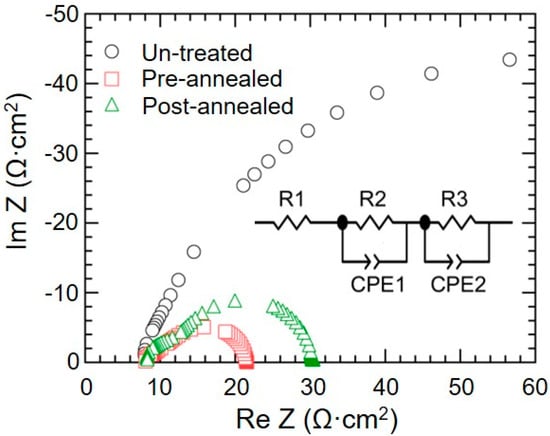
Figure 6.
Cole-Cole plots for different annealing conditions under 100 mW/cm2 illumination. The plots are calculated from the equivalent circuit (constant phase elements (CPEs) shown in the inset).
4. Conclusions
We demonstrated the inverted polymer solar cells for different annealing conditions of non-treatment, pre-annealing, and post-annealing under illumination. Regardless of the annealing method, the annealing process improved the light absorption ability and P3HT crystallinity of the P3HT:PCBM films. However, the performance of the pre-annealed device (3.03%) was superior to that (1.93%) of the post-annealed device. Moreover, compared with those of the post-annealed device, the better pre-annealing device resistances and large MoO3 grain size of the P3HT:PCBM contributed to improved charge transport by preventing carrier trapping in the grain boundaries. In other words, both the absorbance property and the charge extraction property affected the device and hence, the optimal performance was realized for the pre-annealed device. Therefore, compared with the post-annealing under the best conditions for the standard structure, we suggest that the pre-annealing process is more suitable for the inverted structure of P3HT:PCBM solar cells.
Funding
This work was supported by the National Research Foundation of Korea(NRF) grant funded by the Korea government(MSIT) (No. 2019R1G1A1100052).
Conflicts of Interest
The author declares no conflict of interest.
References
- He, Z.; Xiao, B.; Liu, F.; Wu, H.; Yang, Y.; Xiao, S.; Wang, C.; Russell, T.P.; Cao, Y. Single-junction polymer solar cells with high efficiency and photovoltage. Nat. Photonics 2015, 9, 174. [Google Scholar] [CrossRef]
- Lim, D.C.; Jeong, J.H.; Pyo, K.; Lee, D.; Heo, J.; Choi, J.W.; Lee, C.L.; Seo, J.; Kim, S.; Cho, S. Effect of emissive quantum cluster consisting of 22 Au atoms on the performance of semi-transparent plastic solar cells under low intensity illumination. Nano Energy 2018, 48, 518. [Google Scholar] [CrossRef]
- Meng, L.; Zhang, Y.; Wan, X.; Li, C.; Zhang, X.; Wang, Y.; Ke, X.; Xiao, Z.; Ding, L.; Xia, R.; et al. Organic and solution-processed tandem solar cells with 17.3% efficiency. Science 2018, 361, 1094. [Google Scholar] [CrossRef]
- Lee, S.; Park, K.H.; Lee, J.H.; Back, H.; Sung, M.J.; Lee, J.; Kim, J.; Kim, H.; Kim, Y.H.; Kwon, S.K.; et al. Achieving Thickness-Insensitive Morphology of the Photoactive Layer for Printable Organic Photovoltaic Cells via Side Chain Engineering in Nonfullerene Acceptors. Adv. Energy Mater. 2019, 9, 1900044. [Google Scholar] [CrossRef]
- Cheng, P.; Li, G.; Zhan, X.; Yang, Y. Next-generation organic photovoltaics based on non-fullerene acceptor. Nat. Photonics 2018, 12, 131. [Google Scholar] [CrossRef]
- Hou, J.; Inganäs, O.; Friend, R.H.; Gao, F. Organic solar cells based on non-fullerene acceptors. Nat. Mater. 2018, 17, 119. [Google Scholar] [CrossRef]
- Yuan, J.; Zhang, Y.; Zhou, L.; Zhang, G.; Yip, H.L.; Lau, T.K.; Lu, X.; Zhu, C.; Peng, H.; Johnson, P.A.; et al. Single-Junction Organic Solar Cell with over 15% Efficiency Using Fused-Ring Acceptor with Electron-Deficient Core. Joule 2019, 3, 1140. [Google Scholar] [CrossRef]
- Zhang, S.; Qin, Y.; Zhu, J.; Hou, J. Over 14% Efficiency in Polymer Solar Cells Enabled by a Chlorinated Polymer Donor. Adv. Mater. 2018, 30, 1800868. [Google Scholar] [CrossRef]
- Zhao, J.; Li, Y.; Yang, G.; Jiang, K.; Lin, H.; Ade, H.; Ma, W.; Yan, H. Efficient organic solar cells processed from hydrocarbon solvents. Nat. Energy 2016, 1, 15027. [Google Scholar] [CrossRef]
- Dennler, G.; Scharber, M.C.; Ameri, T.; Denk, P.; Forberich, K.; Waldauf, C.; Brabec, C.J. Design Rules for Donors in Bulk-Heterojunction Tandem Solar Cells Towards 15% Energy-Conversion Efficiency. Adv. Mater. 2008, 20, 579. [Google Scholar] [CrossRef]
- Chang, S.C.; Hsiao, Y.J.; Lin, T.C.; Li, T.S.; Zeng, S.A.; Yu, C.E. Improving Power Conversion Efficiency of P3HT/PCBM based Organic Solar Cells by Optimizing Graphene Doping Concentration and Annealing Temperature. Int. J. Electrochem. Sci. 2016, 11, 5819. [Google Scholar] [CrossRef]
- Darwis, D.; Sesa, E.; Farhamza, D. The Fabrication of Bulk Heterojunction P3HT: PCBM Organic Photovoltaics. Mater. Sci. Eng. 2018, 367, 012029. [Google Scholar] [CrossRef]
- Wang, W.; Guo, S.; Herzig, E.M.; Sarkar, K.; Schindler, M.; Magerl, D.; Philipp, M.; Perlich, J.; Müller-Buschbaum, P. Investigation of morphological degradation of P3HT: PCBM bulk heterojunction films exposed to long-term host solvent vapor. J. Mater. Chem. A 2016, 4, 3743. [Google Scholar] [CrossRef]
- Lee, H.; Kim, T.S.H. Combinatorial Effects of Solvent Type, Thermal Annealing and Al Electrode on the Morphology of P3HT: PCBM Layer. Sci. Adv. Mater. 2016, 8, 618. [Google Scholar] [CrossRef]
- Marumoto, K.; Kosuga, A.; Liu, D.; Takeuchi, O.; Shigekawa, H. Dependence of the Device Performance of Polymer Solar Cells on the Insertion of Metal Nanoparticle Layers at the Electron-collecting Electrodes. Electrochemistry 2017, 85, 272. [Google Scholar] [CrossRef]
- Kim, J.Y.; Kim, J.; Roh, J.; Kim, H.; Lee, C. Efficiency Improvement of Organic Photovoltaics Adopting Li- and Cd-Doped ZnO Electron Extraction Layer. IEEE J. Photovolt. 2016, 90, 930. [Google Scholar] [CrossRef]
- Kim, J.Y.; Cho, E.; Kim, J.; Shin, H.; Roh, J.; Thambidurai, M.; Kang, C.M.; Song, H.J.; Kim, S.; Kim, H.; et al. Improved photovoltaic performance of inverted polymer solar cells through a sol-gel processed Al-doped ZnO electron extraction layer. Opt. Express 2015, 23, 243417. [Google Scholar] [CrossRef]
- Wu, C.K.; Sivashanmugan, K.; Guo, T.F.; Wen, T.C. Enhancement of Inverted Polymer Solar Cells Performances Using Cetyltrimethylammonium-Bromide Modified ZnO. Materials 2015, 11, 243417. [Google Scholar] [CrossRef]
- Suman, C.K.; Noh, S.; Kim, S.; Lee, S.D.; Lee, C.; Lee, D.; Park, J. Electrical Impedance Studies of the Effect of a Buffer Layer on Organic Bulk Hetrojunction Solar Cells. J. Korean Phys. Soc. 2008, 53, 3278. [Google Scholar] [CrossRef]
- Mengistie, D.A.; Ibrahem, M.A.; Wang, P.C.; Chu, C.W. Highly Conductive PEDOT: PSS Treated with Formic Acid for ITO-Free Polymer Solar Cells. ACS Appl. Mater. Interfaces 2014, 6, 2292. [Google Scholar] [CrossRef]
- Madogni, V.I.; Kounouhéwa, B.; Akpo, A.; Agbomahéna, M.; Hounkpatin, S.A.; Awanou, C.N. Comparison of degradation mechanisms in organic photovoltaicdevices upon exposure to a temperate and a subequatorial climate. Chem. Phys. Lett. 2015, 640, 201. [Google Scholar] [CrossRef]
- Pacholski, C.; Kornowski, A.; Weller, H. Self-Assembly of ZnO: From Nanodots to Nanorods. Angew. Chem. Int. Ed. 2002, 41, 1188. [Google Scholar] [CrossRef]
- Tanaka, S.; Rosli, S.K.B.; Takada, K.; Taniai, N.; Yoshitomi, T.; Ando, H.; Matsumoto, K. Effects of bromination of poly(3-hexylthiophene) on the performance of bulk heterojunction solar cells. RCS Adv. 2017, 7, 46874. [Google Scholar] [CrossRef]
- Friesen, G.; Ozsar, M.E.; Dunlop, E.D. Impedance model for CdTe solar cells exhibiting constant phase element behavior. Thin Solid Film. 2018, 361, 303–308. [Google Scholar]
© 2019 by the author. Licensee MDPI, Basel, Switzerland. This article is an open access article distributed under the terms and conditions of the Creative Commons Attribution (CC BY) license (http://creativecommons.org/licenses/by/4.0/).