1. Introduction
Wireless power transfer (WPT) technologies have been rapidly developed and widely applied to many industrial applications, such as biomedical devices, consumer electronics, manufacturing facilities, and electric vehicles (Evs), where direct contact between power supplies and applications is impossible or inconvenient [
1,
2,
3,
4]. To efficiently transfer power, most of the WPT circuits use electromagnetic coupling between coils. These WPT circuits use capacitors to reduce reactive power [
5,
6,
7,
8,
9,
10,
11,
12,
13], and can be largely categorized into four types, depending on whether the capacitors are connected with the transmitter and receiver coils in series and series (S-S), series and parallel (S-P), parallel and parallel (P-P), or parallel and series (P-S) [
5,
6,
7]. Among them, the S-S circuit has been widely used because the capacitances can be chosen independently of the load and coupling conditions [
7,
8,
9,
10].
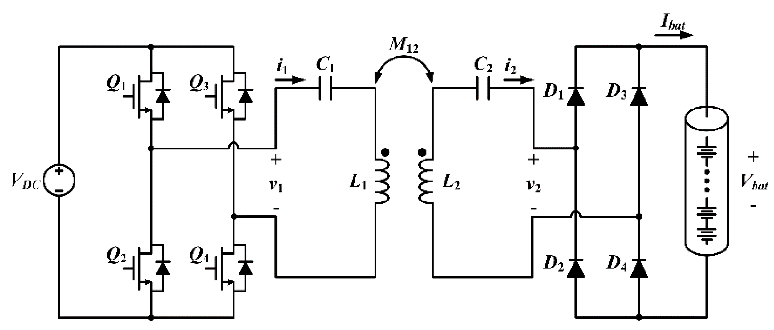
A typical S-S WPT circuit (
Figure 1) [
7,
9,
10] consists of a full-bridge inverter (
Q1–
Q4), a transmitter coil (
L1), a full-bridge rectifier (
D1–
D4), a receiver coil (
L2), and two capacitors (
C1 and
C2).
L1 forms a resonance circuit with
C1, and
L2 forms a resonance circuit with
C2. Both resonance circuits are designed to have the same resonance frequency
. The transmitter and receiver coils have a mutual inductance,
M12. The input to the full-bridge inverter is a DC voltage
VDC.
To charge a battery, the S-S WPT circuit should be operated in constant current (CC) output mode when the battery voltage
Vbat is lower than predetermined limit voltage
Vbat,cut, and in constant voltage (CV) mode when
Vbat,cut ≤
Vbat < charging voltage limit (CVL) [[
9,
10,
11,
12]. To support both modes, an additional DC–DC converter can be inserted between the S-S WPT circuit and the battery. However, the additional converter decreases the power transfer efficiency
ηe and the power density [
8,
13]. To solve this problem, the battery can be directly connected to the S-S WPT circuit, as in
Figure 1, and several control methods have been introduced [
9,
10,
11,
12,
13].
The WPT circuit in [
9] uses the same S-S WPT circuit (
Figure 1) and adopts a pulse frequency modulation (PFM) method to obtain a CV output. In this circuit, the switching frequency range should be selected differently whenever the coupling coefficient is varied, so the range of the frequency limiter cannot be determined easily when the coupling coefficient
k12 varies widely. Also, wireless communication should be introduced to operate the PFM method. The circuit in [
10] improves
ηe by using two intermediate coils that are placed between the transmitter and receiver coils, and uses
f =
fCC for CC output and
f =
fCV for CV output, where the frequencies
fCC and
fCV are determined by the coupling coefficients among the four coils. However, the values of
fCC and
fCV vary in the manner that any coupling coefficient varies, and no method has been developed to date to measure the coupling coefficients, so accurate determination of
fCC and
fCV is a difficult task. The circuits in [
11,
12] use auxiliary switches and capacitors to change the output from CC to CV mode. However, this circuit needs wireless communication to change the operational mode, and additional components also decrease the power density. As mentioned above, most of control methods require wireless communication to know the load conditions and coupling state.
To eliminate the necessity for wireless communication, several load estimation methods have been presented [
14,
15,
16,
17,
18,
19]. The methods in [
14,
15,
16] predict the load resistance
RL by using the information of the input voltage and current. However, these methods should know the value of the coupling state before estimating the load conditions, so they cannot be used for various coil alignments. The method in [
17] adopts an additional capacitor in the S-S WPT circuit; this method operates the circuit in two modes for system identification, and analyzes the reflected impedance. However, the additional capacitor and bidirectional switch increase the circuit cost. The method in [
18] measures the input voltage and current, and separates the imaginary part of the input impedance. To estimate the load conditions and coupling state, this method is implemented at one frequency, which is not a resonant frequency, so the impedance of the resonant tank slightly decreases the power transfer efficiency. The method in [
19] injects a high frequency energy into the S-S WPT circuit, then detects the response of the circuit to estimate the load conditions. However, this method cannot follow the load conditions after initial energy injection. All of these methods [
14,
15,
16,
17,
18,
19] can estimate the load conditions well, so they should be able to sense the high-frequency AC input voltage and current. The resonant frequency of the WPT circuit can be up to several hundred kilohertz, so the sampling frequency should be much higher than the resonant frequency; as a result, the analog-to-digital conversion is difficult.
This paper proposes a wireless battery charging circuit along with a load estimation method. This circuit does not need any wireless communication between the transmitter and receiver sides, and predicts the load resistance
RL, output voltage
Vbat, output current
Ibat, and mutual inductance
M12. In addition, because the simple peak current detection circuit is applied at the transmitter coil, the proposed circuit only senses the DC value, and does not need a high sampling frequency. The proposed WPT circuit senses the peak current values of the transmitter coil at
fo and auxiliary frequency
fa, and calculates the load conditions by using these values. Then, the proposed WPT circuit operates in CC and CV modes, depending on the estimated load conditions and phase shift control of the full-bridge inverter. In
Section 2, the analysis of the proposed WPT circuit with a load estimation method is given based on the fundamental harmonic approximation (FHA), experimental results are presented in
Section 3, possible errors in the proposed estimation method are analyzed in
Section 4, and a conclusion is given in
Section 5.
2. Wireless Power Transfer Circuit for Battery Charging
2.1. Theoretical Models of the S-S WPT Circuit
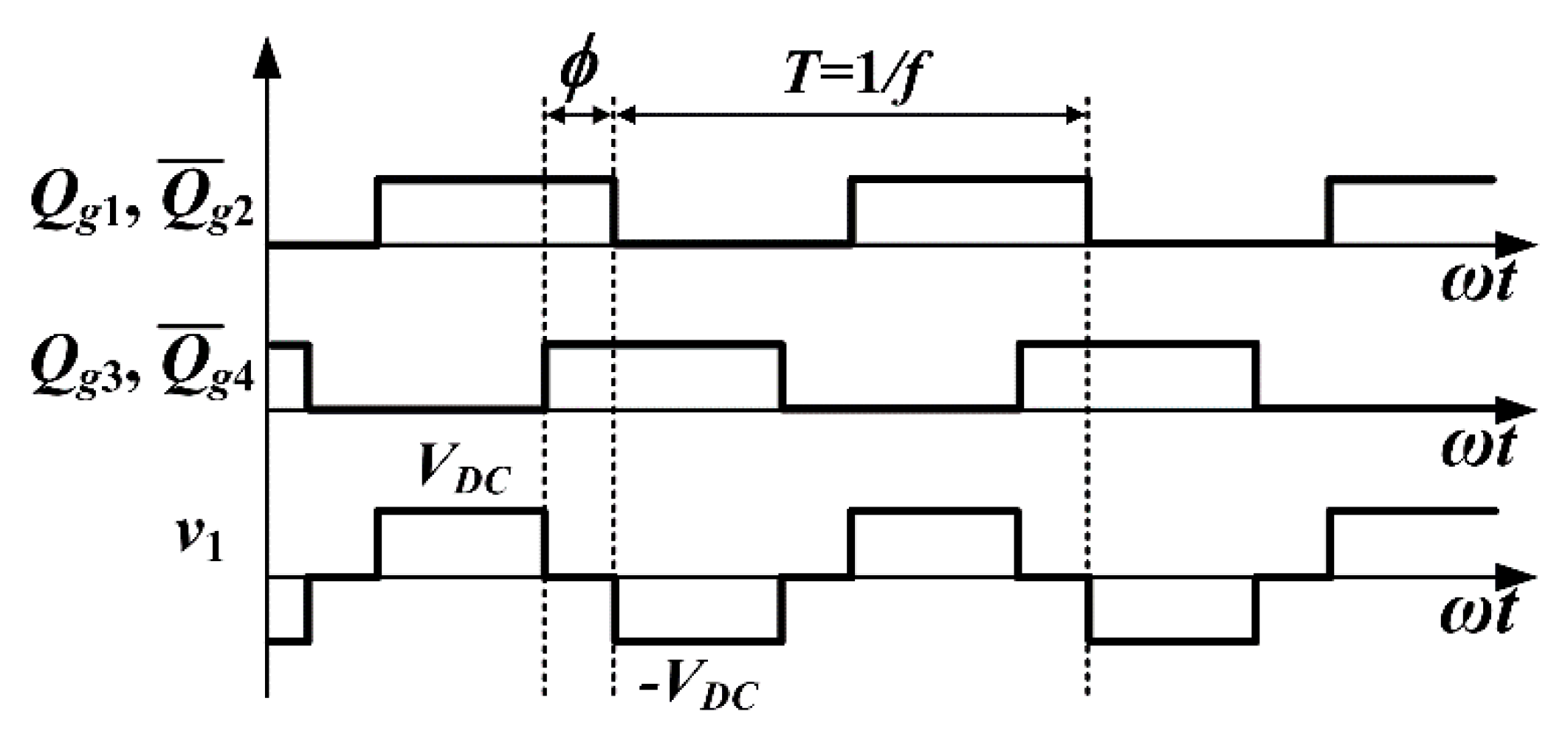
The gate control pulses
Qg1–
Qg4 (
Figure 2) for the full-bridge inverter have a switching frequency
f = 1/
T =
ω/(2
π). The switching phase of
and
lags behind that of
lags behind that of and
by an angle
ϕ, so the bipolar output pulses of the full-bridge inverter (
v1,
Figure 2) have a dead phase angle
ϕ between the pulses. The fundamental component of
v1 is given by
The current
i1(
t) of the transmitter coil, the current
i2(
t) of the receiver coil, and the input voltage
v2(
t) to the rectifier in
Figure 1 can be expressed as
where
θ and
ϕ are phase angles,
Vbat is the battery voltage, and
Ibat is the averaged charging current of the battery.
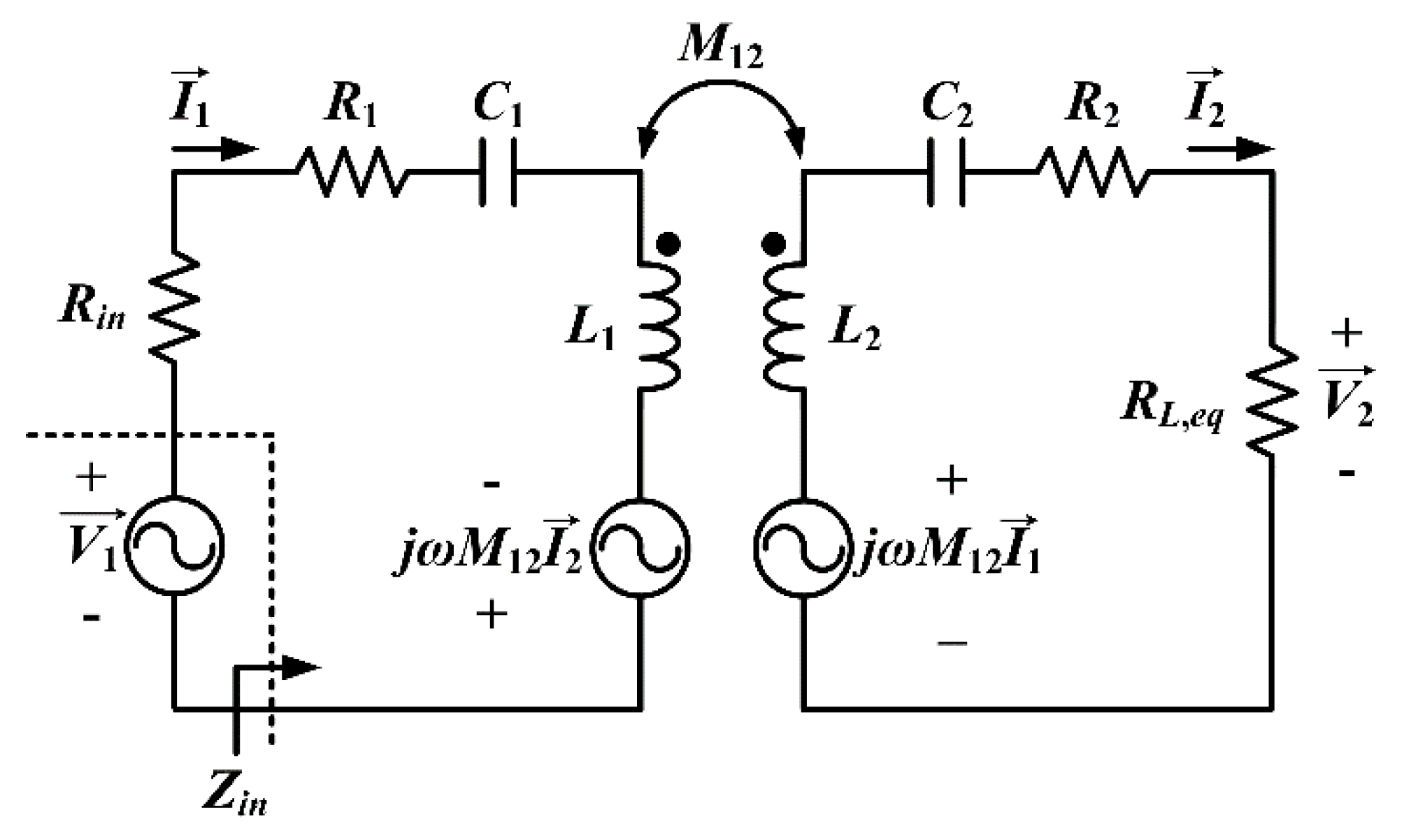
The S-S WPT circuit had an equivalent circuit (
Figure 3) for the fundamental component, where
Rin,
R1, and
R2 are the equivalent series resistances (ESRs) of the full-bridge inverter, primary coil, and secondary coil, respectively. Using Equations (3) and (4), the equivalent resistance of the battery
Rbat can be modeled with an equivalent resistance
RL,eq as:
Then, the Kirchhoff’s voltage law (KVL) gives
where
Z1 =
R1 +
jωL1 + 1/(
jωC1) and
Z2 =
R2 +
jωL2 + 1/(
jωC2). Using Equations (6) and (7), the phase of the input impedance
Zin (
Figure 4a), the voltage conversion ratio
Tv (
Figure 4b), the amplitude of
i1(
t), the peak current of
i1(t) (
I1) (
Figure 4c), the amplitude of
i2(
t), and the peak current of
i2(t) (
I2) (
Figure 4d) are calculated as
2.2. Load Estimation Method Using the Magnitue of Input Impedance
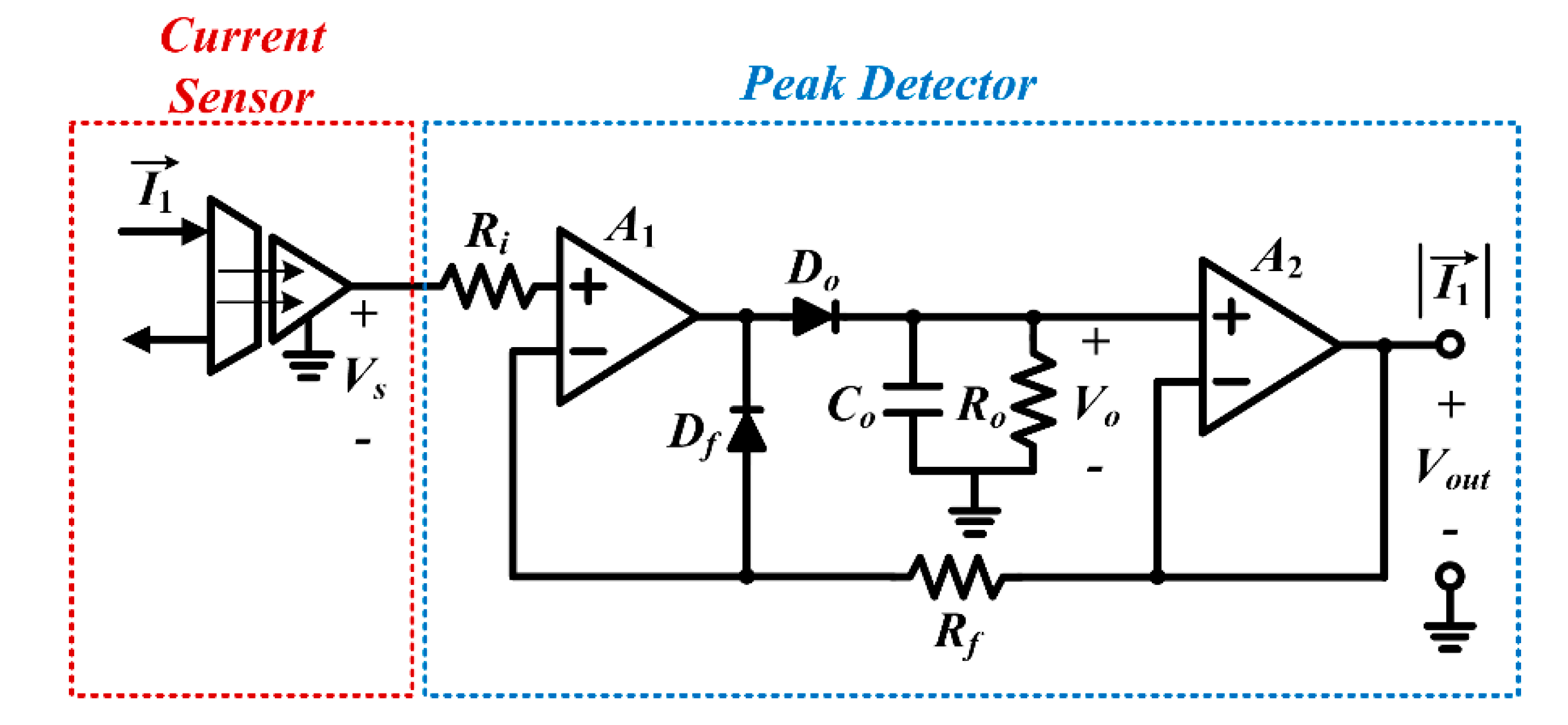
The proposed circuit uses the simple peak detection circuit (
Figure 5) in [
20] to measure the peak current of the transmitter coil
I1 as a DC value. The peak detection circuit is composed of a current sensor, an amplifier for the peak detection (
A1), an amplifier for the voltage follower (
A2), an input resistance of peak detector (
Ri), a feedback loop resistance (
Rf), a feedback loop diode (
Df), a rectification diode (
Do), an output capacitor (
Co), and an output resistance (
Ro). If the output voltage of the current sensor (
Vs) is lower than the voltage of
Co (
Vo),
Df remains on, and
Do remains off. In this operating mode, the output voltage of
A2 (
Vout) is clamped to
Vo, and
Co is discharged by
Ro. When
Vo becomes smaller than
Vs,
Df is turned off and
Do is turned on. In this operating mode,
Co is charged to the new positive peak of
Vs, so
Vs =
Vo =
Vout.
To estimate the load conditions, the peak detection circuit measures the peak current I1,o at f = fo and I1,a at f = fa, respectively, and uses simple mathematical equations for the input impedance. The measurement time of I1,o and I1,a is short, so the load conditions are assumed to remain constant during the estimation process. Also, the system parameters of the transmitter side (VDC, ϕ, L1, C1 and R1) and receiver side (L2, C2 and R2) are assumed to be known, and the proposed method predicts M12, RL,eq, Ibat, and Vbat.
At first, the circuit operates at
f =
fo, and the
M12 can be expressed using detected
I1,o and Equation (8) as
where
V1,o is the peak voltage of the transmitter coil at
f =
fo,
from Equation (1), and the unknown parameters of Equation (12) are
M12 and
RL,eq.
Then, the circuit operates at
f =
fa, and the square of the absolute value of input impedance
can be expressed using Equation (8) as
where
V1,a,
I1,a is the peak voltage and current of transmitter coil at
f =
fa,
from Equation (1). In this equation, the unknown parameters are the same as Equation (12).
If Equation (12) is applied to Equation (13), the
RL,eq can be arranged as
, where
α,
β and
γ are as follows:
This equation has two solutions for
RL,eq, and the smaller one is a reasonable value according to the calculation result, so estimated load resistance
RL,eq,est and estimated equivalent resistance of battery
Rbat,est can be estimated as
Then, the estimated mutual inductance
M12,est can also be derived by applying Equation (17) to Equation (12) as:
Other important estimated load parameters
Ibat,est and
Vbat,est at
f =
fo can be expressed using Equations (1)–(7), (17), and (18) as
Finally, the proposed method can predict
RL,eq,
M12,
Ibat, and
Vbat, and does not need a high sampling frequency to measure AC voltage and current, similar to previous studies [
14,
15,
16,
17,
18,
19].
2.3. Control Method of the S-S WPT Circuit for Battery Charging
The battery should be charged in CC mode when
Vbat ≤
Vbat,cut, and in CV mode when
Vbat >
Vbat,cut. In CV mode,
Ibat decreases as
Vbat increases, until
Ibat reaches the end charging current
Iend at which the charging operation stops [
9,
10,
11,
12].
Tv and
I2 in Equations (9) and (11) depend on
RL,eq, which varies as the charge state of battery varies. When all ESRs are negligibly small, Equation (11) gives
I2 at
ω =
ωo as
because
Z1 =
R1 and
Z2 =
R2 when
ω =
ωo. This equation indicates that the WPT circuit can be operated in CC mode if all ESRs are ignored and
ω =
ωo. However, ESRs affect the capability of CC regulation (
Figure 4d), so a separate control method should be introduced to attain CC mode; the proposed WPT circuit applies phase shift control of the full-bridge inverter at
f =
fo, and the
ϕ to maintain the CC output is compensated by using the proportional integral (PI) controller, which can be calculated as
where
Iref is the predetermined charging current reference. If ESRs are very small in CC mode, the influence of
RL,eq in
ϕ will also be very small.
To operate the WPT circuit in CV mode,
Tv should not depend on
RL,eq. If all ESRs are negligible, Equation (9) can be approximated as
where
. After setting
κ = 0, the frequencies
fCV1 and
fCV2 for CV operation are obtained as
and
, and
Tv at
f =
fCV1 or
f =
fCV2 is calculated using Equation (23) and
as
. However, ESRs in CV mode are also difficult to ignore, and if
fCV1 and
fCV2 deviate too much from
fo, the system efficiency also drastically decreases [
14]. Therefore, the proposed WPT circuit still operates at
f =
fo in CV mode, and the
ϕ to maintain the CV output is compensated by using the PI controller, which can be calculated as
The influence of RL,eq in CV mode cannot be ignored, even if ESRs are very small. Thus, ϕ will increase as RL,eq increases.
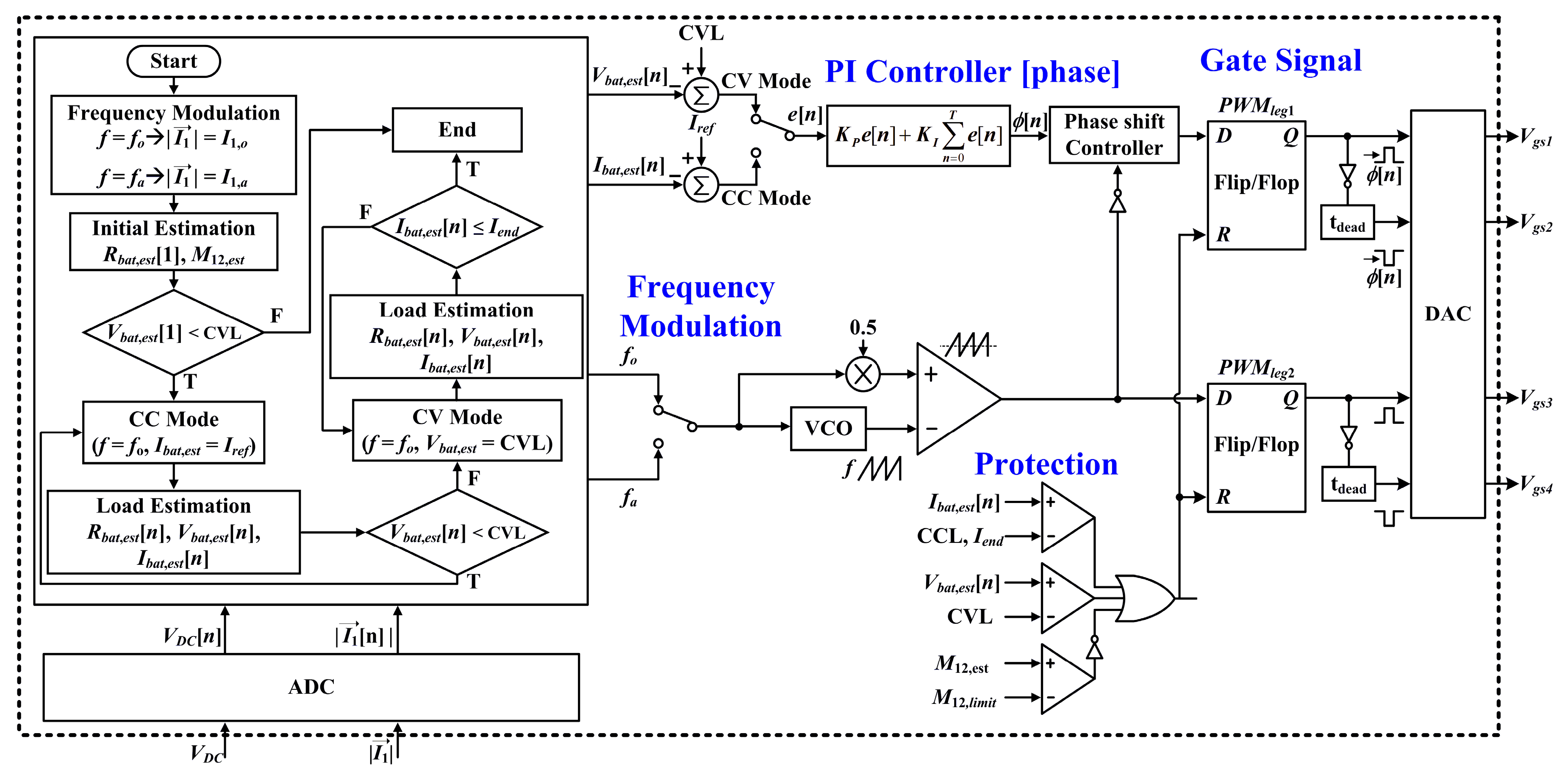
Finally, the proposed S-S WPT circuit applies the control algorithm (
Figure 6) for battery charging, and it consists of the following procedures:
- (1)
Modulate the WPT circuit at f = fo and fa; sense the I1,o and I1,a, respectively.
- (2)
Using the I1,o and I1,a, estimate Rbat,est[1] = Vbat,est[1] / Ibat,est[1] and M12,est.
- (3)
If Vbat,est[1] < CVL, begin the control procedure. Otherwise, turn off the S-S WPT circuit.
- (4)
Set f = fo to operate the WPT circuit in the CC mode.
- (5)
Using the PI controller, adjust ϕ[n] such that Ibat,est equals to Iref.
- (6)
Estimate the Rbat,est[n] = Vbat,est[n] / Ibat,est[n] by using I1,o[n] and (12); Rbat,est[n] is continuously updated to follow the charging profile of battery.
- (7)
Repeat (5)–(6) until Vbat,est[n] = CVL.
- (8)
Change the operation of WPT circuit from the CC to CV mode, and maintain f = fo.
- (9)
Using the PI controller, adjust ϕ[n] such that Vbat,est = CVL.
- (10)
Repeat procedure 6 until Ibat,est[n] =Iend.
- (11)
Turn off the S-S WPT circuit.
The controller has a protection function for charging current limit (CCL), CVL, and coil alignment of the WPT circuit. When M12,est < M12,limit, the controller terminates the battery-charging operation, because the alignment of the coils is inappropriate for battery charging.
3. Experimental Results
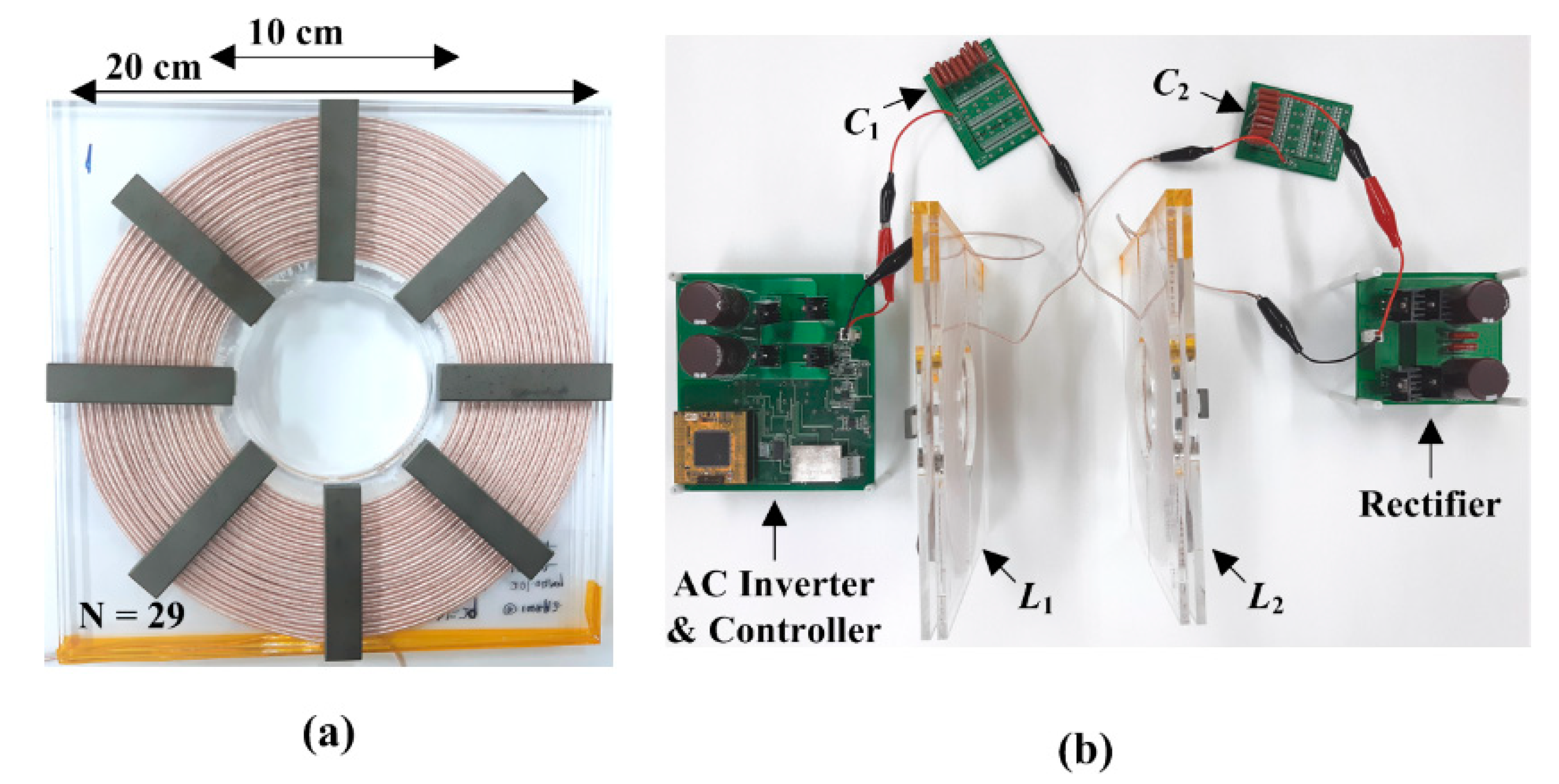
The experimental S-S WPT circuit for battery charging (
Figure 7a,b) was built and tested to prove the proposed control method. Two identical coils had an inner diameter of 100 mm and outer diameter of 200 mm;
L1 = 202.49 μH,
L2 = 202.06 μH, and
C1 =
C2 = 50 nF were chosen for
fo = 50 kHz. The input voltage
VDC was 50 V, and the sampling frequency to sense the output value of the peak detector was set as 50 kHz, which was simply synchronized to the
fo. The values of circuit parameters are given in
Table 1.
First, the load estimation was performed using the method in
Section 2.2.
Rbat and
M12 between the transmitter and receiver coils were measured and estimated using electrical load (DL1000H; NF, Co., Ltd.) and a inductance, capacitance and resistance (LCR) meter. The coil alignment was modulated on either the separation
h in the axial direction of the coil or the misalignment
v in the radial direction (
Figure 8). At
h = 6 cm and
v = 0 cm, the WPT circuit was operated at
fo = 50 kHz and
fa = 55 kHz to estimate the load condition, and
Rbat = 20.11 Ω and
M12 = 48.81 μH at
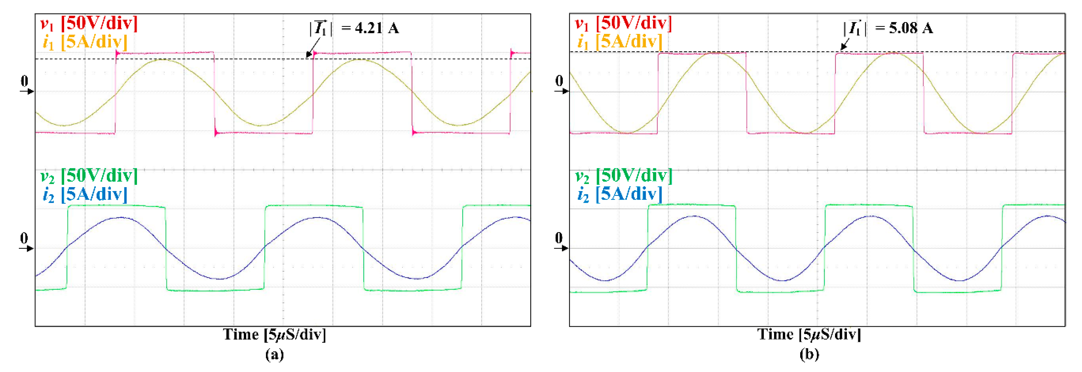
ϕ = 0. The measured
I1,o = 4.21 A (
Figure 9a) and
I1,a = 5.08 A (
Figure 9b), and the estimated load conditions were
Rbat,est = 20.49 Ω and
M12,est = 49.30 μH by using Equations (17) and (18). The errors of estimation results were −1.88% and −1.86%, respectively; other estimation results were obtained while varying
h,
v, and
Rbat (
Table 2 and
Table 3). Here,
h was varied in the range of 5–7 cm at
v = 0 cm,
v was varied in the range of 0–6 cm at
h = 0 cm, and
Rbat was varied in the range of 15.06–25.17 Ω. As a result, the proposed method estimated the
Rbat and
M12 within absolute errors at <3.87% and <3.38%, respectively. These experimental results demonstrate the usefulness of the proposed load estimation method. The errors of estimation were caused by inductance variation according to the coil alignment conditions and measurement error at
fo and
fa. A detailed error analysis is given in the next section.
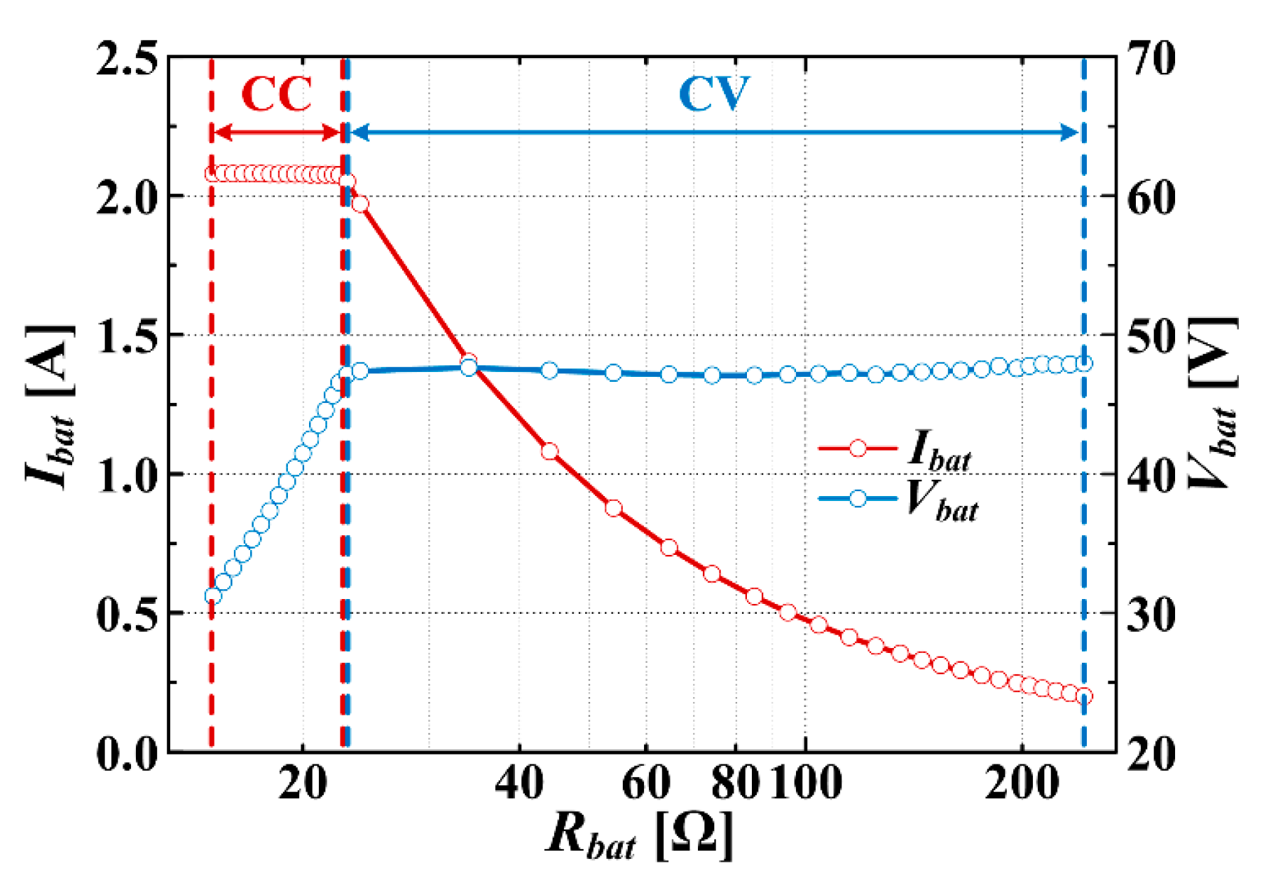
The current and voltage regulation for the battery charging were implemented using the controller proposed in
Section 2.3. An electrical load was used to emulate the battery pack, which was assumed to have 30 V ≤
Vbat ≤ 48 V (corresponding to a pack of 12 serially connected Li-ion battery cells). The
Rbat of the battery pack was 15 Ω ≤
Rbat ≤ 24 Ω for CC charging at
Iref = 2 A and 24 Ω ≤
Rbat ≤ 240 Ω for CV charging at CVL = 48 V and
Iend = 200 mA. The transmitter and receiver coils were located at
h = 5 cm and
v = 0 cm. In procedures 1 and 2, the controller of the WPT circuit used
fo = 50 kHz and
fa = 55 kHz;
Rbat,est (1) = 15.51 Ω at
Rbat = 15.01 Ω (−3.33% error) and
M12,est = 59.78 μH at
M12 =59.18 μH (−1.01% error). Because
Vbat,est (1) = 31.02 V < CVL in procedure 3, the controller began the charging control procedures in steps 4–11.
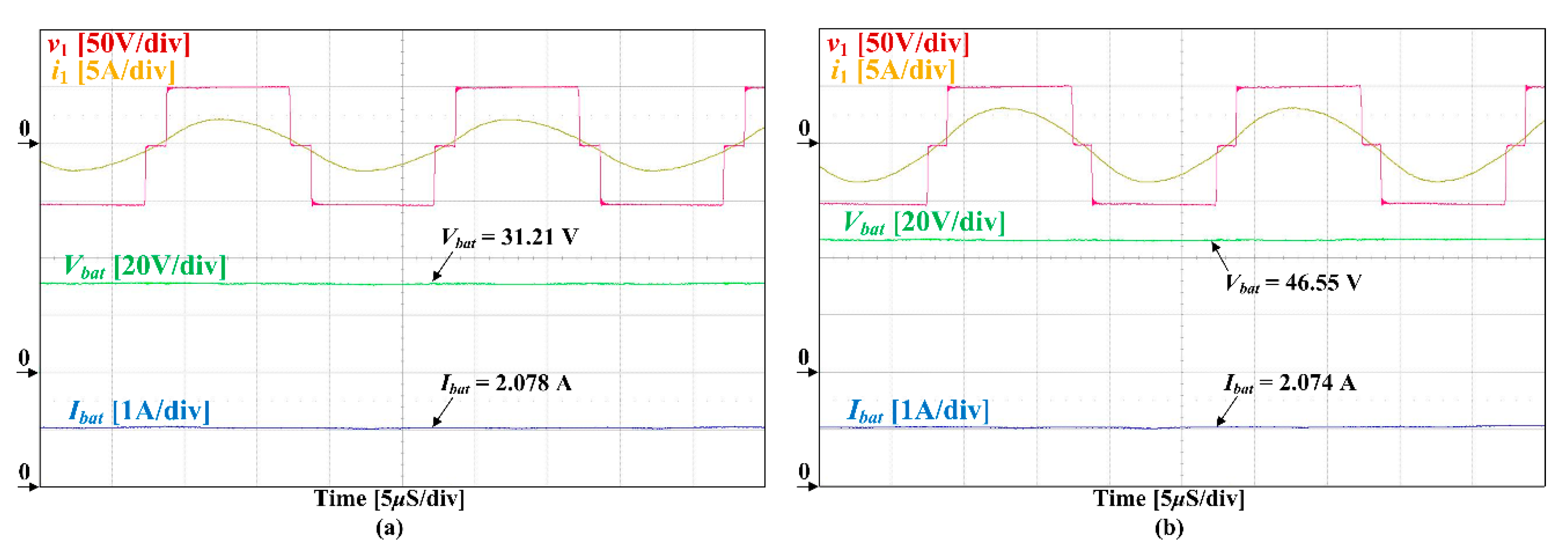
In the CC mode of procedures 4–7, the waveform (
Figure 10) shows that
v1 and
i1 had the same phase because the S-S WPT circuit operated at
f =
fo, and that
ϕ was compensated to regulate
Ibat,est =
Iref. When the circuit operated at
Rbat = 15.01 Ω (
Figure 10a),
Ibat = 2.07 A (–3.5% error) and
Vbat = 31.21 V. In this CC mode,
Vbat increased as
Rbat increased because
Ibat,est tracked the predetermined
Iref = 2 A. The waveform of
Figure 10b shows that
Vbat increased to 46.55 V at
Rbat = 22.47 Ω, while
Ibat = 2.07 A (–3.5% error). When procedure 5 was used in the CC mode, the range of regulated
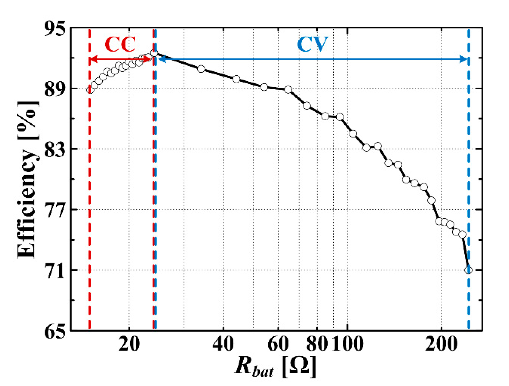
Ibat was 2.074–2.079 A; the tracking absolute error was <3.95% (Figure 12). The power transfer efficiency of the CC mode gradually increased as
Rbat increased, and the range of it was 88.81–92.05% (Figure 13). After
Vbat,est reached CVL = 48 V, the charging mode was changed to CV mode in the procedures 8–11.
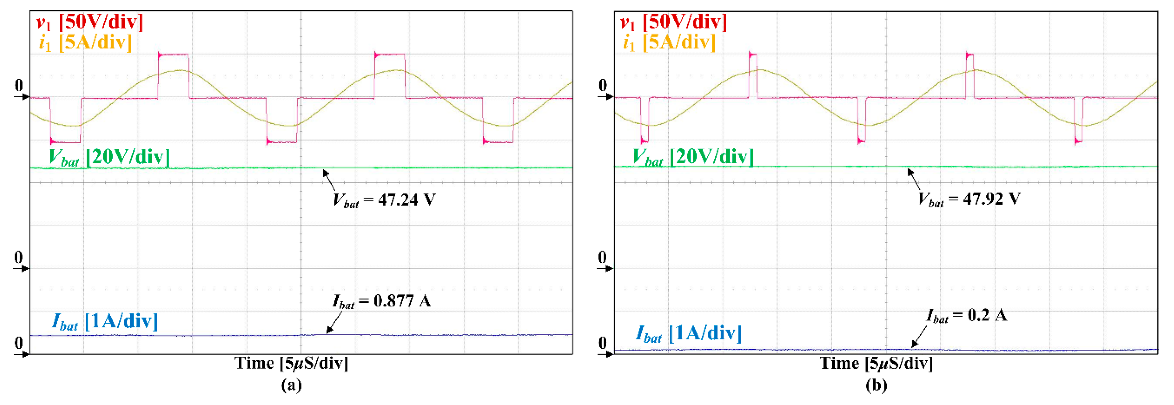
The waveform of CV mode (
Figure 11) also shows that
v1 and
i1 had the same phase because the S-S WPT circuit operated at
f =
fo, and that
ϕ was compensated to regulate
Vbat,est = CVL. When the circuit operated at
Rbat = 54.10 Ω (
Figure 11a),
Vbat = 47.24 V (1.58% error) and
Ibat = 0.88 A. In this CV mode, as
Rbat increased,
Tv increased (
Figure 4b);
ϕ should be increased to maintain
Vbat. Thus,
Ibat gradually decreased until
Ibat,est =
Iend. The waveform of
Figure 11b shows that
Ibat decreased to 0.2 A at
Rbat = 244 Ω, while
Vbat = 47.92 V (0.16% error). When procedure 9 was used, the range of regulated
Vbat was 47.09–47.92 V; the tracking absolute error was <1.89% (
Figure 12). The power transfer efficiency of the CV mode gradually decreased as
Rbat increased, and the range was 74.77–92.49% (
Figure 13).
These results show that the proposed load estimation method is suitable for use in battery charging, and that the adjustment of ϕ was crucial to have Ibat follow Iref in CC charging mode and to have Vbat follow CVL in CV charging mode.
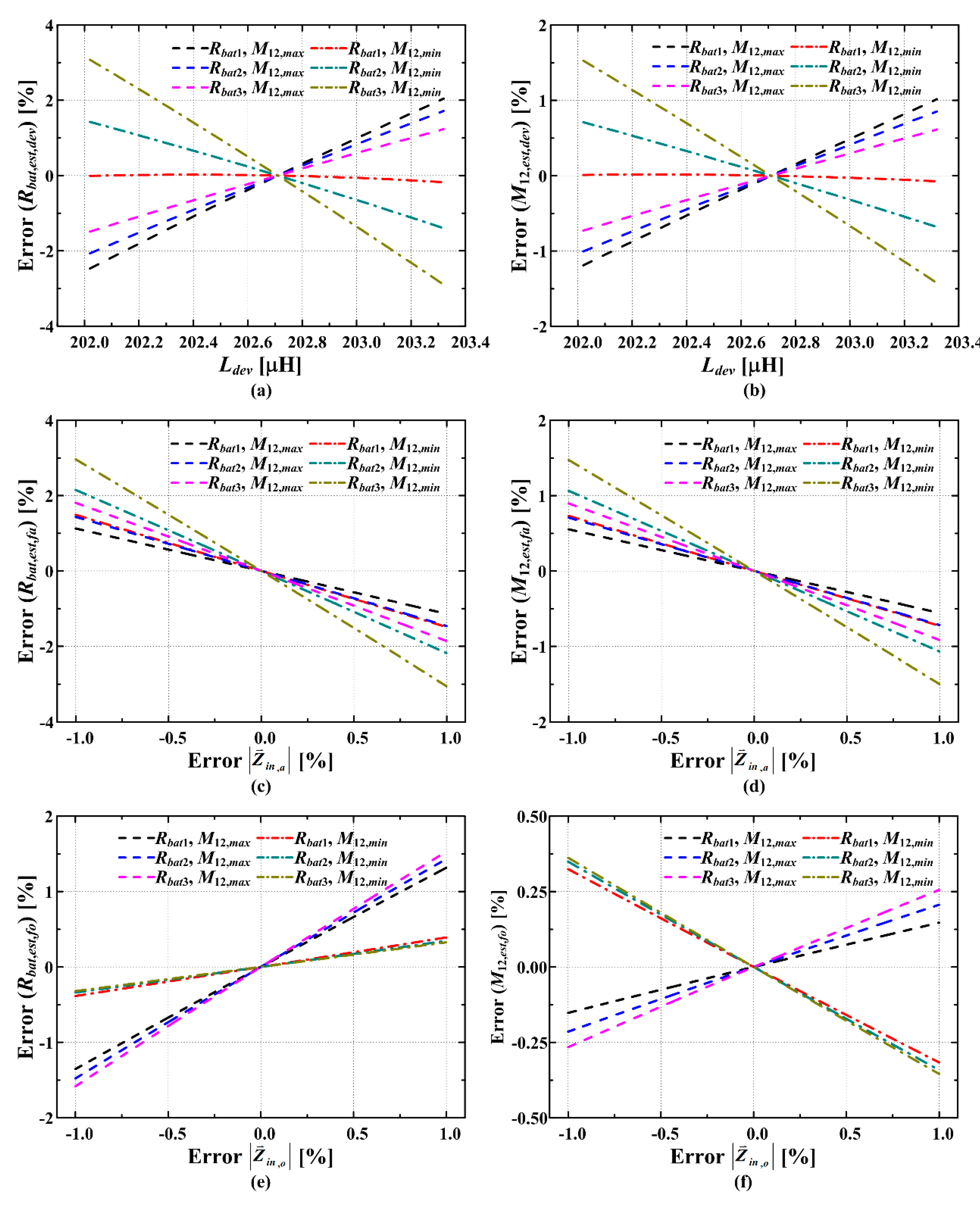
4. Error Analysis
In the proposed estimation method, the errors of estimation results can be generated using the deviated inductance (Ldev) according to the coil alignment and measurement error of input impedance at fo and fa. Therefore, these errors of the proposed method were analyzed by using MATLAB (R2015a, MathWorks, Massachusetts, USA) in this section.
In this section, the errors of estimation results due to the
Ldev (
Figure 14a,b) were calculated as
where
Rbat,est(
Ldev) and
M12,est(
Ldev) are estimated
Rbat and
M12 in the
Ldev. The measurement errors of input impedance (
Figure 14c–f) were calculated as
where
and
are measured values of
and
at
f =
fa and
f =
fo by using a peak detection circuit in
Figure 5. Then, the errors of estimation results due to the
and
(
Figure 14c–f) were calculated as
where
Rbat,est(
) and
M12,est(
) are
Rbat,est and
M12,est in the
, and
Rbat,est(
) and
M12,est(
) are
Rbat,est and
M12,est in the
.
At first, the coil alignment of the proposed estimation method was verified in the rage of
h = 5–7 cm at
v = 0 cm and
v = 0–6 cm at
v = 5 cm. In this misalignment range of coils, the self-inductance of
L1 and
L2 was changed according to the effect of the magnetic field between coils. The variation range of
L1 = 202.01–203.41 μH, and
L2 = 201.50–202.94 μH in
M12 = 38.66–59.18 μH. In this error analysis, according to the
Ldev, the simulation parameters were set as
L1 =
L2 = 202.71 μH,
C1 =
C2 = 49.97 nF,
Rin = 12 mΩ,
R1 = 252 mΩ, and
R2 = 248 mΩ. Then, the
Ldev was equivalently set between
L1 and
L2 as
Ldev =
L1,dev =
L2,dev = 202.02–203.41 μH,
Rbat1 = 15 Ω,
Rbat2 = 20 Ω,
Rbat3 = 25 Ω,
M12,max = 59.18 μH, and
M12,min = 38.66 μH. The
and
were set to zero in this analysis, and only
Ldev was considered. As a result, the Error(
Rbat,est,dev) and Error(
M12,est,dev) increased as
Rbat decreased at
M12,max and
Rbat increased at
M12,min (
Figure 14a,b). Also, the Error(
Rbat,est,dev) and Error(
M12,est,dev) due to the variation of
Rbat (
Rbat1–
Rbat3) were more sensitive at
M12,min than
M12,max.
Secondly, the proposed estimation method measures the
and
, and the
and
have an effect on the accuracy of the estimation. In this error analysis, according to the
and
, Error(
Rbat,est,fa), Error(
M12,est,fa), Error(
Rbat,est,fo), and Error(
M12,est,fo) were analyzed under the ±1% variation of
and
, and the simulation parameters were equivalently set as the error analysis of Equations (25) and (26). The Error(
Rbat,est,dev) and Error(
M12,est,dev) were set to zero in this analysis. In the
, the Error(
Rbat,est,fa) and Error(
M12,est,fa) increased as
Rbat increased, and were larger at
M12,min than
M12,max in the same
Rbat (
Figure 14c,d). In the
at
M12,max, the Error(
Rbat,est,fo) and Error(
M12,est,fo) increased as
Rbat increased. At
M12,min, the Error(
Rbat,est,fo) increased as
Rbat decreased, and Error(
M12,est,fo) increased as
Rbat increased (
Figure 14e,f). Overall, the
had more impact on the accuracy of proposed estimation method than the
.
In conclusion, the errors of estimation results were <3% in Equations (25), (29), and (31), and <1.5% in Equations (26), (30) and (32). Also, Equations (25) and (26) (
Figure 14a,b) were more sensitive to the variation of
Rbat and
M12 than Equations (29)–(32) (
Figure 14c–f). In the practical applications, the proposed controller (
Figure 6) includes the protection function to limit the range of coil alignment as
M12,est <
M12,limit, and the auxiliary positioning device can be introduced to minimize the inductance deviation.


