Reduction of DC Current Ripples by Virtual Space Vector Modulation for Three-Phase AC–DC Matrix Converters


Abstract
:1. Introduction
2. Topology and Modulations of AC–DC Matrix Converter
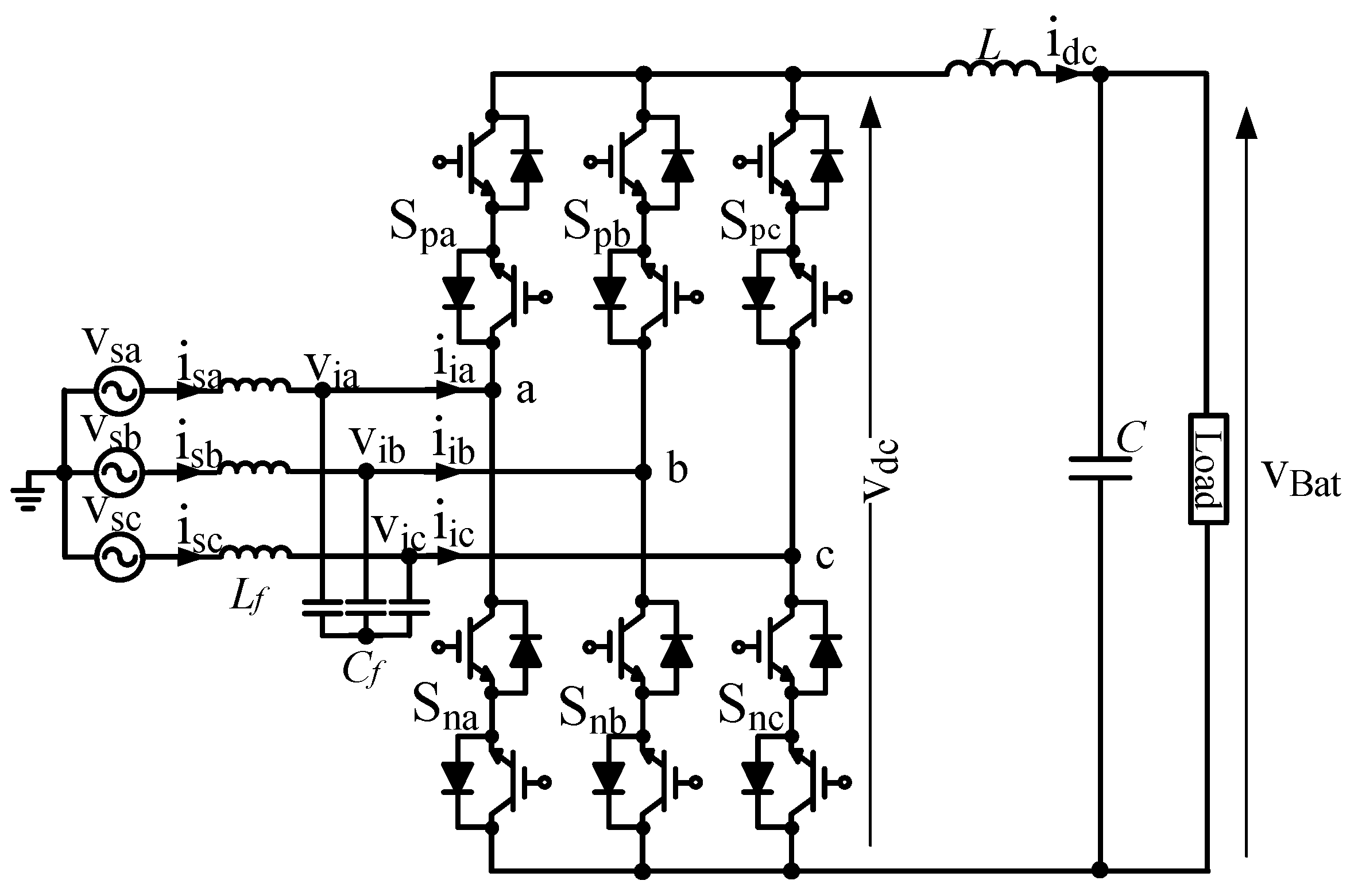
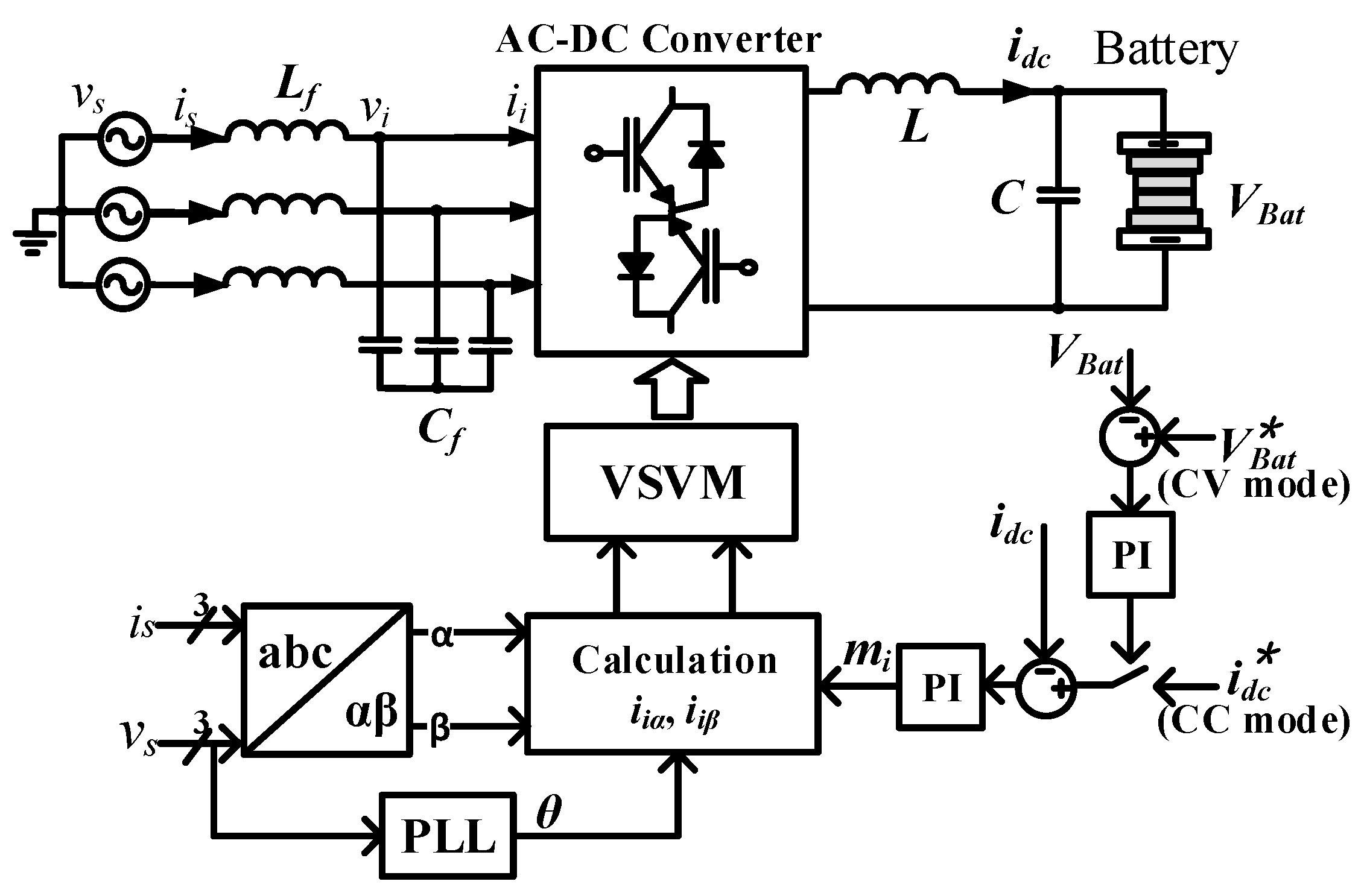
2.1. The Topology of AC–DC Matrix Converter
2.2. Modulations of AC–DC Matrix Converter
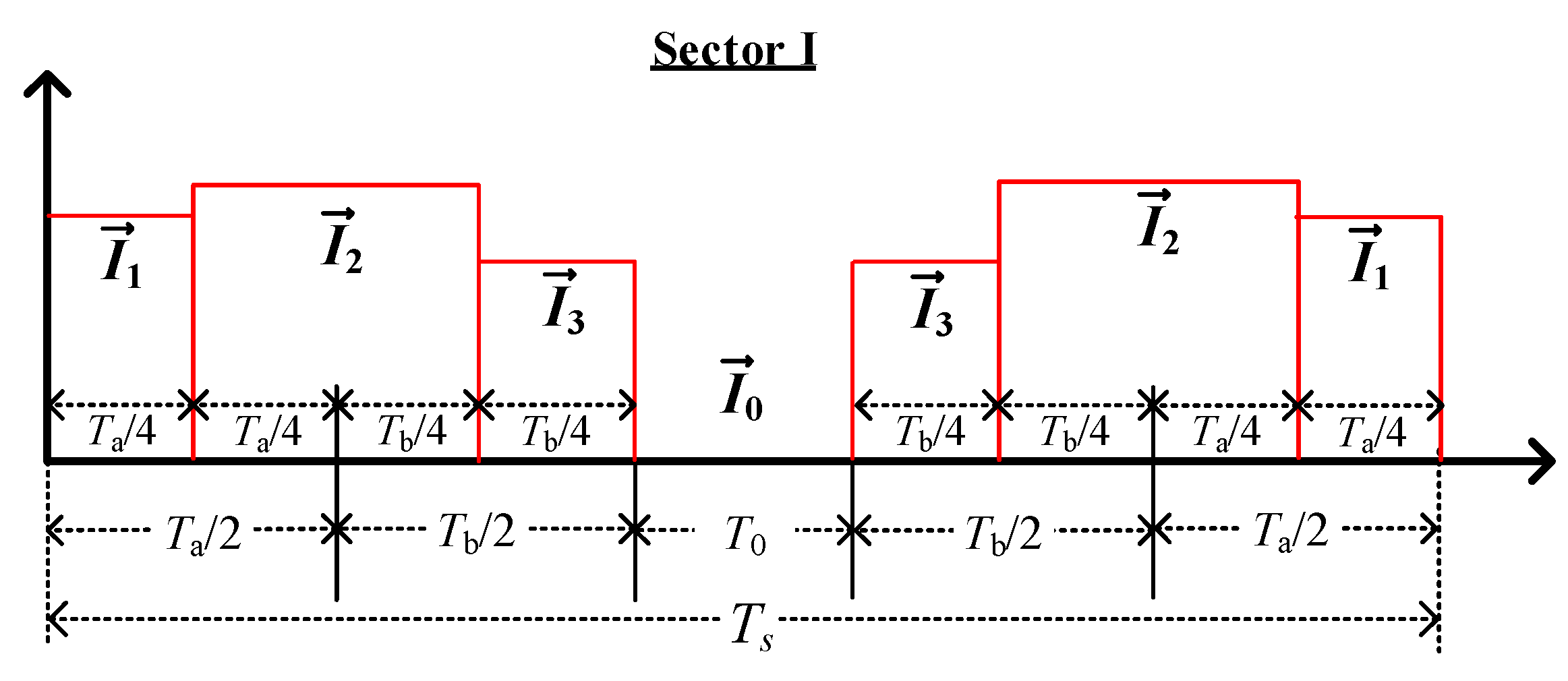
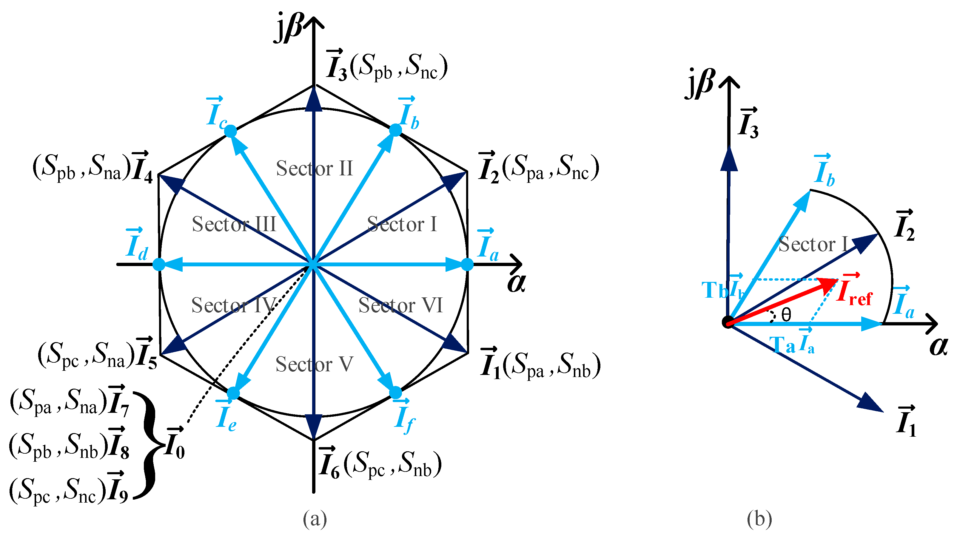
2.2.1. Conventional Space Vector Modulation
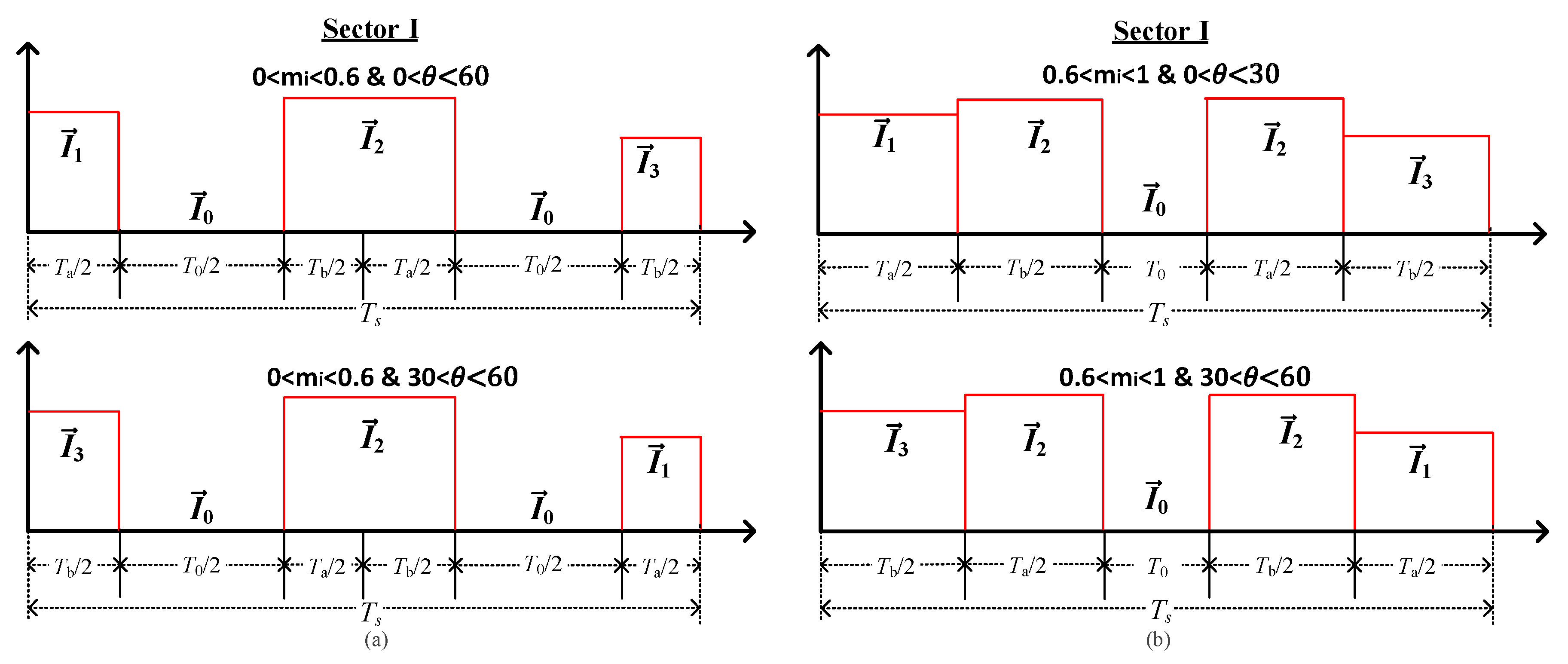
2.2.2. Proposed Virtual Space Vector Modulation
3. DC Current Ripple Analysis
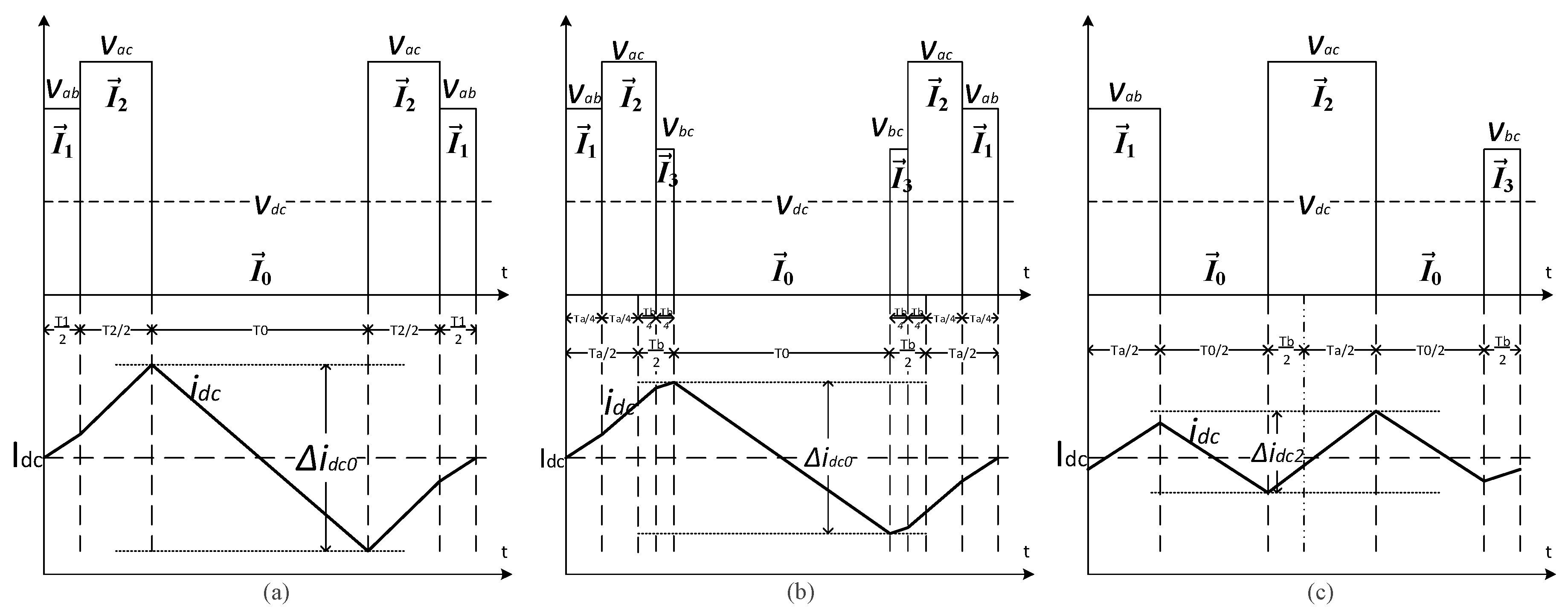
3.1. DC Current Ripple Analysis of C-SVM
3.2. DC Current Ripple Analysis of Proposed VSVM
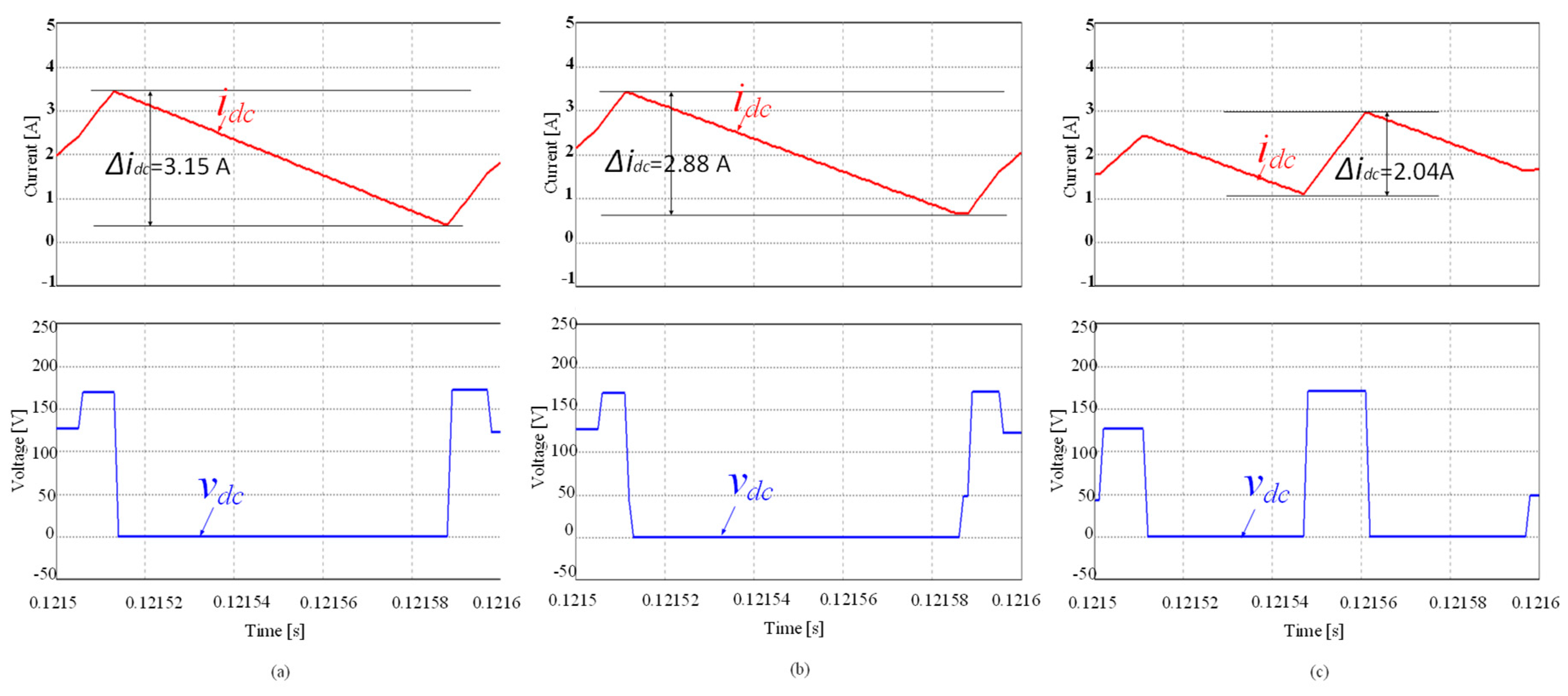
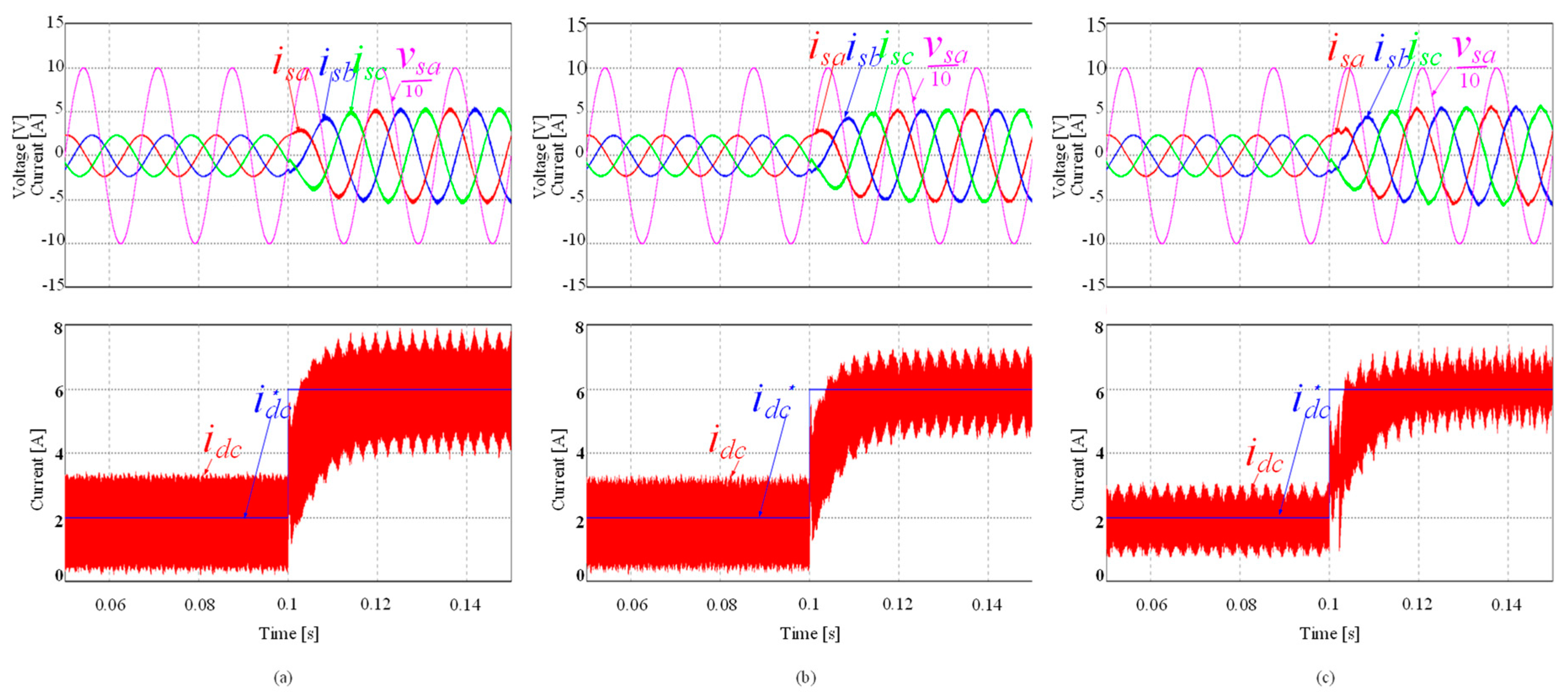
4. Simulation and Experimental Results
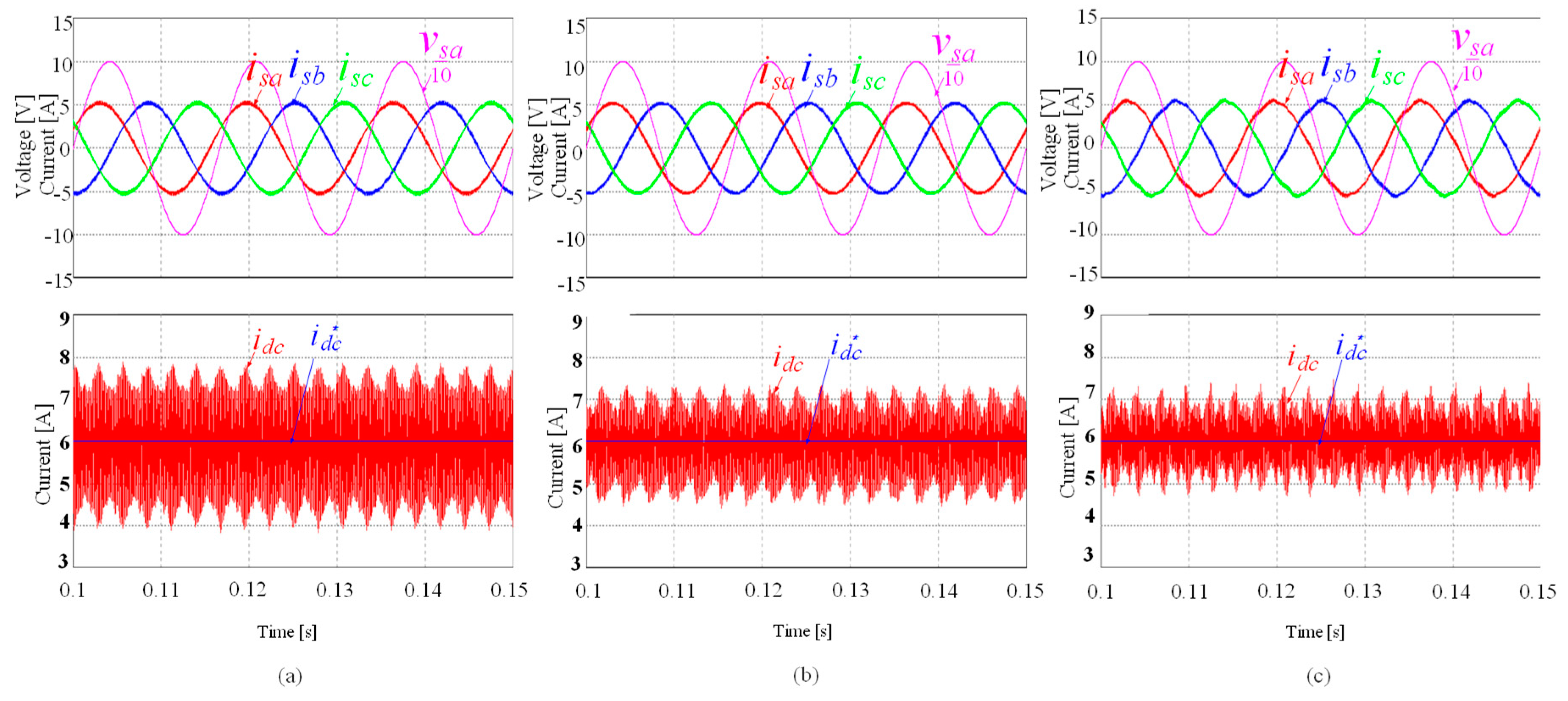
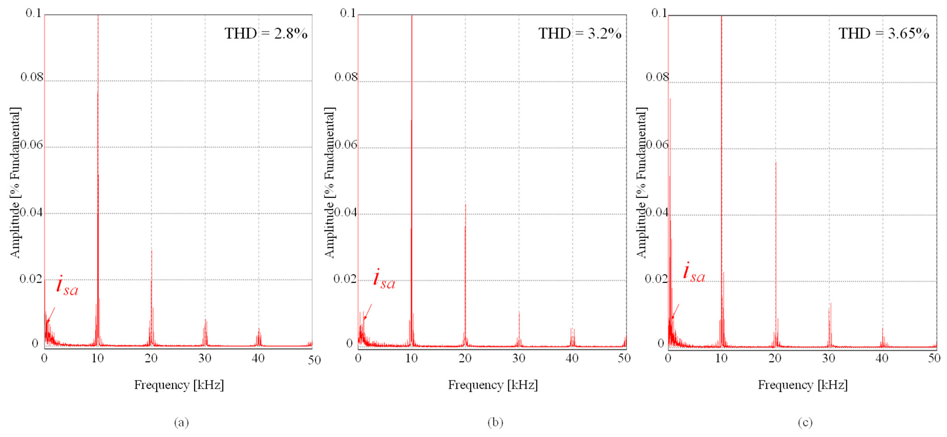
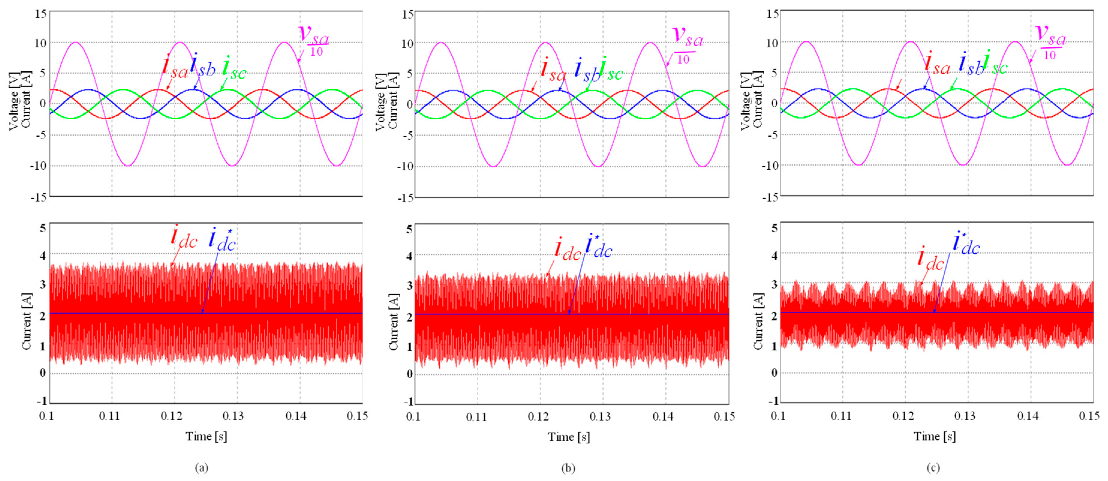
4.1. Simulation
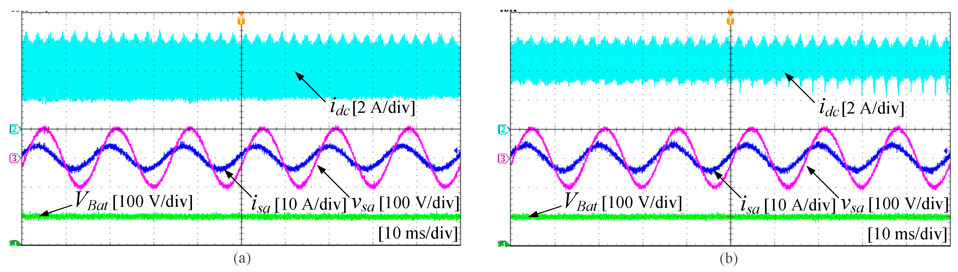
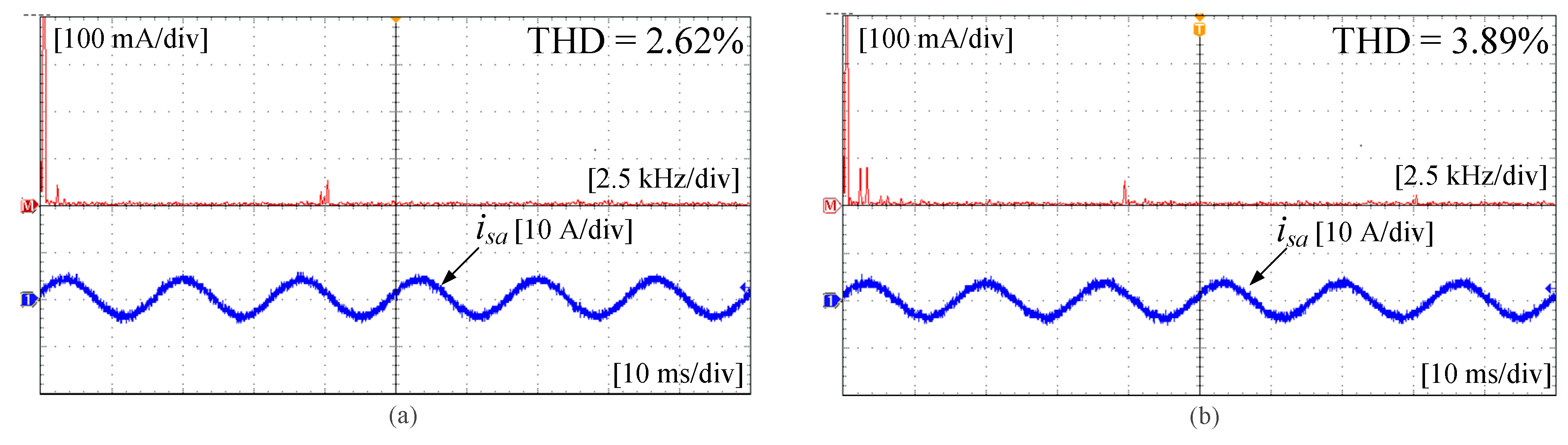
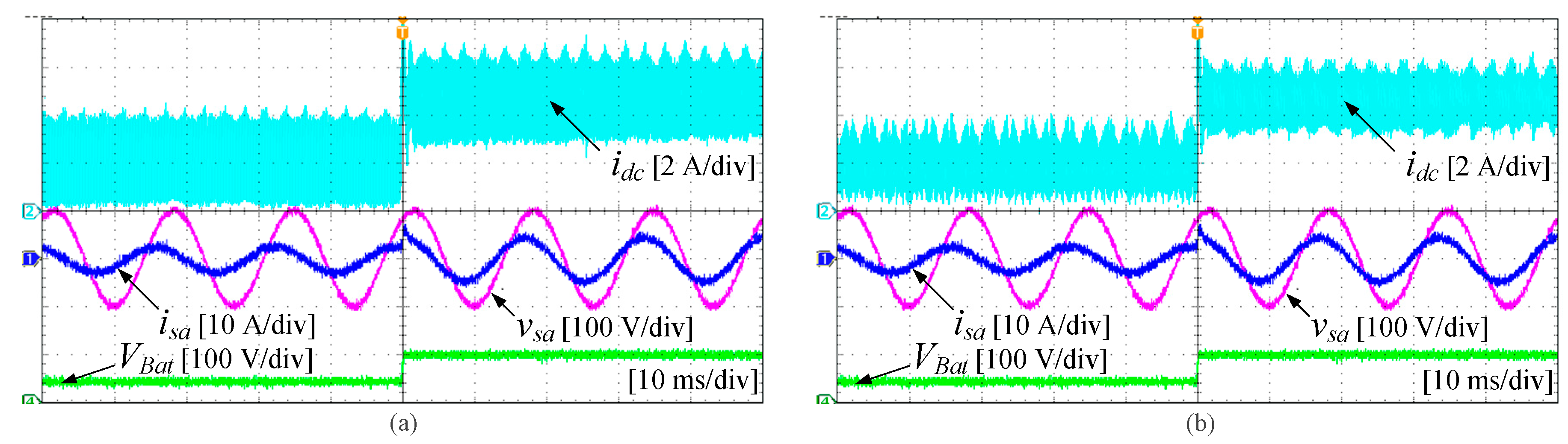
4.2. Experiment
5. Conclusions
Author Contributions
Funding
Acknowledgments
Conflicts of Interest
References
- Casadei, D.; Serra, G.; Tani, A.; Zari, L. Matrix converter modulation strategies: A new general approach based on space-vector representation of the switching state. IEEE Trans. Ind. Electron. 2002, 49, 370–381. [Google Scholar] [CrossRef]
- Nguyen, T.D.; Lee, H. Modulation Strategies to reduce common-mode voltage for indirect matrix converters. IEEE Trans. Ind. Electron. 2012, 59, 129–140. [Google Scholar] [CrossRef]
- Rivera, M.; Wilson, A.; Rojas, C.A.; Rodrigez, J.; Espinoza, J.R.; Wheeler, P.W.; Empringham, L. A comparative assessment of model predictive current control and space vector modulation in a direct matrix converter. IEEE Trans. Ind. Electron. 2013, 60, 578–588. [Google Scholar] [CrossRef]
- Rodriguez, J.; Rivera, M.; Kolar, J.W.; Wheeler, P.W. A review of control and modulation methods for matrix converters. IEEE Trans. Ind. Electron. 2012, 59, 58–70. [Google Scholar] [CrossRef]
- Alesina, A.; Venturini, M.G.B. Analysis and design of optimim-amplitude nine-switch direct AC-AC converter. IEEE Trans. Power. Electron. 1989, 4, 101–112. [Google Scholar] [CrossRef]
- Vazquez, S.; Lukic, S.M.; Galvan, E.; Franquelo, L.G.; Carrasco, J.M. Energy storage systems for transport and grid applications. IEEE Trans. Ind. Electron. 2010, 57, 3881–3895. [Google Scholar] [CrossRef]
- Yilmaz, M.; Krein, P. Review of battery charger topologies, charging power levels and infrastructure for plug-in electric and hybrid vehicles. IEEE Trans. Power Electron. 2013, 28, 2151–2169. [Google Scholar] [CrossRef]
- Bhuiyan, F.A.; Yazdani, A. Energy storage technologies for grid connected and off-grid power system applications. In Proceedings of the 2012 IEEE Electrical Power and Energy Conference (EPEC), London, ON, Canada, 10–12 October 2012; pp. 303–310. [Google Scholar]
- Roberts, B.P.; Sandberg, C. The role of energy storage in development of smart grids. Proc. IEEE 2011, 99, 1139–1144. [Google Scholar] [CrossRef]
- Loh, P.C.; Rong, R.; Blaabjerg, F.; Wang, P. Digital carrier modulation and sampling issues of matrix converters. IEEE Trans. Power Electron. 2009, 24, 1690–1700. [Google Scholar] [CrossRef]
- Yan, Z.; Jia, M.; Zhang, C.; Wu, W. An integration SPWM strategy for high-frequency link matrix converter with adaptive commutation in one step based on De-Re-coupling idea. IEEE Trans. Power Electron. 2012, 59, 116–128. [Google Scholar] [CrossRef]
- Nguyen, T.; Lee, H. An enhanced control strategy for ac/dc matrix converters under unbalanced grid voltage. IEEE Trans. Ind. Electron. 2019, 1718–1727. [Google Scholar] [CrossRef]
- Nguyen, T.; Lee, H. Simplified model predictive control for ac/dc matrix converters with active damping function under unbalanced grid voltage. IEEE J. Emerg. Sel. Top. Power Electron. 2019. [Google Scholar] [CrossRef]
- Gokdag, M.; Gulbudak, O. Model predictive control of ac-dc matrix converter with unity input power factor. In Proceedings of the IEEE 12th International Conference on Compatibility Power Electronics and Power Engineering (CPE-POWERENG 2018), Doha, Qatar, 10–12 April 2018. [Google Scholar]
- Metidji, R.; Metidji, B.; Mendil, B. Design and implementation of unity power factor fuzzy battery charger using ultrasparse matrix rectifier. IEEE Trans. Power Electron. 2013, 28, 2269–2276. [Google Scholar] [CrossRef]
- You, K.; Xiao, D.; Rahman, M.F.; Uddin, M.N. Applying reduced general direct space vector modulation approach of AC-AC matrix converter theory to achieve direct power factor controlled three-phase AC-DC matrix rectifier. IEEE Trans. Ind. Electron. 2014, 50, 2243–2257. [Google Scholar] [CrossRef]
- Feng, B.; Lin, H.; Wang, X. Modulation and control of ac/dc matrix converter for battery energy storage application. IET Power Electron. 2015, 8, 1583–1594. [Google Scholar] [CrossRef]
- Feng, B.; Lin, H.; Hu, S.; An, X.; Wang, X. Control strategy of AC-DC matrix converter in battery energy storage system. In Proceedings of the IEEE Energy Conversion Congress and Exposition (ECCE), Raleigh, NC, USA, 15–20 September 2012; pp. 2128–2134. [Google Scholar]
- Feng, B.; Lin, H.; Wang, X.; An, X.; Liu, B. Optimal zero-vector configuration for space vector modulated AC-DC matrix converter. In Proceedings of the IEEE Energy Conversion Congress and Exposition (ECCE), Raleigh, NC, USA, 15–20 September 2012; pp. 291–297. [Google Scholar]
- Su, M.; Wang, H.; Sun, Y.; Yang, J.; Xiong, W.; Liu, Y. AC/DC matrix converter with an optimized modulation strategy for V2G applications. IEEE Trans. Power Electron. 2013, 28, 5736–5745. [Google Scholar] [CrossRef]
- Kim, J.; Kwak, S.; Kim, T. Power factor control method based on virtual capacitor for three-phase matrix rectifiers. IEEE Access 2019, 7, 12484–12494. [Google Scholar] [CrossRef]
- Holmes, D.G.; Lipo, T.A. Implementation of a controlled rectifier using AC–AC matrix converter theory. IEEE Trans. Power Electron. 1992, 7, 240–250. [Google Scholar] [CrossRef]
- Ratanapanachote, S.; Cha, H.J.; Enjeti, P.N. A digitally controlled switch mode power supply based on matrix converter. IEEE Trans. Power Electron. 2006, 21, 124–130. [Google Scholar] [CrossRef]
- Yang, X.J.; Cai, W.; Ye, P.S.; Gong, Y.M. Research on dynamic characteristics of matrix rectifier. In Proceedings of the IEEE Conference on Industrial Electronics and Applications, Singapore, 24–26 May 2006; pp. 1–6. [Google Scholar]
- Guo, X.; Yang, Y.; Wang, X. Optimal space vector modulation of current source converter for DC link current ripple reduction. IEEE Trans. Ind. Electron. 2019, 66, 1671–1680. [Google Scholar] [CrossRef]
- Tian, K.; Wang, J.; Wu, B.; Xu, D.; Cheng, Z.; Zargari, N.R. A virtual space vector modulation technique for the reduction of common-mode voltage in both magnitude and third-order component. IEEE Trans. Power Electron. 2016, 31, 839–848. [Google Scholar] [CrossRef]
- Hu, C.; Yu, X.; Holmes, D.G.; Shen, W.; Wang, Q.; Luo, F.; Liu, N. An improved virtual space vector modulation scheme for three-level active neutral-point-clamped inverter. IEEE Trans. Power Electron. 2017, 32, 7419–7434. [Google Scholar] [CrossRef]
- Gang, L.; Dafang, W.; Miaoran, W.; Cheng, Z.; Mingyu, W. Neutral-point-voltage balancing in three-level inverters using an optimized virtual space vector PWM with reduced commutations. IEEE Trans. Ind. Electron. 2018, 65, 6959–6969. [Google Scholar]


| Parameters | Value |
|---|---|
| Source phase voltage () | 100 V |
| Source frequency () | 60 Hz |
| Input filter inductance () | 2.5 mH |
| Input filter capacitance () | 60 µF |
| Output filter inductance () | 1 mH |
| Output filter capacitance () | 40 µF |
| Load resistance () | 20 Ω |
| Sampling frequency () | 10 kHz |
| Compared by | Proposed VSVM Method | |
|---|---|---|
| Percentage of Reducing DC Current Ripple | Percentage of Increasing THD | |
| C-SVM | 43.1% | 30.36% |
| C-VSVM | 31.25% | 14.06% |
© 2019 by the authors. Licensee MDPI, Basel, Switzerland. This article is an open access article distributed under the terms and conditions of the Creative Commons Attribution (CC BY) license (http://creativecommons.org/licenses/by/4.0/).
Share and Cite
Dang, H.-L.; Jun, E.-S.; Kwak, S. Reduction of DC Current Ripples by Virtual Space Vector Modulation for Three-Phase AC–DC Matrix Converters. Energies 2019, 12, 4319. https://doi.org/10.3390/en12224319
Dang H-L, Jun E-S, Kwak S. Reduction of DC Current Ripples by Virtual Space Vector Modulation for Three-Phase AC–DC Matrix Converters. Energies. 2019; 12(22):4319. https://doi.org/10.3390/en12224319
Chicago/Turabian StyleDang, Hoang-Long, Eun-Su Jun, and Sangshin Kwak. 2019. "Reduction of DC Current Ripples by Virtual Space Vector Modulation for Three-Phase AC–DC Matrix Converters" Energies 12, no. 22: 4319. https://doi.org/10.3390/en12224319
APA StyleDang, H.-L., Jun, E.-S., & Kwak, S. (2019). Reduction of DC Current Ripples by Virtual Space Vector Modulation for Three-Phase AC–DC Matrix Converters. Energies, 12(22), 4319. https://doi.org/10.3390/en12224319