Passivity-Based Control Design Methodology for UPS Systems


Abstract
:1. Introduction
2. The Output Filter Parameters
3. Initial State Space Models of Three-Phase Inverters in the Stationary αβ and Rotating dq Frames
4. Three-Phase Voltage Source Inverter Controller Design
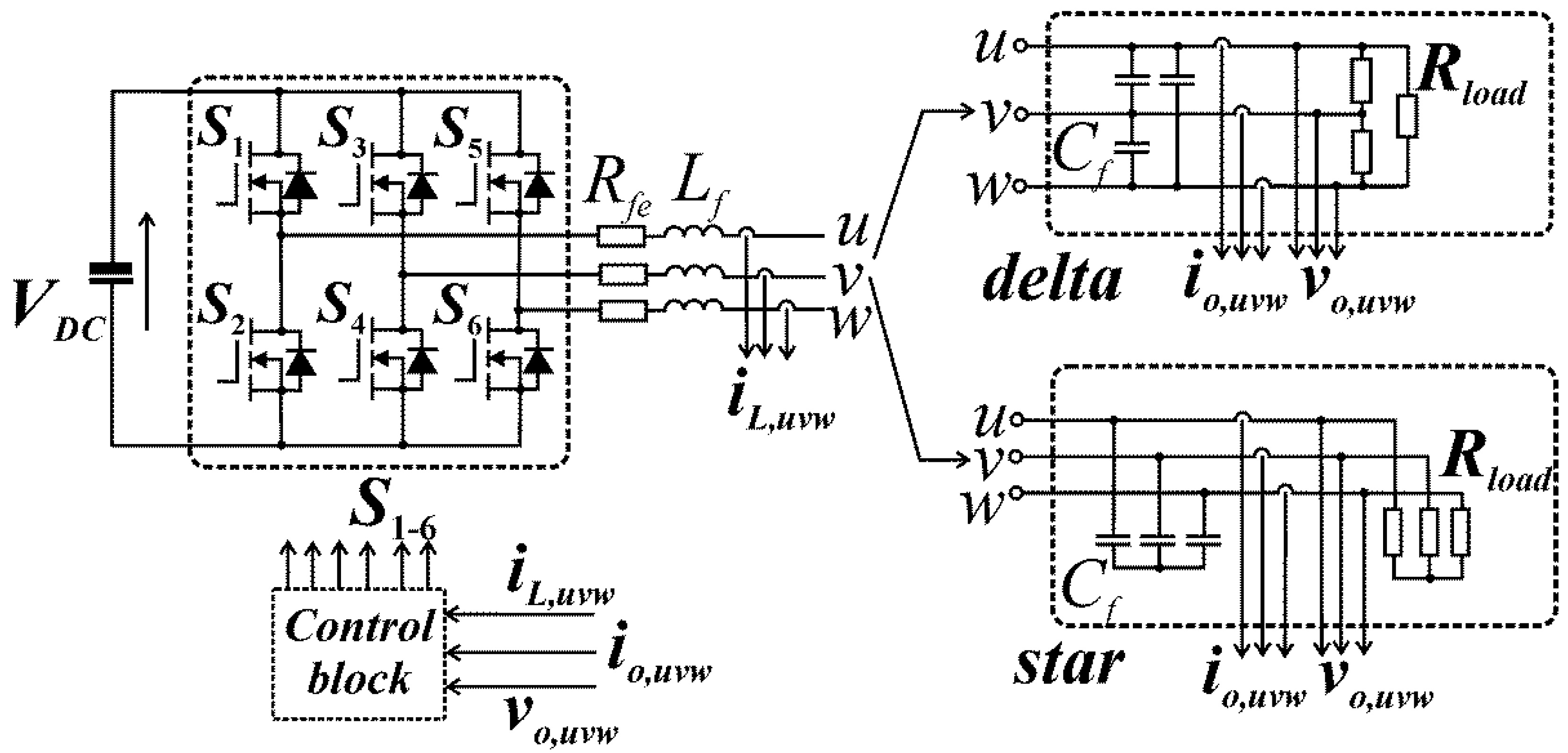
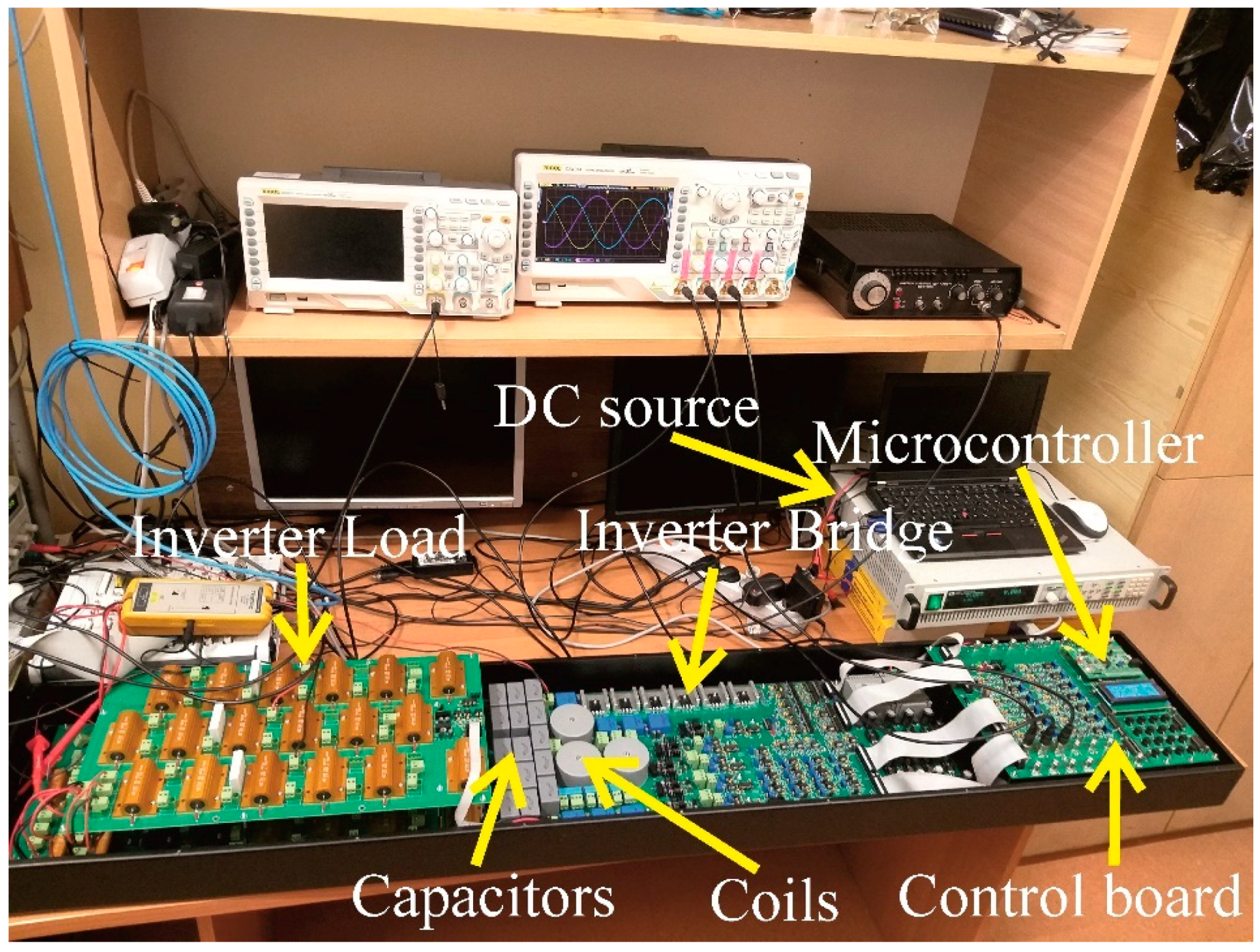
5. Modeling and Measurement of a Three-Phase Inverter with IPBC2 and IDA–PBC Control for Standard Loads
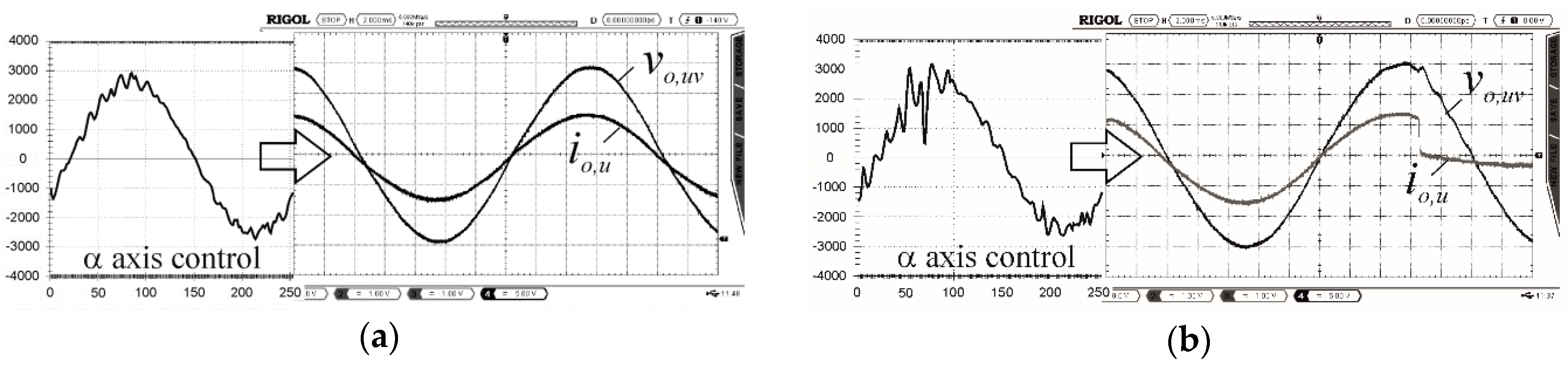
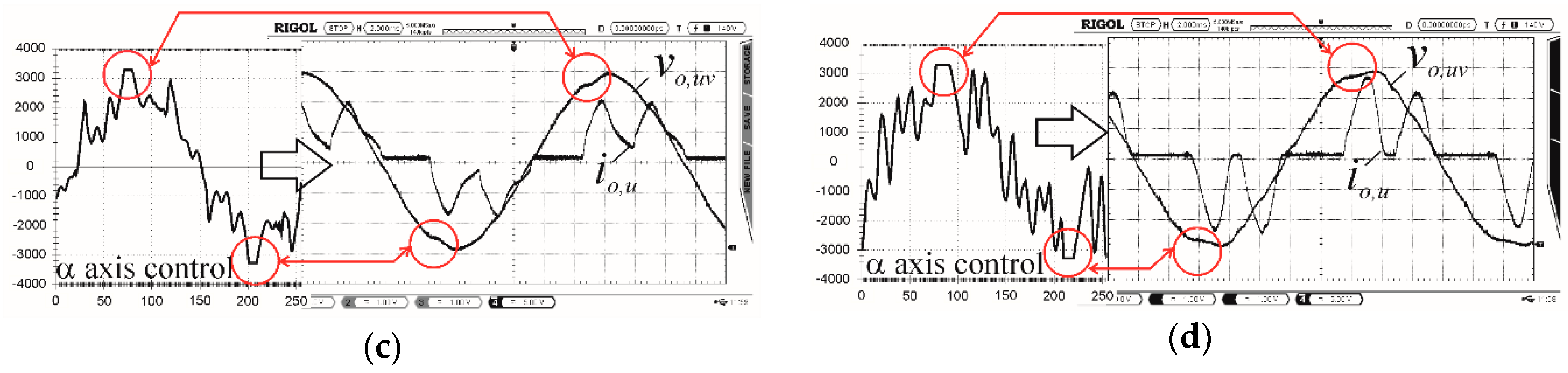
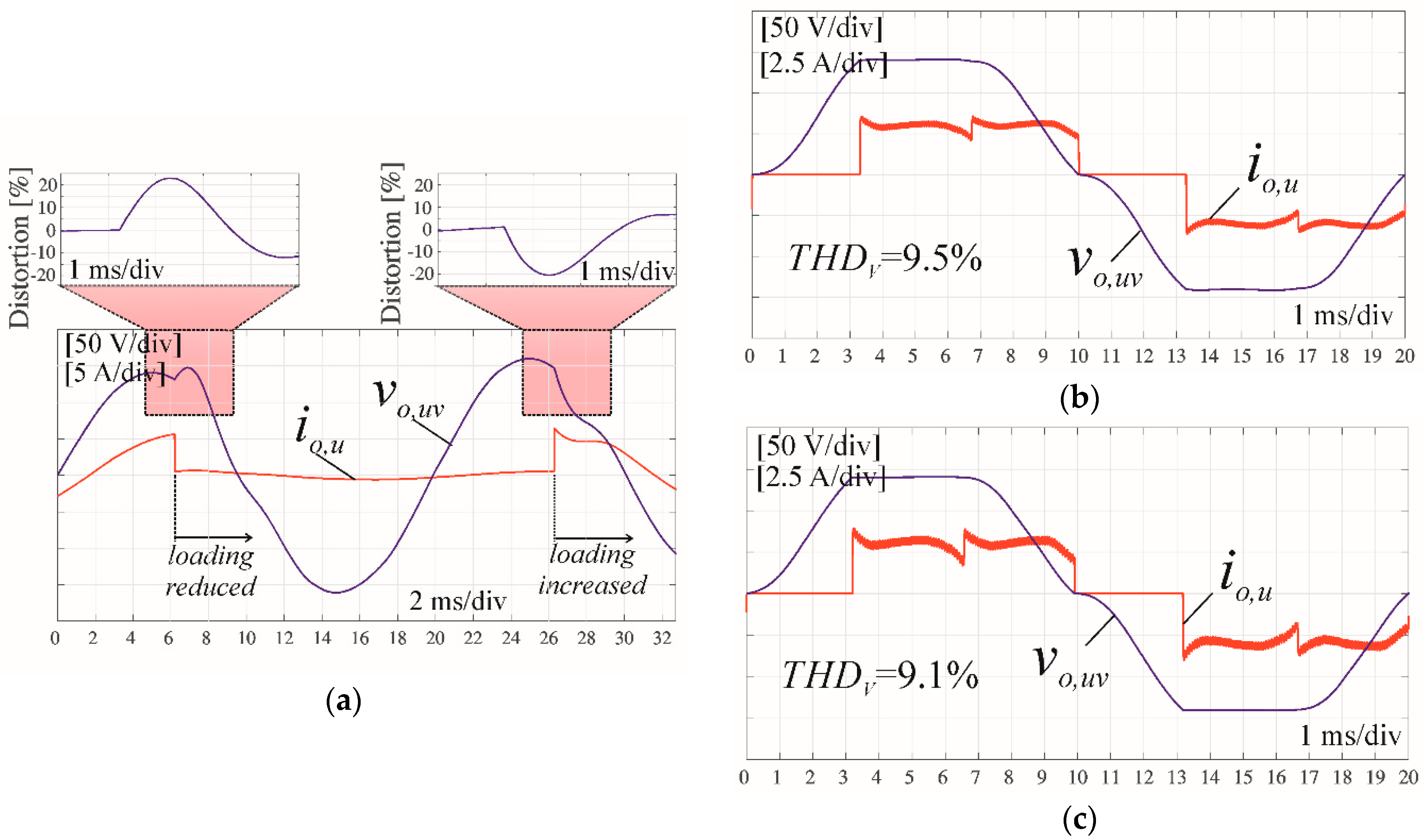
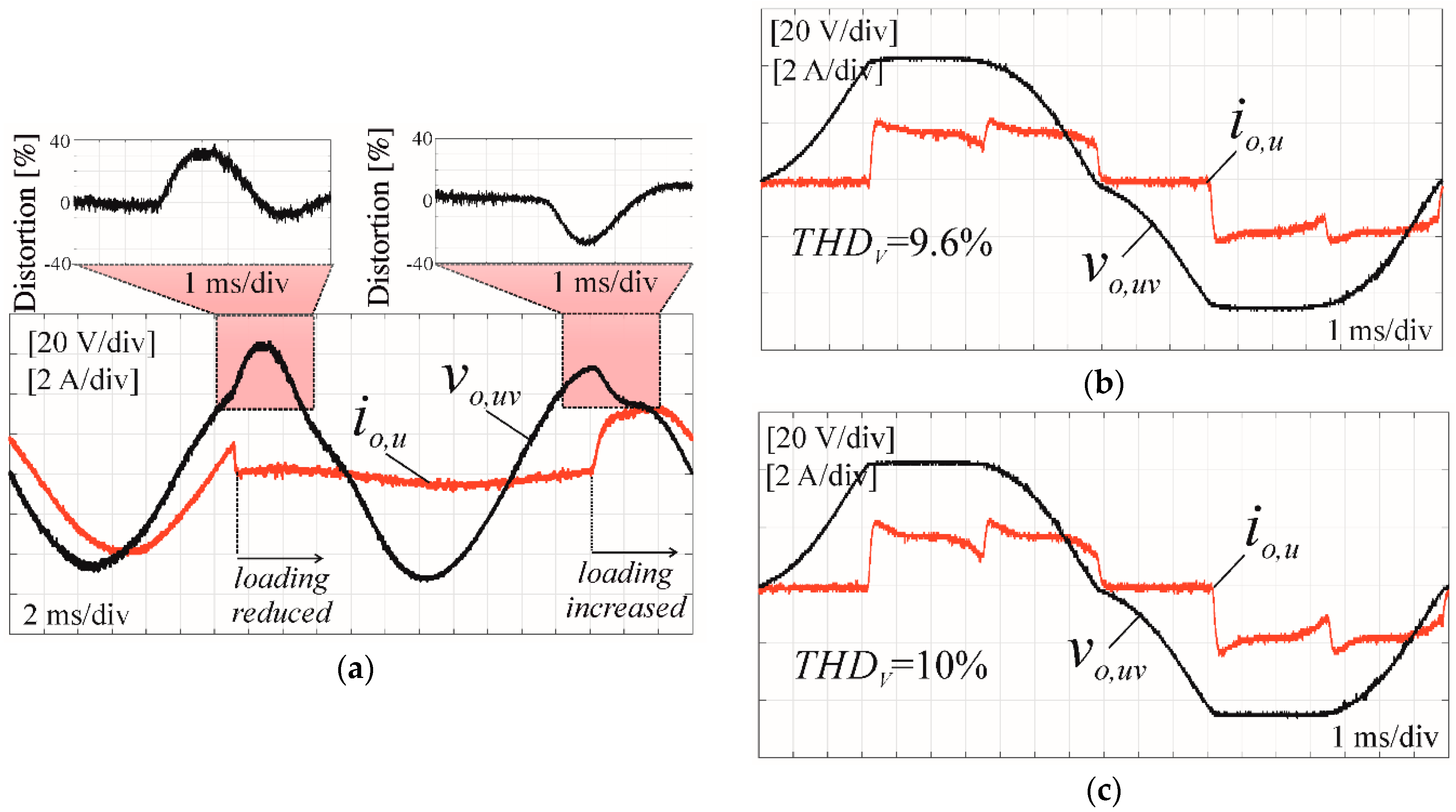
6. Results
6.1. Modulation Index Choice
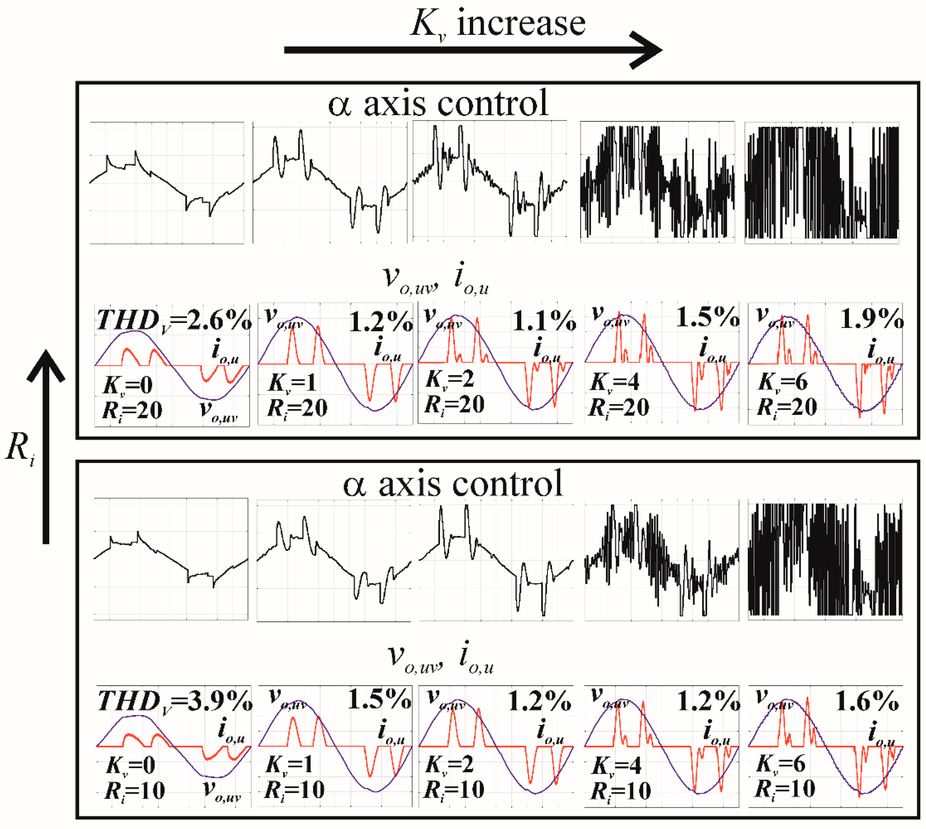
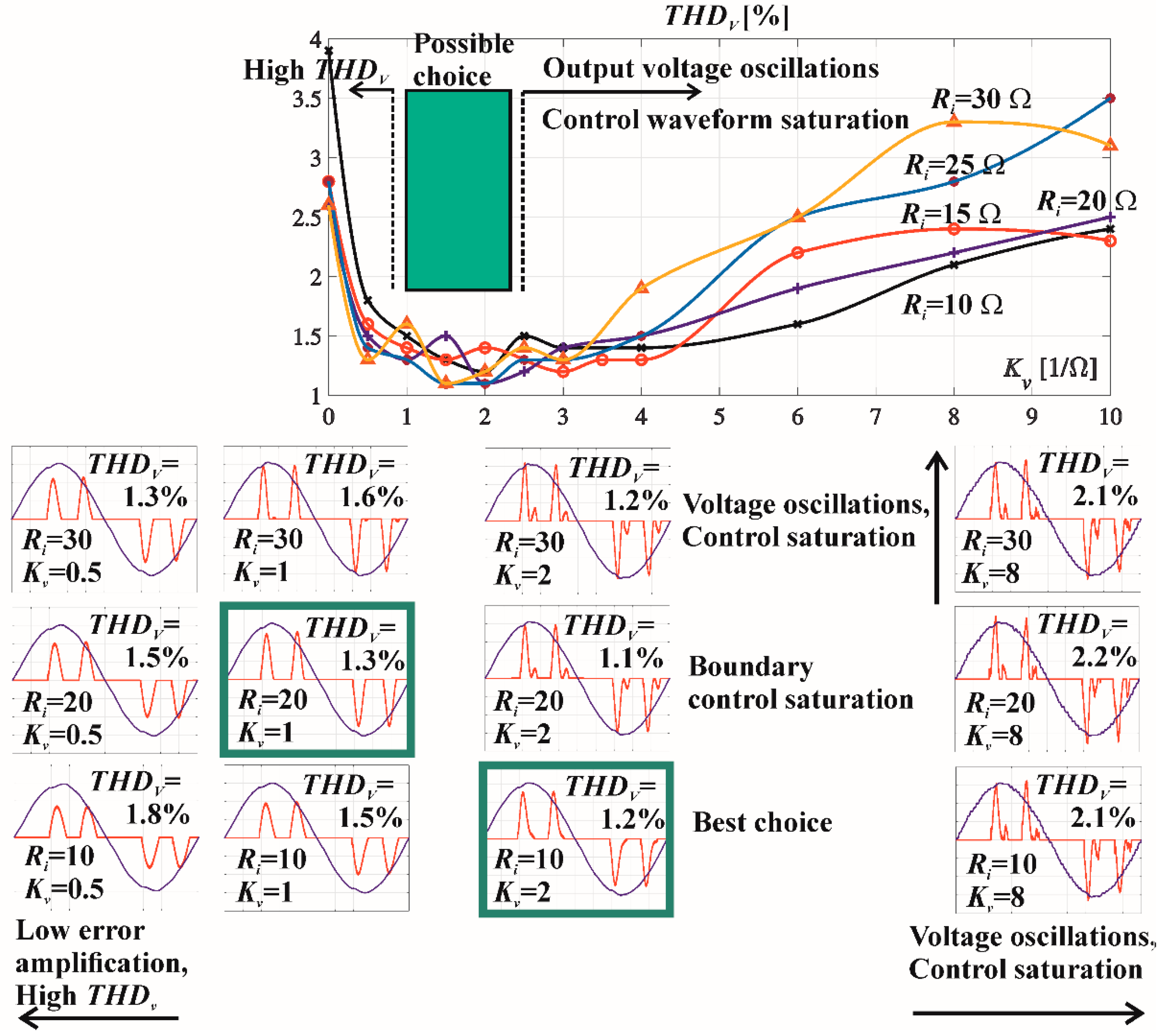
6.2. Controller Gains Adjustment
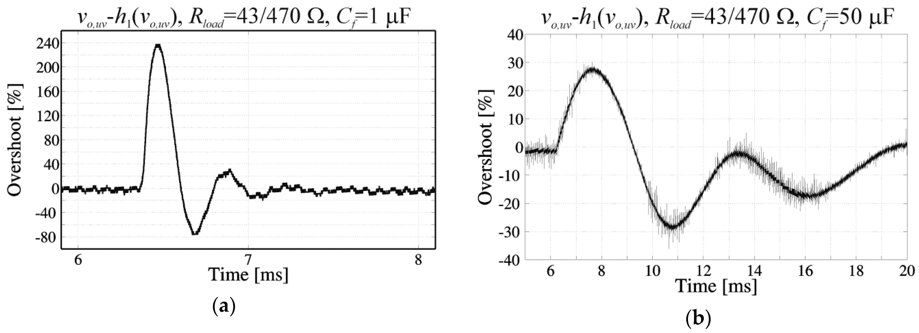
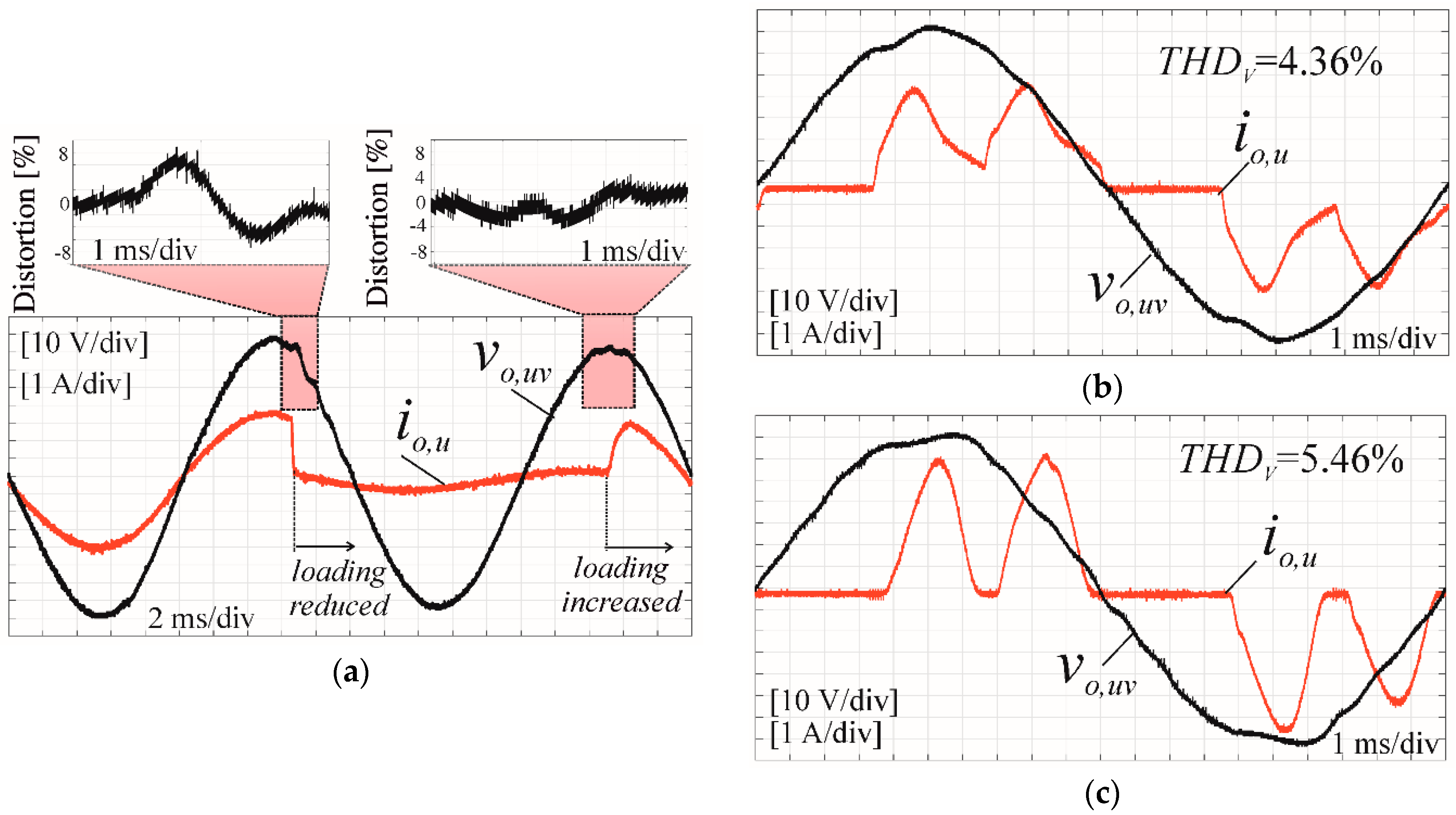
6.3. Differences Between Results of the Simulation and the Experimental Inverter Measurements
6.4. Advantages of the Control in the Stationary Frame
6.5. The Steady-State Error Reduction
7. Discussion
8. Conclusions
Author Contributions
Funding
Acknowledgments
Conflicts of Interest
References
- Ben-Brahim, L.; Yokoyama, T.; Kawamura, A. Digital control for UPS inverters. In Proceedings of the Fifth International Conference on Power Electronics and Drive Systems, Singapore, 17–20 November 2003; pp. 1252–1257. [Google Scholar]
- Kawamura, A.; Yokoyama, T. Comparison of five different approaches for real time digital feedback control of PWM inverters. In Proceedings of the IEEE Industry Applied Society Annual Meeting, Seattle, WA, USA, 7–12 October 1990; pp. 1005–1011. [Google Scholar]
- Luo, F.L.; Ye, H.; Rashid, M. Digital Power Electronics and Applications; Elsevier Academic Press: San Diego, CA, USA, 2010. [Google Scholar]
- Rech, C.; Pinheiro, H.; Grundling, H.A.; Hey, H.L.; Pinheiro, J.R. Comparison of Digital Control Techniques with Repetitive Integral Action for Low Cost PWM Inverters. IEEE Trans. Power Electron. 2003, 18, 401–410. [Google Scholar] [CrossRef]
- Sangwongwanich, A.; Abdelhakim, A.; Yangand, Y.; Zhou, K. Control of Single-Phase and Three-Phase DC/AC Converters. In Control of Power Electronic Converters and Systems; Blaabjerg, F., Ed.; Elsevier Academic Press: London, UK, 2018; Volume 6, pp. 153–172. [Google Scholar]
- Zou, Z.X.; Wang, Z.; Cheng, M. Design and analysis of operating strategies for a generalised voltage-source power supply based on internal model principle. IET Power Electron. 2014, 7, 330–339. [Google Scholar] [CrossRef]
- Gui, Y.; Wei, B.; Li, M.; Guerrero, J.M.; Vasquez, J.C. Passivity-based coordinated control for islanded AC microgrid. Appl. Energy 2018, 229, 551–561. [Google Scholar] [CrossRef]
- Uninterruptible Power Systems (UPS)—Part 3: Method of Specifying the Performance and Test Requirements. Available online: https://webstore.iec.ch/publication/6344 (accessed on 10 October 2019).
- Blachuta, M.; Rymarski, Z.; Bieda, R.; Bernacki, K.; Grygiel, R. Design, Modeling and Simulation of PID Control for DC/AC Inverters. In Proceedings of the 24th International Conference on Methods and Models in Automation and Robotics, Międzyzdroje, Poland, 26–29 August 2019; pp. 428–433. [Google Scholar]
- Manabe, S. Importance of coefficient diagram in polynomial method. In Proceedings of the 42nd IEEE Conference on Decision and Control, Maui, HI, USA, 9–12 December 2003; pp. 3489–3494. [Google Scholar]
- Zhao, G.; Miao, G.; Yong, W. Application of Repetitive Control for Aeronautical Static Inverter. In Proceedings of the 2nd IEEE Conference on Industrial Electronics and Applications, Harbin, China, 23–25 May 2007; pp. 121–125. [Google Scholar]
- Rymarski, Z. Design method of single-phase inverters for UPS systems. Int. J. Electron. 2009, 96, 521–535. [Google Scholar] [CrossRef]
- Ortega, R.; Spong, M.W. Adaptive motion control of rigid robots: A tutorial. Automatica 1989, 25, 877–888. [Google Scholar] [CrossRef]
- Ortega, R.; Perez, J.A.L.; Nicklasson, P.J.; Sira-Ramirez, H.J.; Sira-Ramirez, H. Passivity-Based Control of Euler-Lagrange Systems: Mechanical, Electrical and Electromechanical Applications (Communications and Control Engineering); Springer: London, UK, 1998. [Google Scholar]
- Ortega, R.; Garcia-Canseco, E. Interconnection and Damping Assignment Passivity-Based Control: A Survey. Eur. J. Control 2004, 5, 432–450. [Google Scholar] [CrossRef]
- Ortega, R.; Garcia-Canseco, E. Interconnection and Damping Assignment Passivity-Based Control: Towards a Constructive Procedure—Part I. In Proceedings of the 43rd IEEE Conference on Decision and Control, Nassau, Bahamas, 14–17 December 2004; pp. 3412–3417. [Google Scholar]
- Ortega, R.; Espinosa-Perez, G. Passivity-based control with simultaneous energy-shaping and damping injection: The induction motor case study. IFAC Proc. Vol. 2005, 38, 477–482. [Google Scholar] [CrossRef]
- Torres, M.; Ortega, R. Feedback Linearization, Integrator Backstepping and Passivity-Based Controller Designs: A Comparison Example. In Perspectives in Control. Theory and Applications; Normand-Cyrot, D., Ed.; Springer: London, UK, 1998. [Google Scholar]
- Wang, W.J.; Chen, J.Y. Compositive adaptive position control of induction motors based on passivity theory. IEEE Trans. Energy Convers. 2001, 16, 180–185. [Google Scholar] [CrossRef]
- Wang, W.J.; Chen, J.Y. Passivity-based sliding mode position control for induction motor drives. IEEE Trans. Energy Convers. 2005, 20, 316–321. [Google Scholar] [CrossRef]
- Hill, D.; Zhao, J.; Gregg, R.; Ortega, R. 20 Years of Passivity-Based Control (PBC): Theory and Applications. In Proceedings of the CDC Workshop, Shanghai, China, 15 December 2009; pp. 1–85. [Google Scholar]
- Komurcugil, H. Improved passivity-based control method and its robustness analysis for single-phase uninterruptible power supply inverters. IET Power Electron. 2015, 8, 1558–1570. [Google Scholar] [CrossRef]
- Jie, B.; Lee, P.L. Passivity-based Robust Control. In Advances in Industrial Control; Springer: London, UK, 2007; pp. 43–88. [Google Scholar]
- Bu, N.; Deng, M.C. Passivity-based robust control for uncertain nonlinear feedback systems. J. Robot. Mechatron. 2016, 28, 837–841. [Google Scholar] [CrossRef]
- Rymarski, Z.; Bernacki, K.; Dyga, Ł. A control for an unbalanced 3-phase load in UPS systems. Elektronika Ir Elektrotechnika 2018, 24, 27–31. [Google Scholar] [CrossRef]
- Available online: https://iris.unicampania.it/handle/11591/178750#.XcZk89URXIV (accessed on 10 October 2019).
- Serra, F.M.; De Angelo, C.H.; Forchetti, D.G. IDA-PBC control of a DC-AC converter for sinusoidal three-phase voltage generation. Int. J. Electron. 2017, 104, 93–110. [Google Scholar] [CrossRef]
- Khefifi, N.; Houari, A.; Ait-Ahmed, M.; Machmoum, M.; Ghanes, M. Robust IDA-PBC based Load Voltage Controller for Power Quality Enhancement of Standalone Microgrids. In Proceedings of the IEEE IECON 2018—44th Annual Conference of the IEEE Industrial Electronics Society, Washington, DC, USA, 21–23 October 2018; pp. 249–254. [Google Scholar]
- Meshram, R.V.; Bhagwat, M.; Khade, S.; Wagh, S.R.; Aleksandar, M.; Stankovic, A.M.; Singh, N.M. Port-Controlled Phasor Hamiltonian Modeling and IDA-PBC Control of Solid-State Transformer. IEEE Trans. Control Syst. Technol. 2019, 27, 161–174. [Google Scholar] [CrossRef]
- Dahono, P.A.; Purwadi, A.; Qamaruzzaman. An LC filter design method for single-phase PWM inverters. In Proceedings of the International Conference on Power Electronics and Drive System, Singapore, 21–24 February 1995; pp. 571–576. [Google Scholar]
- Rymarski, Z. The discrete model of power stage of the voltage source inverter for UPS. Int. J. Electron. 2001, 98, 1291–1304. [Google Scholar] [CrossRef]
- Rymarski, Z. The analysis of output voltage distortion minimization in the 3-phase VSI for the nonlinear rectifier ROCO load. Przegląd Elektrotechniczny (Electr. Rev.) 2009, 85, 127–132. [Google Scholar]
- Chattopadhyay, S.; Mitra, M.; Sengupta, S. Electric Power Quality; Springer: Dordrecht, The Netherlands, 2013. [Google Scholar]
- Akagi, H.; Watanabe, E.H.; Aredes, M. Instanteneous Power Theory and Application to Power Conditionig, In IEEE Press Series on Power Engineering; Willey-Interscience, Willey and Sons, Inc.: Hoboken, NJ, USA, 2007. [Google Scholar]
- Wang, Z.; Goldsmith, P. Modified energy-balancing-based control for the tracking problem. IET Control Theory Appl. 2008, 2, 310–312. [Google Scholar] [CrossRef]
- Rymarski, Z. Measuring the real parameters of single-phase voltage source inverters for UPS systems. Int. J. Electron. 2017, 104, 1020–1033. [Google Scholar] [CrossRef]
- 2019 Iron Powder Products Catalog. Available online: https://micrometals.com (accessed on 24 September 2019).
- Bernacki, K.; Rymarski, Z.; Dyga, Ł. Selecting the coil core powder material for the output filter of a voltage source inverter. IET Electron. 2017, 53, 1068–1069. [Google Scholar] [CrossRef]
- Rymarski, Z.; Bernacki, K.; Dyga, Ł. Decreasing the single phase inverter output voltage distortions caused by impedance networks. IEEE Trans. Ind. Appl. 2019. [Google Scholar] [CrossRef]


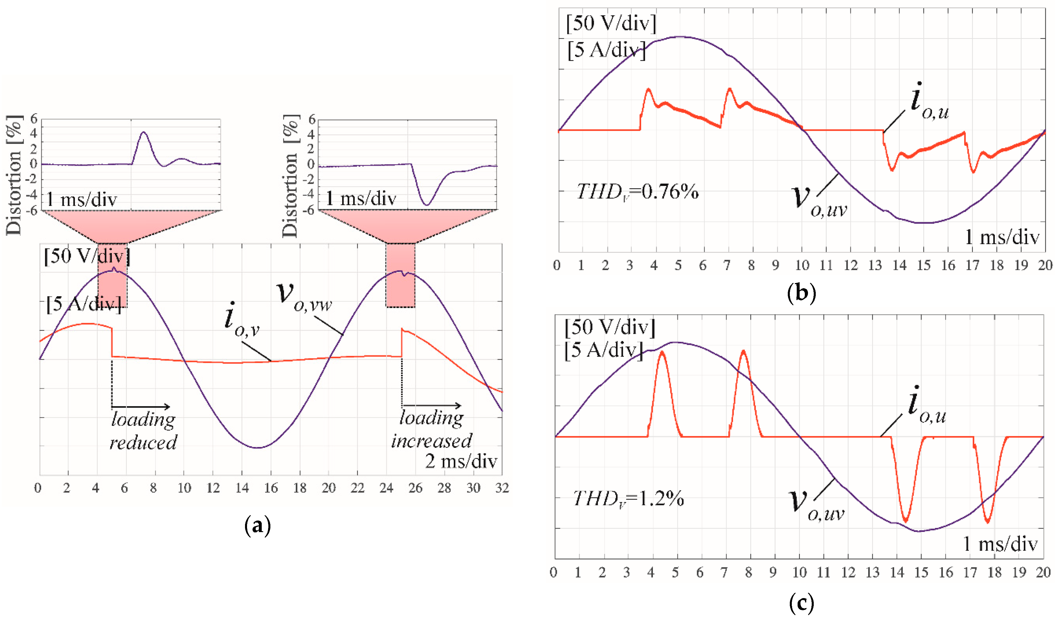
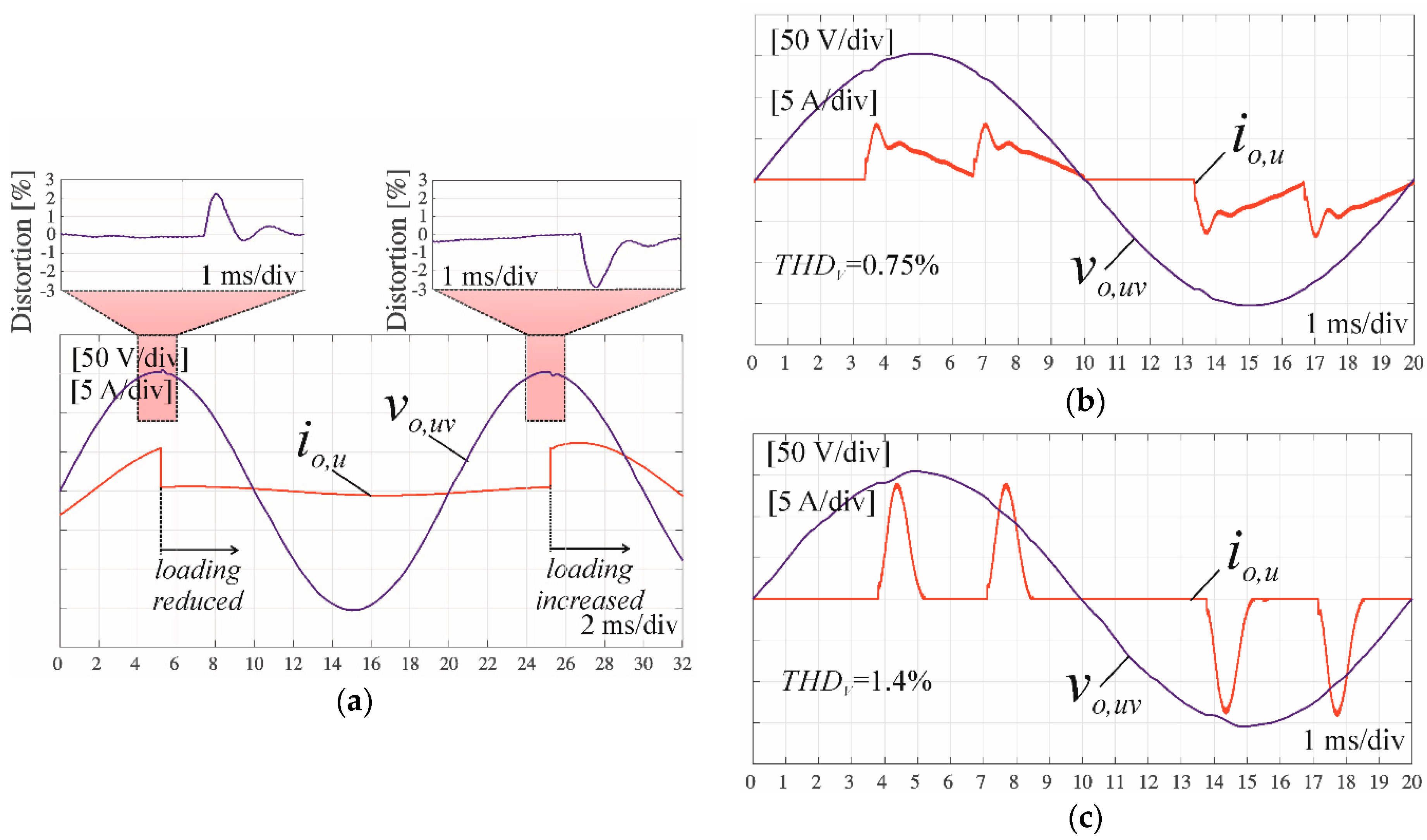
| Type of the Model | Lf (mH) | Rfe (Ω) | Cf (µF) | M | Vo,uv|max (V) | Ri (Ω) | Kv (Ω−1) |
|---|---|---|---|---|---|---|---|
| MATLAB Simulation | 3 | 1 | 50 | 0.3 | 150 | 10 | 2 |
| Experimental IPBC2 | 3 | 1 | 50 | 0.3 | 70 | 15 | 0.8 |
| Experimental IDA–PBC | 3 | 1 | 50 | 0.3 | 70 | 18 | 0.5 |
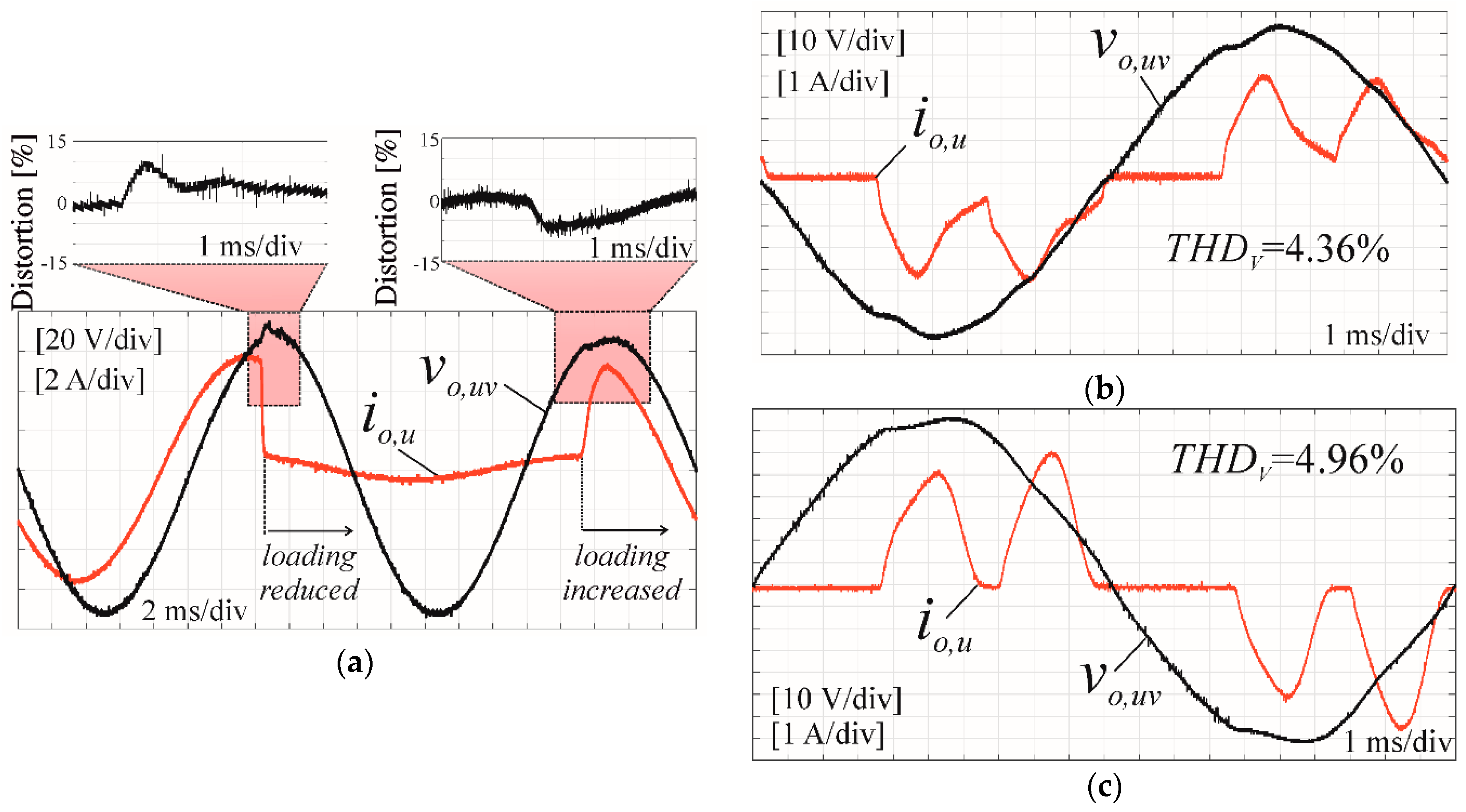
| Ri (Ω) | Kv (Ω−1) | THDV RC1 | THDV RC2 | Overshoot Load Decrease | Undershoot Load Increase | |
|---|---|---|---|---|---|---|
| No feedback. simulation | --- | --- | 9.5% | 9.1% | +23% | −20% |
| No feedback inverter | --- | --- | 9.6% | 10% | +32% | −28% |
| IPBC2 simulation | 10 | 2 | 0.76% | 1.2% | +4.5% | −5.5% |
| IPBC2 inverter | 15 | 0.8 | 4.36% | 5.46% | +7% | −4% |
| IDA–PBC simulation | 10 | 2 | 0.75% | 1.4% | +2.2% | −3% |
| IDA–PBC inverter | 18 | 0.5 | 3.93% | 4.96% | +10% | −7% |
© 2019 by the authors. Licensee MDPI, Basel, Switzerland. This article is an open access article distributed under the terms and conditions of the Creative Commons Attribution (CC BY) license (http://creativecommons.org/licenses/by/4.0/).
Share and Cite
Rymarski, Z.; Bernacki, K.; Dyga, Ł.; Davari, P. Passivity-Based Control Design Methodology for UPS Systems. Energies 2019, 12, 4301. https://doi.org/10.3390/en12224301
Rymarski Z, Bernacki K, Dyga Ł, Davari P. Passivity-Based Control Design Methodology for UPS Systems. Energies. 2019; 12(22):4301. https://doi.org/10.3390/en12224301
Chicago/Turabian StyleRymarski, Zbigniew, Krzysztof Bernacki, Łukasz Dyga, and Pooya Davari. 2019. "Passivity-Based Control Design Methodology for UPS Systems" Energies 12, no. 22: 4301. https://doi.org/10.3390/en12224301
APA StyleRymarski, Z., Bernacki, K., Dyga, Ł., & Davari, P. (2019). Passivity-Based Control Design Methodology for UPS Systems. Energies, 12(22), 4301. https://doi.org/10.3390/en12224301