A New Buck-Boost AC/DC Converter with Two-Terminal Output Voltage for DC Nano-Grid


Abstract
:1. Introduction
2. Proposed AC to DC Converter
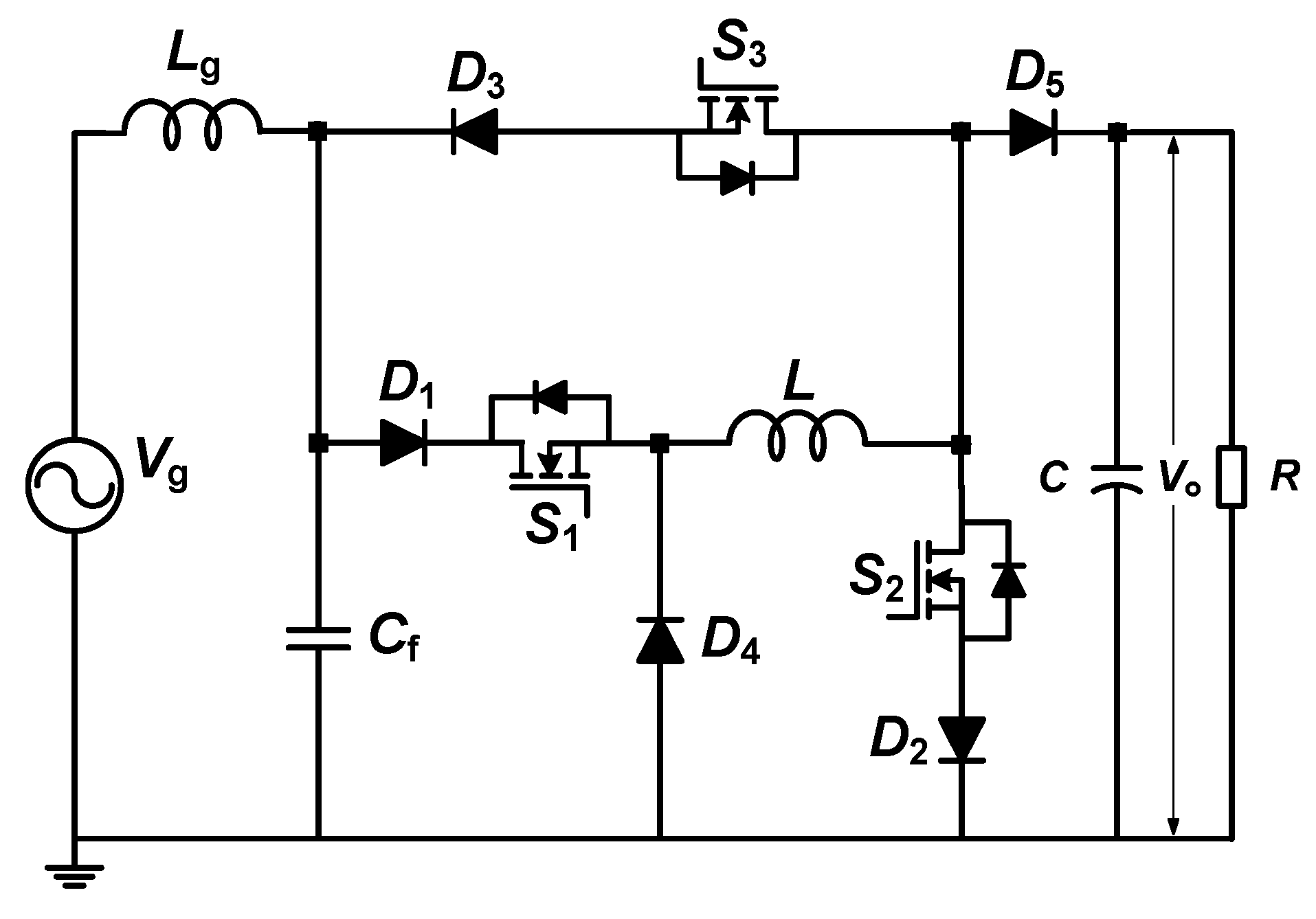
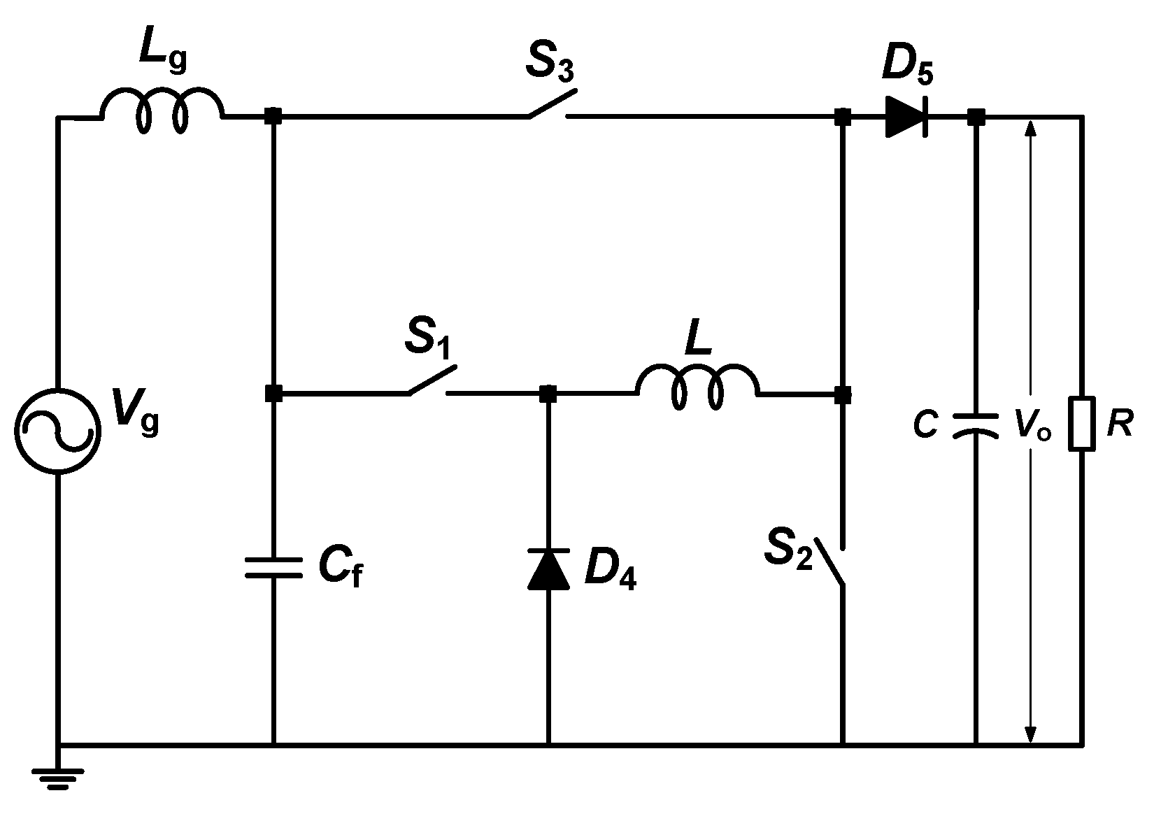
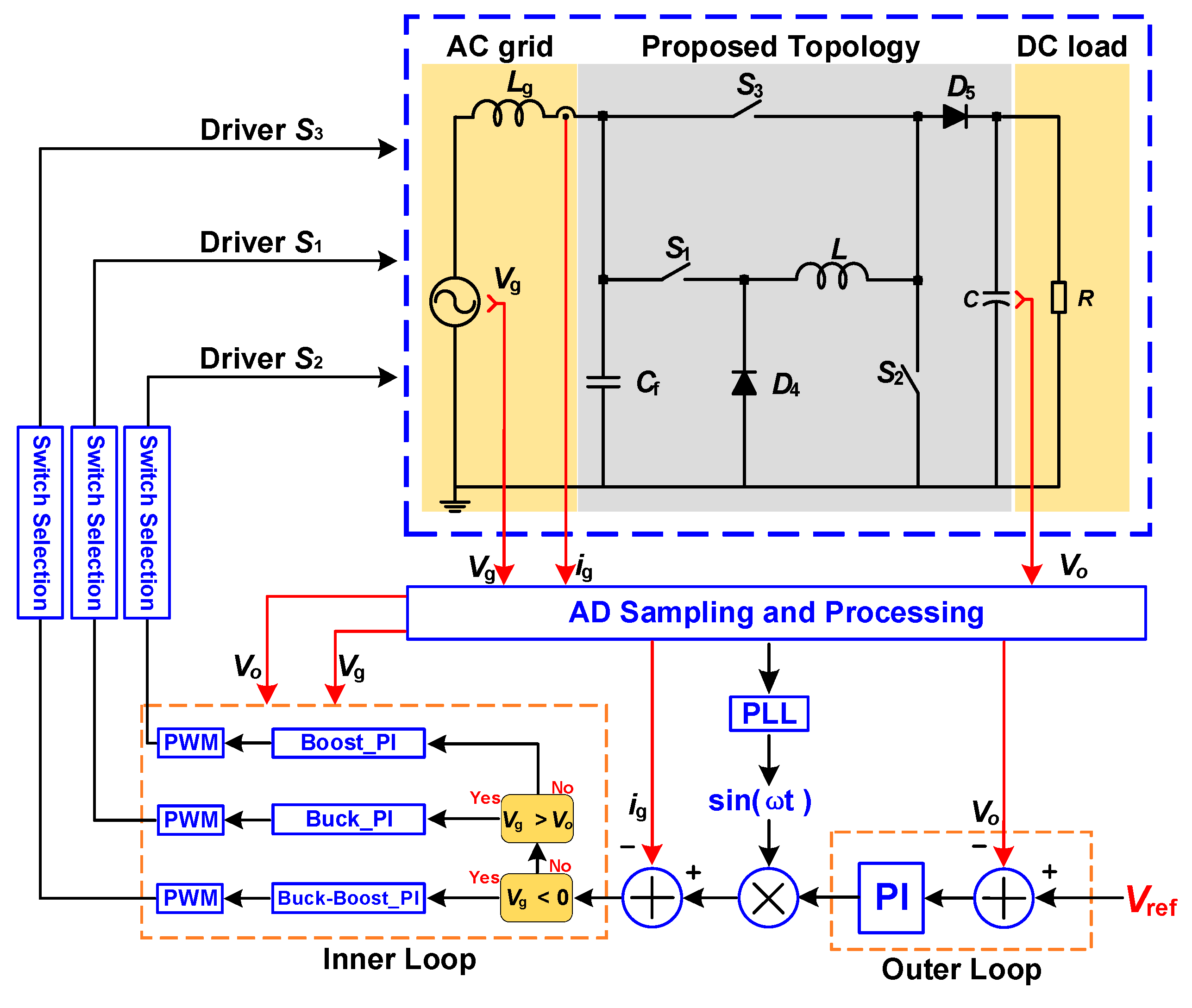
2.1. Proposed Topology
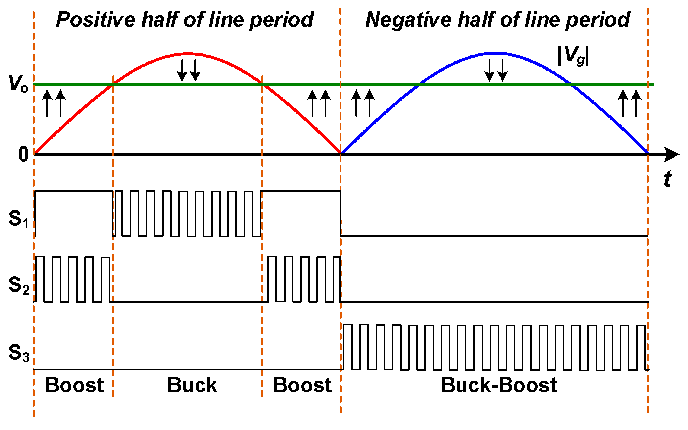
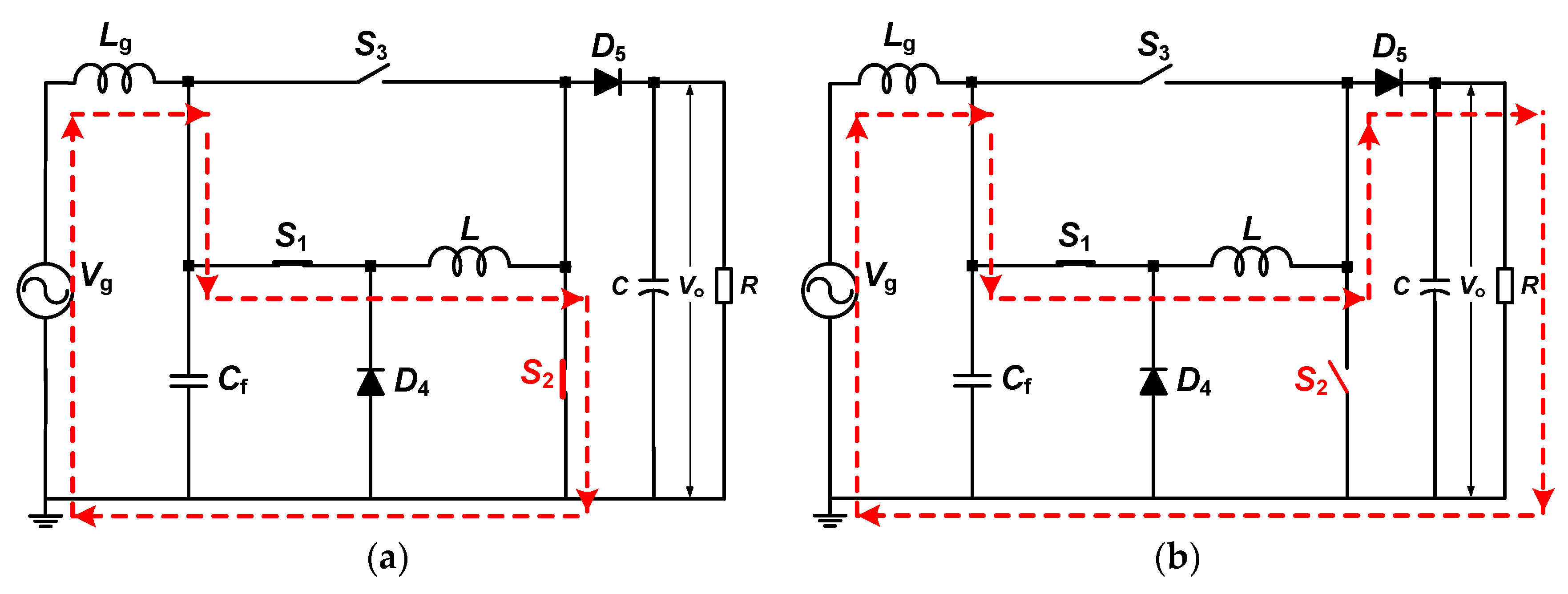
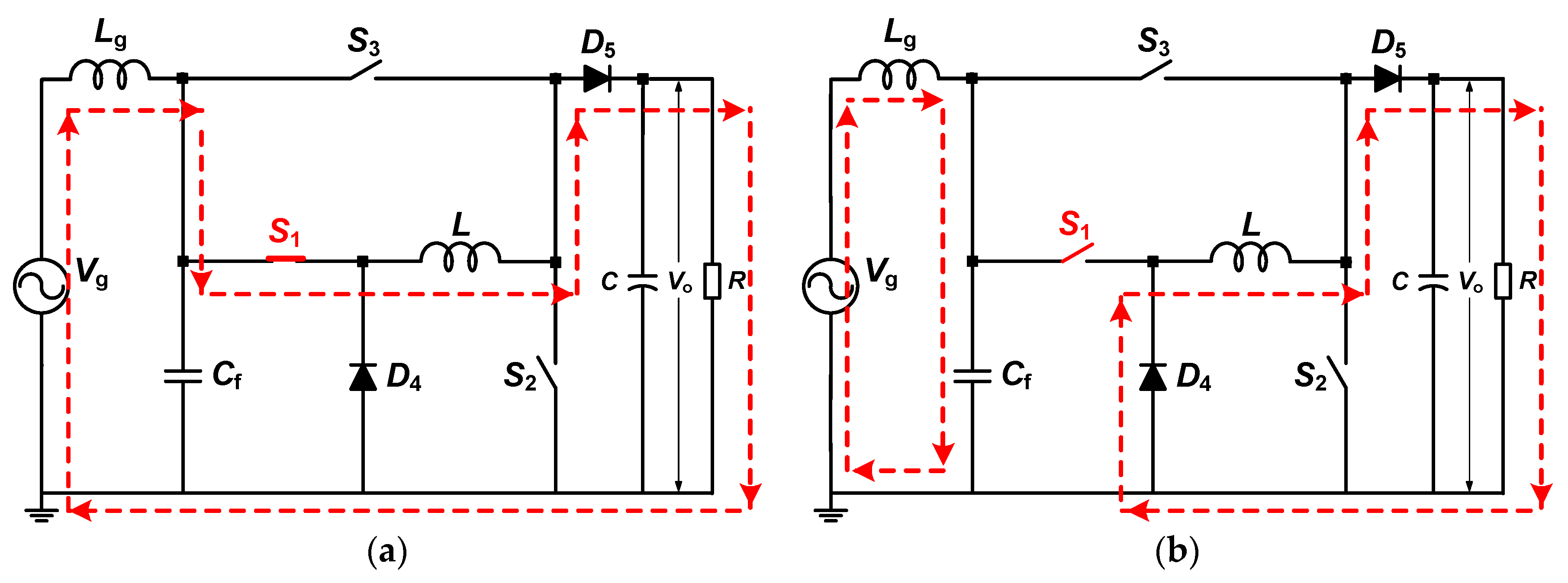
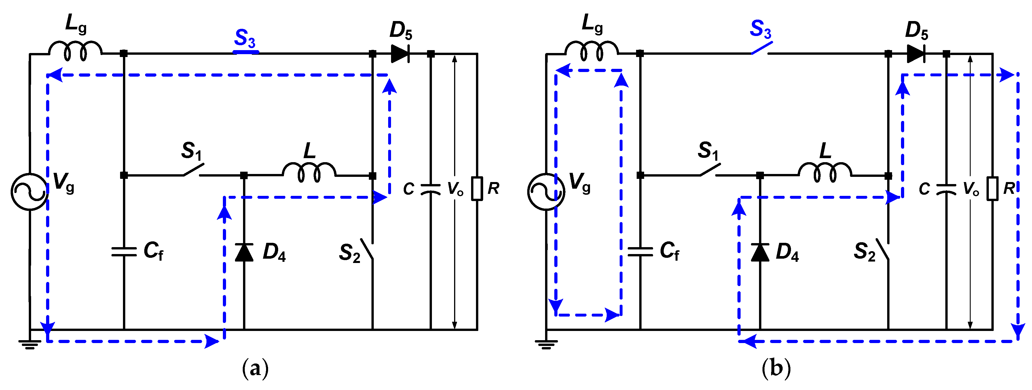
2.2. Operating Principle Description
3. Steady-State Characteristics
3.1. Grid Current
3.2. Low Frequency Voltage of the Filter Capacitor
3.3. Duty Ratio
3.4. Low Frequency Current of the DC Inductor
3.5. High Frequency Current Ripple of the DC Inductor
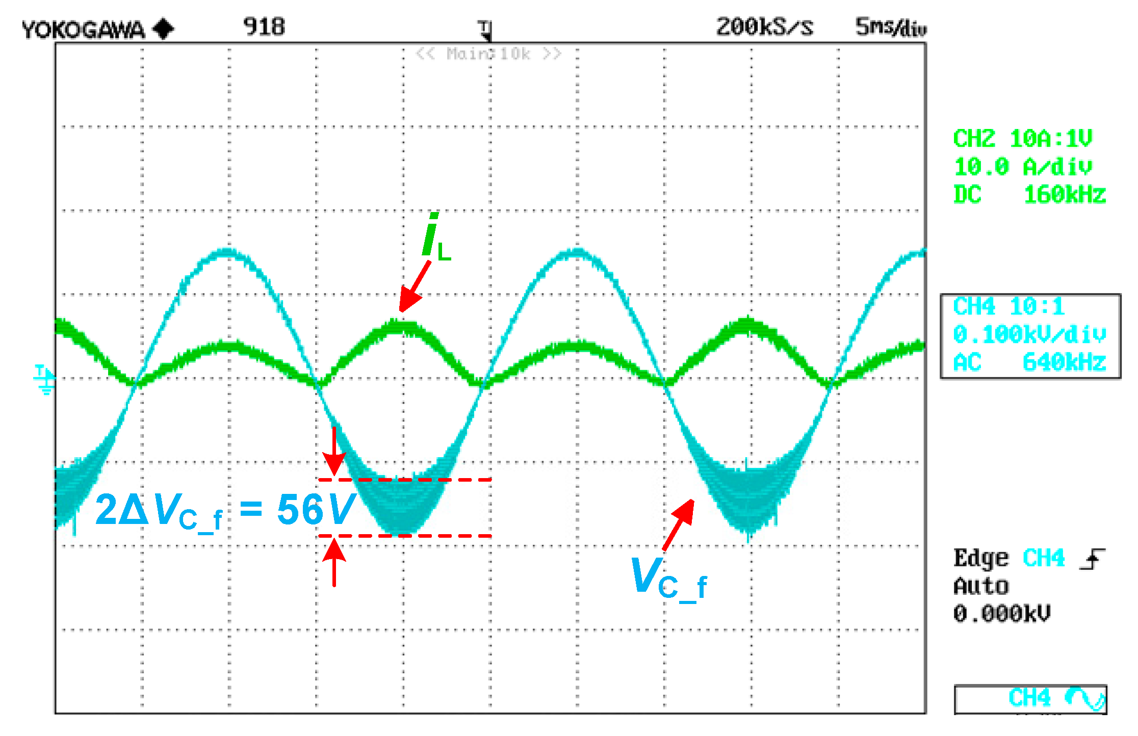
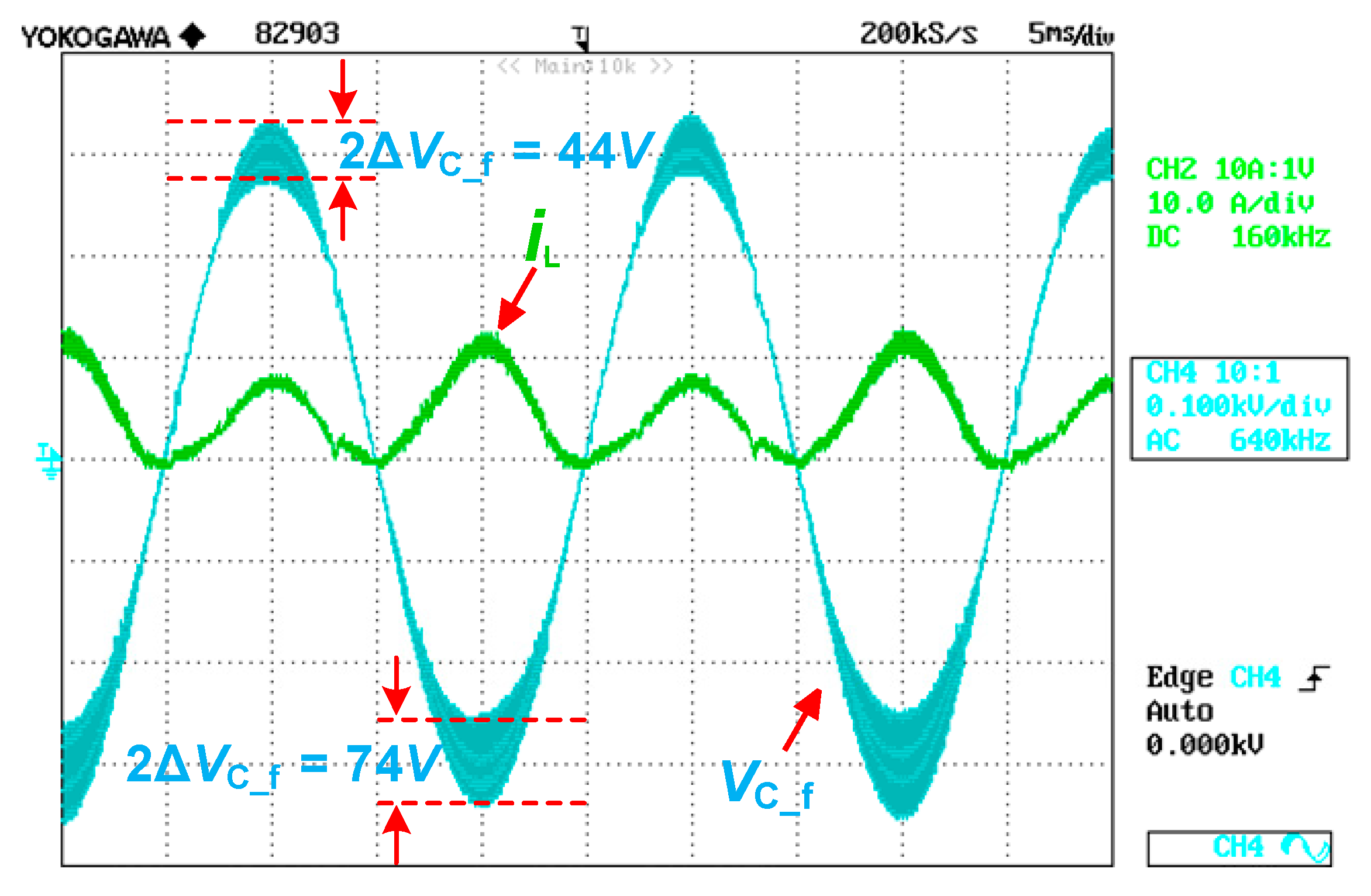
3.6. High Frequency Voltage Ripple of the Filter Capacitor
4. Small Signal Modelling and Controller Design
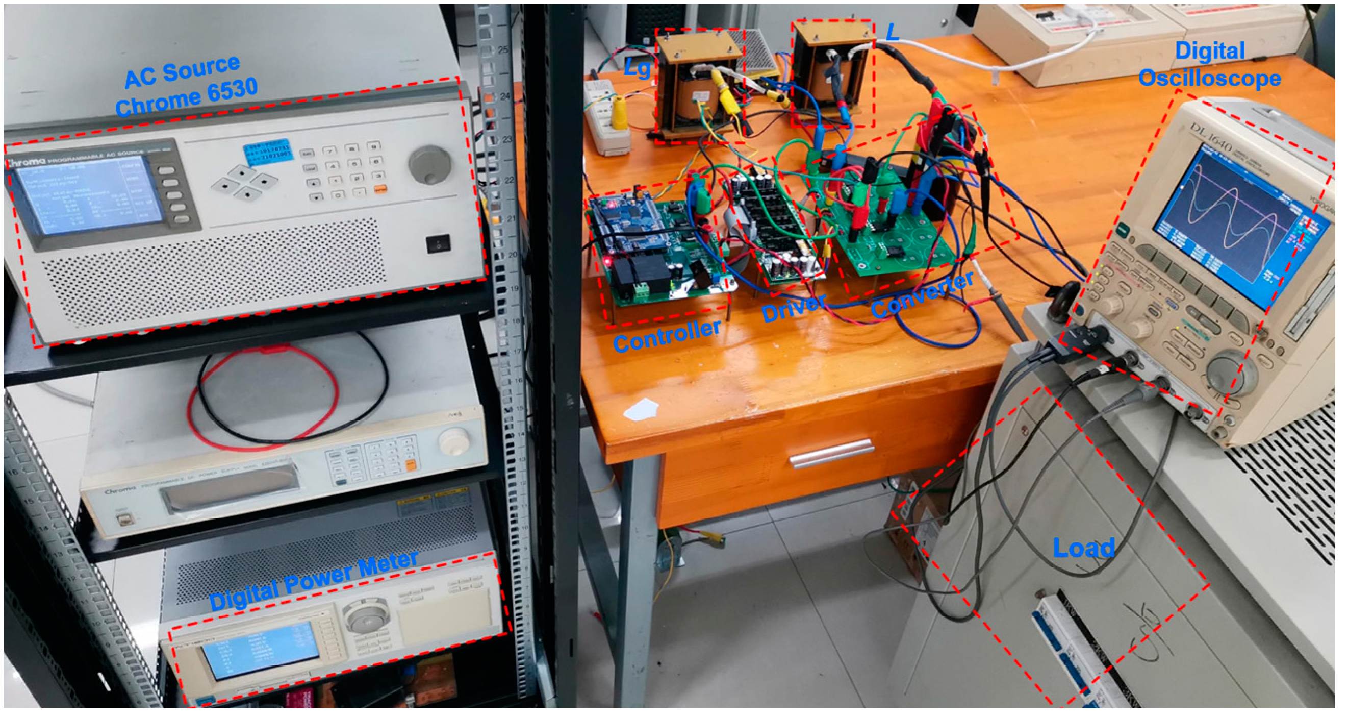
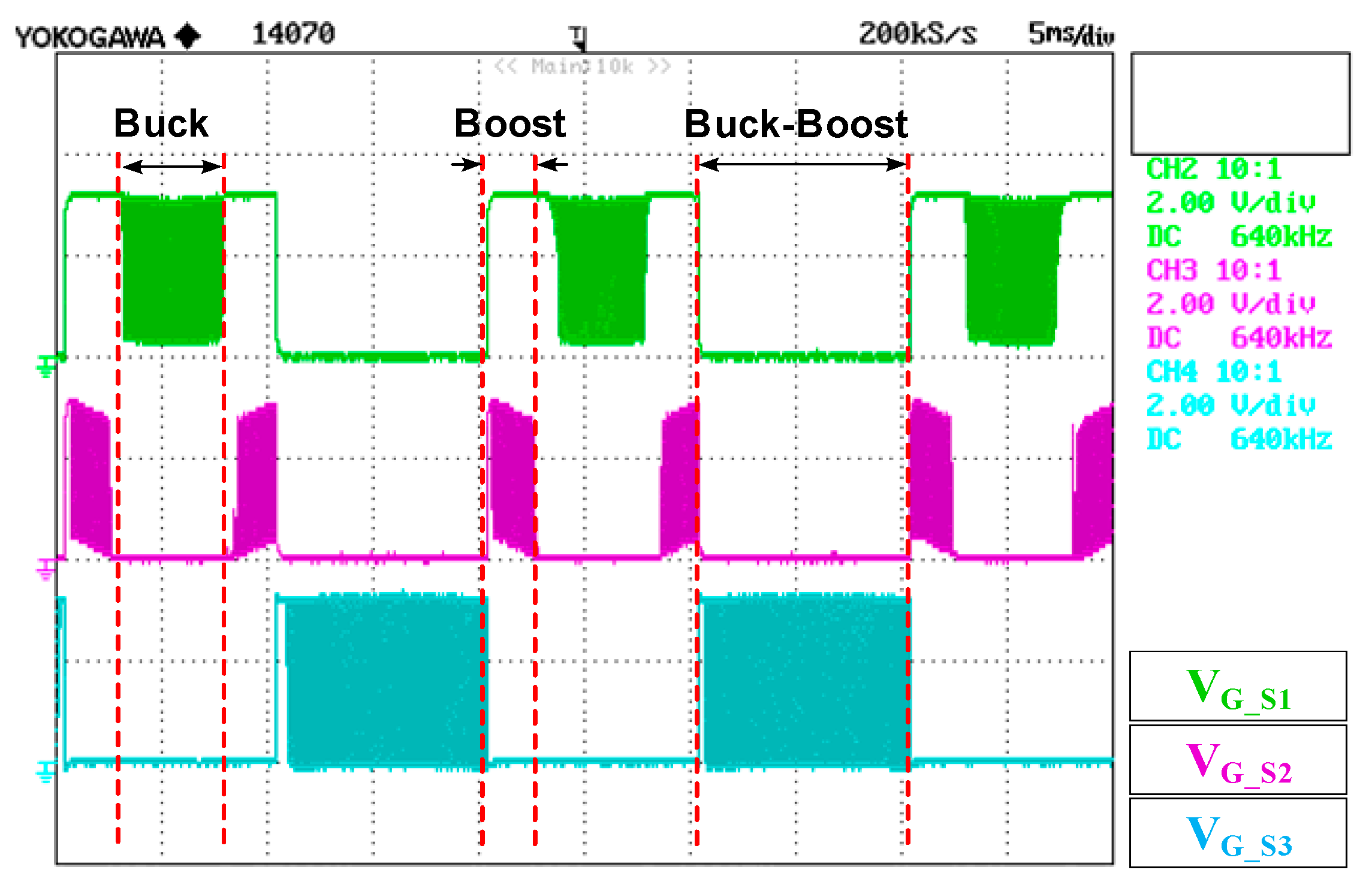
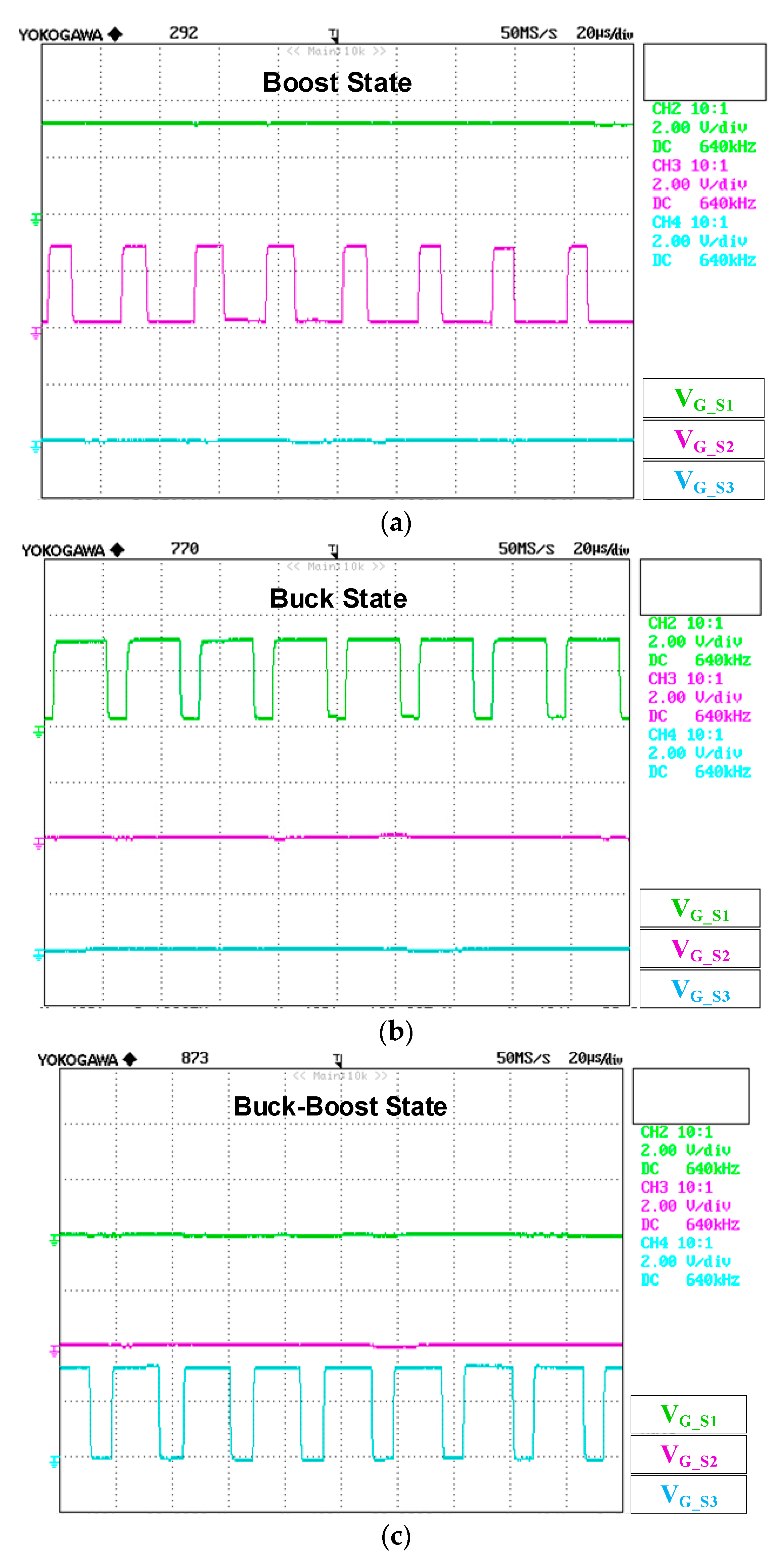
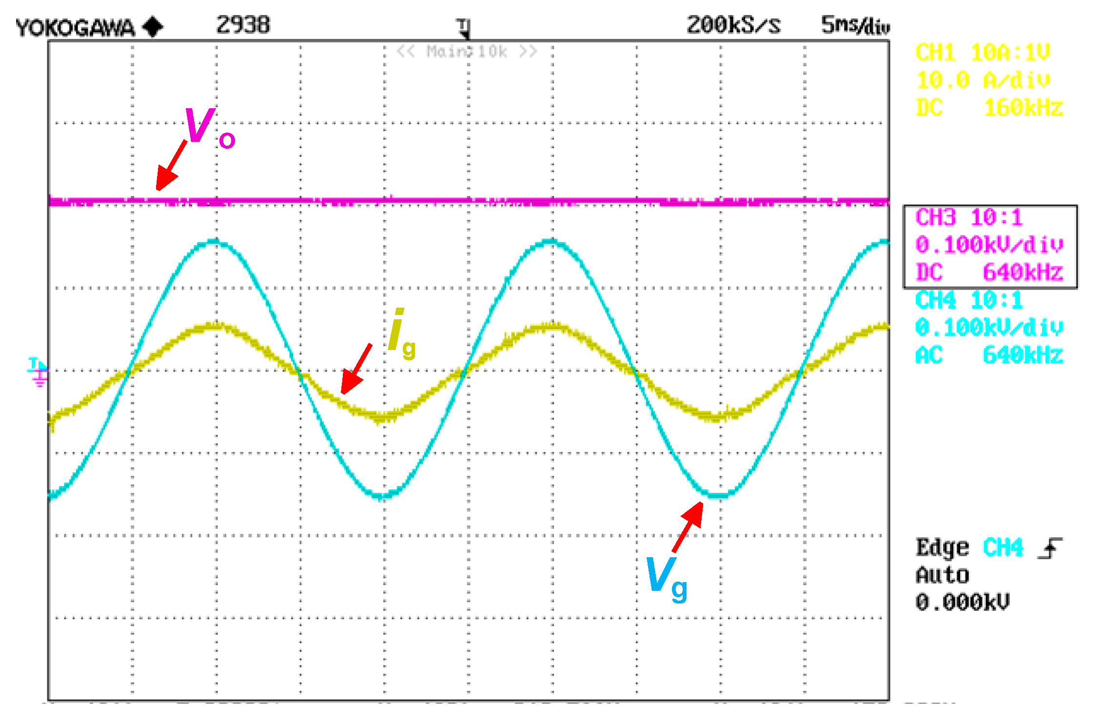
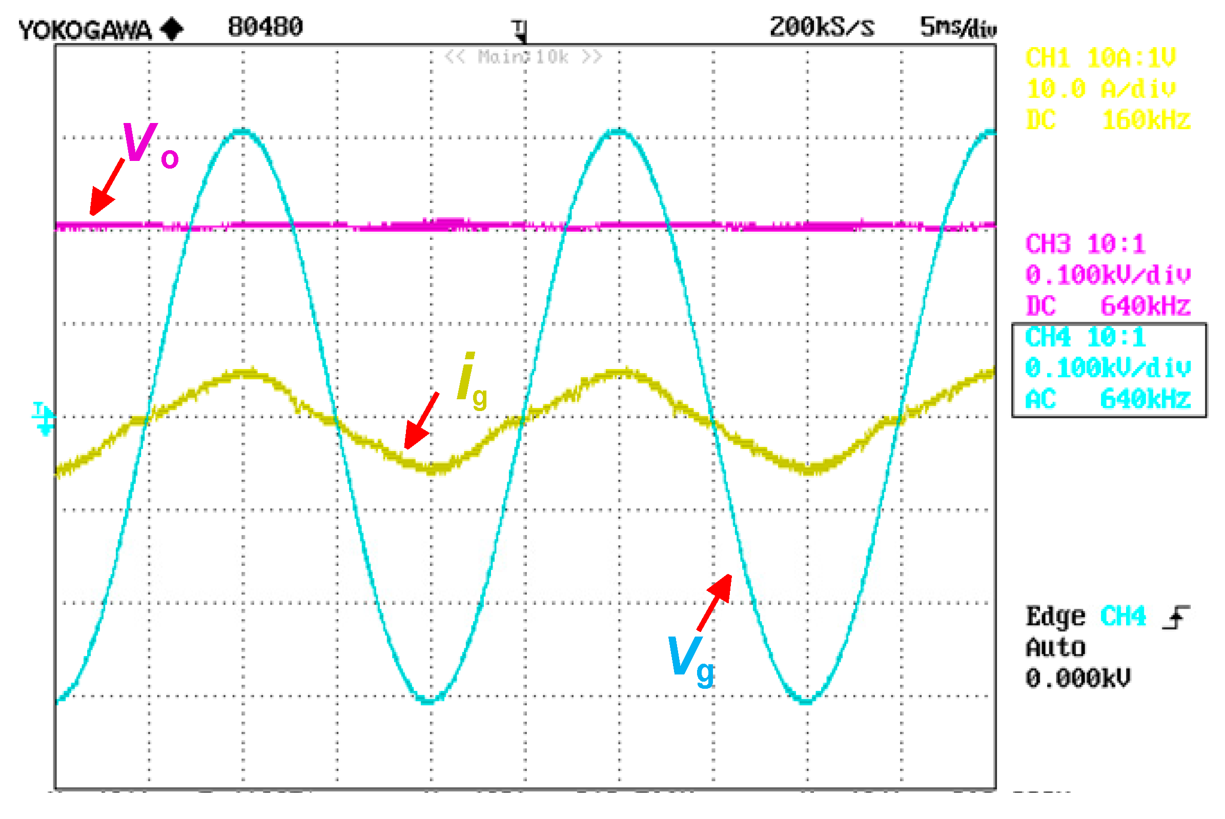
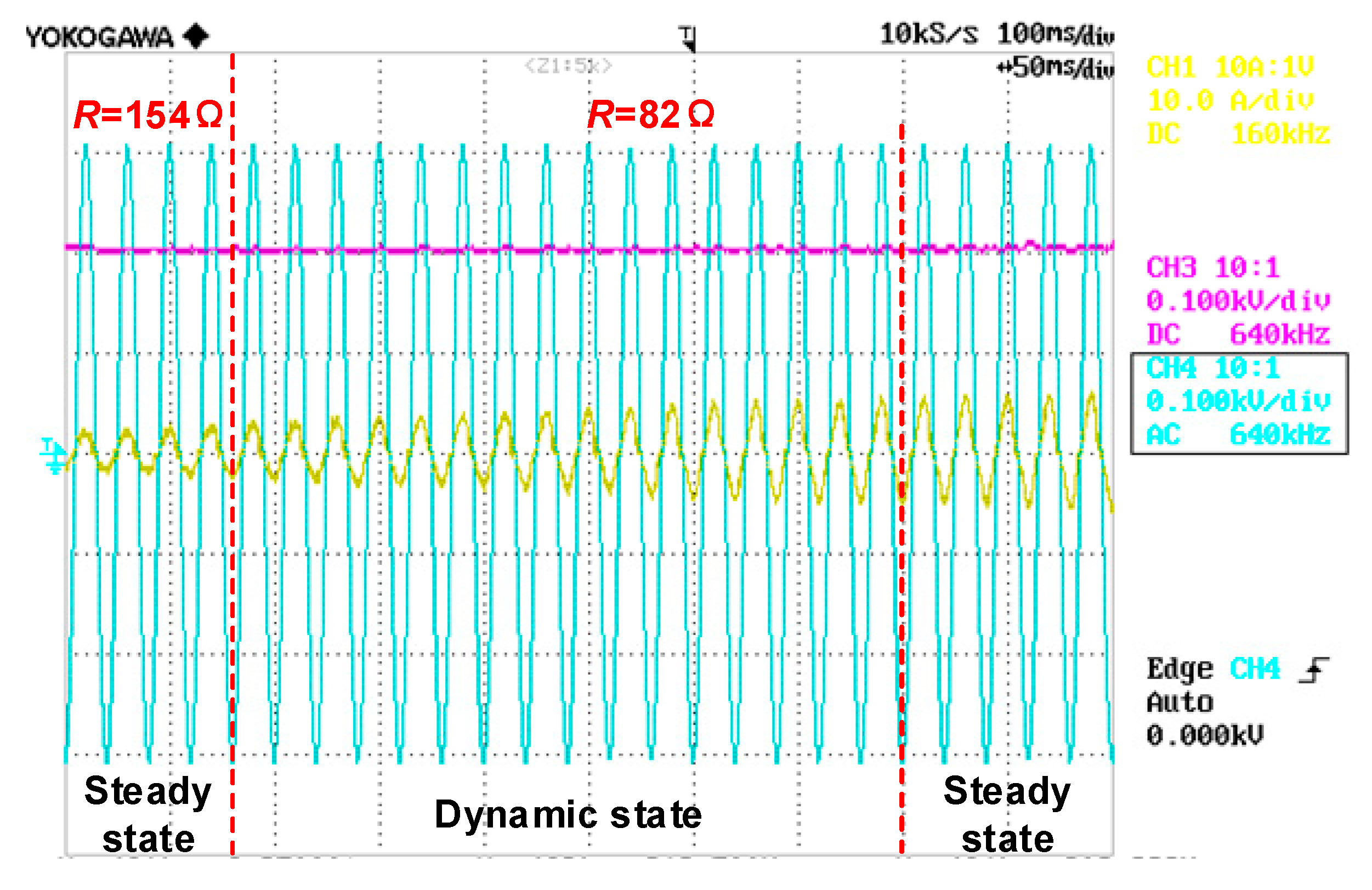
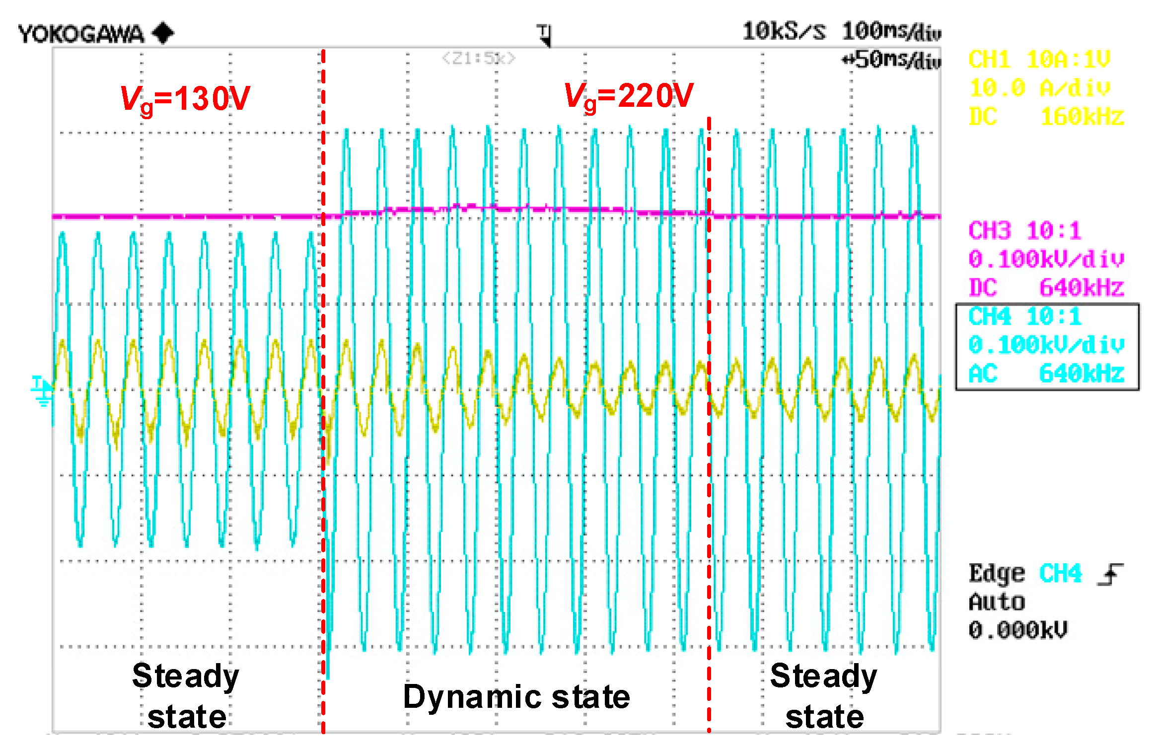
5. Experimental Results
6. Discussion
7. Conclusions
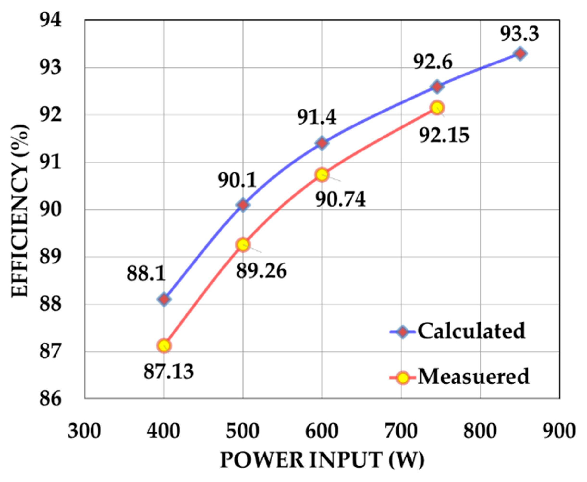
- Different from the Buck-Boost AC to DC converter presented in [10,12,13], only a single DC inductor and fewer switching devices are adopted, which can reduce the costs and volume of the system. The utilization factor of DC inductor is 100%, but it should be noted that the efficiency of the new AC to DC converter has been affected, since the new converter operates in Buck-Boost state during the negative AC grid voltage.
Author Contributions
Funding
Conflicts of Interest
Nomenclature
| Grid current | |
| Peak amplitude of grid current | |
| Grid voltage | |
| Peak amplitude of grid voltage | |
| Angular frequency of grid | |
| Voltage across the filter capacitor | |
| DC output voltage | |
| Duty ratio in “Boost” state | |
| Duty ratio in “Buck” state | |
| Duty ratio in “Buck-Boost” state | |
| Low frequency DC inductor current | |
| Voltage across the DC inductor | |
| Value of DC inductor | |
| Current ripple of the DC inductor | |
| Turn-on time in a switching period | |
| Turn-off time in a switching period | |
| Switching frequency | |
| DC inductor current ripple in “Buck” state | |
| DC inductor current ripple in “Boost” state | |
| DC inductor current ripple in “Buck-Boost” state | |
| Current of filter capacitor | |
| Value of filter capacitor | |
| Voltage ripple peak to peak value of the filter capacitor | |
| Voltage ripple peak to peak value of the filter capacitor in “Buck” state | |
| Voltage ripple peak to peak value of the filter capacitor in “Buck-Boost” state | |
| DS1 | Duty cycle of the switch S1 |
| DS3 | Duty cycle of the switch S3 |
References
- Sannino, A.; Postiglione, G.; Bollen, M.H.J. Feasibility of a DC network for commercial facilities. IEEE Trans. Ind. Appl. 2003, 39, 1499–1507. [Google Scholar] [CrossRef]
- Salomonsson, D.; Sannino, A. Low-voltage DC distribution system for commercial power systems with sensitive electronic loads. IEEE Trans. Power Deliv. 2007, 22, 1620–1627. [Google Scholar] [CrossRef]
- Sathyan, S.; Suryawanshi, H.M.; Shitole, A.B.; Ballal, M.S.; Borghate, V.B. Soft Switched Interleaved DC/DC Converter as front-end of Multi Inverter Structure for Micro Grid Applications. IEEE Trans. Power Electron. 2018, 33, 7645–7655. [Google Scholar] [CrossRef]
- Kinhekar, N.; Padhy, N.P.; Li, F.; Gupta, H.O. Utility Oriented Demand Side Management Using Smart AC and Micro DC Grid Cooperative. IEEE Trans. Power Syst. 2016, 31, 1151–1160. [Google Scholar] [CrossRef]
- Prabhakaran, P.; Goyal, Y.; Agarwal, V. Novel Nonlinear Droop Control Techniques to Overcome the Load Sharing and Voltage Regulation Issues in DC Microgrid. IEEE Trans. Power Electron. 2018, 33, 4477–4487. [Google Scholar] [CrossRef]
- Xu, Q.; Hu, X.; Wang, P.; Xiao, J.; Tu, P.; Wen, C.; Lee, M. A Decentralized Dynamic Power Sharing Strategy for Hybrid Energy Storage System in Autonomous DC Microgrid. IEEE Trans. Ind. Electron. 2017, 64, 5930–5941. [Google Scholar] [CrossRef]
- Yue, X.; Boroyevich, D.; Lee, F.C.; Chen, F.; Burgos, R.; Zhuo, F. Beat Frequency Oscillation Analysis for Power Electronic Converters in DC Nanogrid Based on Crossed Frequency Output Impedance Matrix Model. IEEE Trans. Power Electron. 2018, 33, 3052–3064. [Google Scholar] [CrossRef]
- Yang, Q.; Jiang, L.; Zhao, H.; Zeng, H. Autonomous Voltage Regulation and Current Sharing in Islanded Multi-inverter DC Microgrid. IEEE Trans. Smart Grid 2018, 9, 6429–6437. [Google Scholar] [CrossRef]
- Cai, W.; Jiang, L.; Liu, B.; Duan, S.; Zou, C. A Power Decoupled Method Based on Four-Switch Three-Port DC/DC/AC Converter in DC Microgrid. IEEE Trans. Ind. Appl. 2015, 51, 336–343. [Google Scholar] [CrossRef]
- Wu, W.; Wang, H.; Liu, Y.; Huang, M.; Blaabjerg, F. A Dual-Buck–Boost AC/DC Converter for DC Nanogrid with Three-Terminal Outputs. IEEE Trans. Ind. Electron. 2017, 64, 295–299. [Google Scholar] [CrossRef]
- Rivera, S.; Wu, B.; Kouro, S.; Yaramasu, V.; Wang, J. Electric Vehicle Charging Station Using a Neutral Point Clamped Converter With Bipolar DC Bus. IEEE Trans. Ind. Electron. 2015, 62, 1999–2009. [Google Scholar] [CrossRef]
- Wang, H.; Wu, W.; Li, Y.W.; Blaabjerg, F. A Coupled-Inductor-Based Buck-Boost AC/DC Converter with Balanced DC Output Voltages. IEEE Trans. Power Electron. 2019, 34, 151–159. [Google Scholar] [CrossRef]
- Wang, H.; Wu, W.; Gao, N.; He, Y.; Chung, H.S.; Blaabjerg, F. Modified dual buck–boost AC/DC converter with self-balanced DC output voltages. IET Power Electron. 2019, 12, 1170–1178. [Google Scholar] [CrossRef]
- Park, J.D.; Candelaria, J. Fault Detection and Isolation in Low-Voltage DC-Bus Microgrid System. IEEE Trans. Power Deliv. 2013, 28, 779–787. [Google Scholar] [CrossRef]
- Salomonsson, D.; Soder, L.; Sannino, A. Protection of Low-Voltage DC Microgrids. IEEE Trans. Power Deliv. 2009, 24, 1045–1053. [Google Scholar] [CrossRef]
- Singh, B.; Singh, B.N.; Chandra, A.; Al-Haddad, K.; Pandey, A.; Kothari, D.P. A review of single-phase improved power quality AC-DC converters. IEEE Trans. Ind. Electron. 2003, 50, 962–981. [Google Scholar] [CrossRef]
- Singh, B.; Singh, B.N.; Chandra, A.; Al-Haddad, K.; Pandey, A.; Kothari, D.P. A review of three-phase improved power quality AC-DC converters. IEEE Trans. Ind. Electron. 2004, 51, 641–660. [Google Scholar] [CrossRef]
- Jovanovic, M.M.; Jang, Y. State-of-the-art, single-phase, active power-factor-correction techniques for high-power applications—An overview. IEEE Trans. Ind. Electron. 2005, 52, 701–708. [Google Scholar] [CrossRef]
- Kolar, J.W.; Friedli, T. The Essence of Three-Phase PFC Rectifier Systems—Part I. IEEE Trans. Power Electron. 2013, 28, 176–198. [Google Scholar] [CrossRef]
- Friedli, T.; Hartmann, M.; Kolar, J.W. The Essence of Three-Phase PFC Rectifier Systems—Part II. IEEE Trans. Power Electron. 2014, 29, 543–560. [Google Scholar] [CrossRef]
- Wu, W.; Liu, Y.; Wang, H.; Huang, M.; Blaabjerg, F. Modelling and control design of a dual Buck-Boost AC/DC converter used in the DC Nano-grid. In Proceedings of the IEEE 8th International Power Electronics and Motion Control Conference (IPEMC-ECCE Asia), Hefei, China, 22–26 May 2016; pp. 2187–2192. [Google Scholar]
- Liu, Y.; Wu, W.; He, Y.; Lin, Z.; Blaabjerg, F.; Chung, H.S. An Efficient and Robust Hybrid Damper for LCL- or LLCL-based Grid-Tied Inverter with Strong Grid-side Harmonic Voltage Effect Rejection. IEEE Trans. Ind. Electron. 2016, 63, 926–936. [Google Scholar] [CrossRef]
- Wang, J.; Yan, J.D.; Jiang, L.; Zou, J. Delay-Dependent Stability of Single-Loop Controlled Grid-Connected Inverters with LCL Filters. IEEE Trans. Power Electron. 2016, 31, 743–757. [Google Scholar] [CrossRef]
- Wang, H.; Wu, W.; Zhang, S.; He, Y.; Chung, H.S.; Blaabjerg, F. A modified Aalborg inverter extracting maximum power from one PV array source. CPSS Trans. Power Electron. Appl. 2019, 4, 109–118. [Google Scholar] [CrossRef]
- Fang, J.; Li, X.; Yang, X.; Tang, Y. An Integrated Trap-LCL Filter with Reduced Current Harmonics for Grid-Connected Converters Under Weak Grid Conditions. IEEE Trans. Power Electron. 2017, 32, 8446–8457. [Google Scholar] [CrossRef]
- Wu, W.; Liu, Y.; He, Y.; Chung, H.S.; Liserre, M.; Blaabjerg, F. Damping Methods of Resonances Caused by LCL-Filter-Based Current-Controlled Grid-tied Power Inverters: An Overview. IEEE Trans. Ind. Electron. 2017, 64, 7402–7413. [Google Scholar] [CrossRef]

| Parameters | Value |
|---|---|
| Grid inductance Lg | 0.6 mH |
| Filter capacitance Cf | 2 μF |
| DC inductance L | 1.2 mH |
| DC output capacitor C | 5600 μF |
| Grid voltage Vg | 220 V |
| Grid frequency f0 | 50 Hz |
| DC output voltage Vo | 200 V |
| Input power Pin | 750 W |
| Switching frequency fsw | 40 kHz |
| Devices | Type |
|---|---|
| Switches S1–S3 | IPW65R041CFD |
| Diodes D1–D5 | IDW30G65C5 |
| Capacitor Cf | IKC CBB22 |
| Core of the inductors | EE110 |
| Topology | Converter in [10] | Converter in [12] | Converter in [13] | Proposed Converter | |
|---|---|---|---|---|---|
| Switches | 4 | 6 | 4 | 3 | |
| Diodes | 6 | 6 | 6 | 5 | |
| Capacitor | 3 | 3 | 3 | 2 | |
| DC inductors | 2 | 2 | 2 | 1 | |
| Operating states | Buck, Boost | Buck, Boost, Flybuck, Flyback | Buck, Boost, Flybuck, Flyback | Buck, Boost, Buck-Boost | |
| Utilization factor of DC inductor | 50% | 50–100% | 50–100% | 100% | |
| Complexity of small-signal models | Three-order | ||||
| Reference DC output voltage | Vo_ref = 400 V | Vo_ref = 200 V | |||
| Vg = 110V. | Loads | RL1 = 144 Ω, RL2 = 94 Ω | R = 110 Ω | ||
| Vo1 | 223.67 V | 200.86 V | 200.90 V | Vo = 200 V | |
| Vo2 | −176.43 V | −198.69 V | −198.61 V | ||
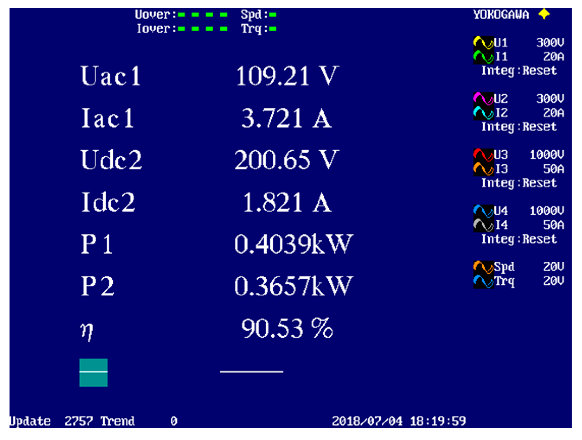
| Efficiency | 95.45% | 92.96% | 93.37% | 90.53% | |
| Vg = 220V. | Loads | RL1 = 72 Ω, RL2 = 52 Ω. | R = 60 Ω | ||
| Vo1 | 221.08 V | 203.33 V | 202.94 V | Vo = 200 V | |
| Vo2 | −179.37 V | −196.14 V | −197.35 V | ||
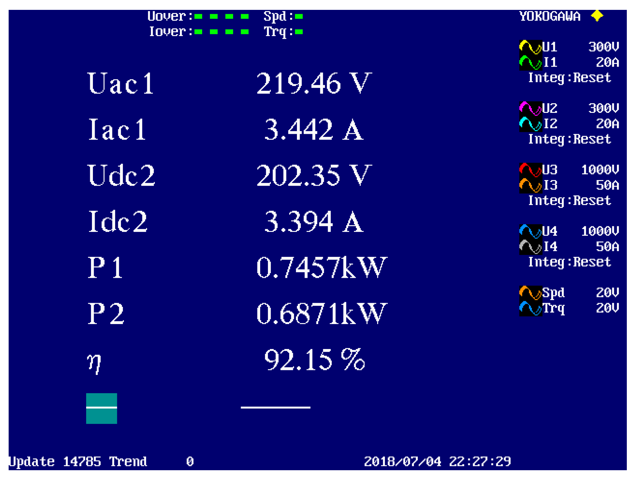
| Efficiency | 96.24% | 96.22% | 96.33% | 92.15% | |
© 2019 by the authors. Licensee MDPI, Basel, Switzerland. This article is an open access article distributed under the terms and conditions of the Creative Commons Attribution (CC BY) license (http://creativecommons.org/licenses/by/4.0/).
Share and Cite
Li, X.; Wu, W.; Wang, H.; Gao, N.; Chung, H.S.-h.; Blaabjerg, F. A New Buck-Boost AC/DC Converter with Two-Terminal Output Voltage for DC Nano-Grid. Energies 2019, 12, 3808. https://doi.org/10.3390/en12203808
Li X, Wu W, Wang H, Gao N, Chung HS-h, Blaabjerg F. A New Buck-Boost AC/DC Converter with Two-Terminal Output Voltage for DC Nano-Grid. Energies. 2019; 12(20):3808. https://doi.org/10.3390/en12203808
Chicago/Turabian StyleLi, Xiangkun, Weimin Wu, Houqing Wang, Ning Gao, Henry Shu-hung Chung, and Frede Blaabjerg. 2019. "A New Buck-Boost AC/DC Converter with Two-Terminal Output Voltage for DC Nano-Grid" Energies 12, no. 20: 3808. https://doi.org/10.3390/en12203808
APA StyleLi, X., Wu, W., Wang, H., Gao, N., Chung, H. S.-h., & Blaabjerg, F. (2019). A New Buck-Boost AC/DC Converter with Two-Terminal Output Voltage for DC Nano-Grid. Energies, 12(20), 3808. https://doi.org/10.3390/en12203808