Abstract
An efficient way of synthesizing a three port non-isolated converter from a single-ended primary inductor converter (SEPIC) is proposed in this paper. The primary SEPIC converter is split into a source cell and a load cell. Two such source cells are integrated through direct current (DC) link capacitors with a common load cell to generate a three-port SEPIC converter. The derived converter features single-stage power conversion with reduced structural complexity and bidirectional power flow capability. For bidirectional power flow, it incorporates a battery along with an auxiliary photovoltaic source. Mathematical analyses were carried out to describe the operating principles and design considerations. Experiments were performed on an in-house-built prototype three-port unidirectional converter, and the results are presented to validate the feasibility of the designed converter.
1. Introduction
Renewable energy resources are of potential interest nowadays due to environmental problems, high oil prices, global warming, and the depletion of fossil fuels. Though these renewable energy resources are abundant and cause zero emissions, they are intermittent in nature. When integrating, these power generators provide low voltage and require high-gain converters to meet the load demand. Thus, power electronic technology plays a significant role in interfacing hybrid renewable power systems, electric traction, and uninterrupted power supplies [1,2]. To overcome the intermittent nature of energy resources, future power systems will also require the interfacing of various energy sources using multisource technology. To enable multi-source technology, a multi-input power converter (MIPC) that can accommodate a variety of sources, as shown in Figure 1, seems to be essential. A few limitations in this structure are as follows:
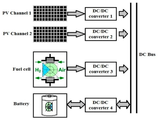
Figure 1.
Conventional multi-input converter.
- MIPCs utilize separate direct current (DC)–DC power converters to integrate diversified energy sources to a common DC bus, which results in a higher implementation cost.
- In the case of alternating current (AC) loads, the system needs an extra inverter, and as a result the efficiency is reduced.
Due to the above disadvantages, the implementation of a MIPC is complicated.
To overcome the drawbacks of MIPCs, such as structure complications, multi-port converters (MPC) have been proposed. In MPCs, various sources are fed to the load through a single power electronic converter, as shown in Figure 2. MPCs reduce the structural complexity and the control technique.
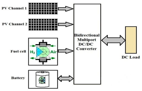
Figure 2.
The multiport structure.
These power electronic converters can be classified based on:
- Topology (in series and parallel)
- Coupling (isolated and non-isolated)
- Port placement (single input–single output, multi-input–single output, multi-input–multi-output, and single input–multi-output)
- Conversion process (unidirectional and bidirectional)
Two input circuits with a current source connected in series to realize a high-efficiency, zero voltage switching dual-input converter are investigated in Reference [3]. In such series circuits, the weakest current source connected in series limits the current of the entire string. Thus, parallel-connected topologies are traditionally popular. Isolated converters use a transformer to achieve a high voltage gain, which increases the bulkiness of the system and leads to core-saturation problems. To achieve a wide output voltage, an interleaved LLC converter with voltage doublers is proposed in Reference [4]. A coupled-inductor-based bidirectional converter, as investigated in Reference [5], provides a high voltage gain and efficiency by employing soft switching and voltage clamping techniques to reduce the switching loss and achieve a high voltage gain. However, the shortcoming of this converter is that current ripples are introduced, due to an increase in the ratio of the coupled inductor. It therefore requires a filter arrangement, which in turn increases the structural complexity and the cost. To overcome the need for a filter requirement, a (non-isolated) converter without galvanic isolation is a good candidate to provide a large voltage gain with reduced size and cost. Such a single-stage Zeta single-ended primary inductor converter (SEPIC) converter is presented in Reference [6]. A high-gain, non-isolated DC–DC converter is analyzed in Reference [7]. A step-up converter combining the features of a KY converter and a buck–boost converter with a high voltage conversion ratio is presented in Reference [8]. A non-isolated, bidirectional DC–DC converter that uses four active switches is addressed in Reference [9]. A SEPIC-integrated boost converter with isolation, proposed in Reference [10], has one active switch, two inductors, and three capacitors. The above-mentioned converters are unidirectional, with a single input–single output (SISO) configuration. A systematic way of deriving MPCs using full bridge (FB) and bidirectional DC–DC converters (BDCs) is explained in Reference [11]. Various configurations of multiport converters using a DC link inductor are well-described in Reference [12]. A new multi-input DC–DC converter topology that is capable of integrating diversified energy resources of different voltage–current characteristics is proposed in Reference [13]. The setback for this converter is that only one input is allowed to transfer energy into the load at a time in boost mode. The concept of extracting pulsating source cells from basic converters like buck, boost, buck–boost, Zeta, Cuk, and SEPIC is reported in Reference [14].
A dual-input boost–buck converter with a coupled inductor is analyzed in Reference [15]. Though the presence of the coupled inductor causes current ripples, the interleaving mode operation of the converter reduces the ripples and makes the converter suitable for thermoelectric generator application. Integrated two input converters using buck and SEPIC topology are addressed in Reference [16]. A generic structure of a single-ended primary-inductor converter (SEPIC)-based multi (m)-input DC–DC converter is investigated in Reference [17]. This converter utilizes (m-2) +3 switches to interface ‘m’ input resources. For example, four active switches are required for realization of a three input structure of this converter. A single input–multi-output structure converter with the ability of generating buck, boost, and inverted output simultaneously is presented in Reference [18]. The drawback of this converter is that it is a single input–multi-output (SIMO) model, capable of interfacing only one input. The unified energy management scheme dealt with in Reference [19] employs different current control structures for various components of micro-grids, such as super capacitors, battery, renewable energy resources (RES), and voltage source converters (VSC). A power flow management control strategy based on sensing the battery voltage to select the operating modes of a bidirectional converter is presented in Reference [20]. A multiport power electronic interface as energy router with inductively coupled power transfer, ultra-capacitor and battery to solve the pulse charging is investigated in Reference [21]. Power budgeting using DC link voltage and current control methods have been analyzed in Reference [22].
To overcome drawbacks such as the size and control complexity due to the isolated transformer and a greater number of components, and to have a flexible integration of the diversified energy resources of different characteristics, a compact, high-profile power electronic interface is required. Most of the multi-input converter (MIC) topologies in the literature are derived from basic buck–boost topologies, and they leave scope for the further development of topological structures by using special converters. Therefore, this paper proposes a modular, non-isolated converter that is derived from basic SEPIC topology for accommodating arbitrary input sources and output loads. Due to special features, such as a better power factor from a continuous input current, non-inverting output, gracious response, and true shut down during short circuits, this SEPIC converter has wide applications in connecting flexible input voltages with stable outputs, battery-operated equipment, and lighting applications.
2. Three-Port SEPIC Converter
2.1. Synthesis of the Three-Port SEPIC Converter
A generalized structure of the proposed circuit is shown in Figure 3. It indicates that the number of ports can be further increased/decreased by connecting/disconnecting the additional pulsating voltage cells (PVC), depending on the availability of the sources.
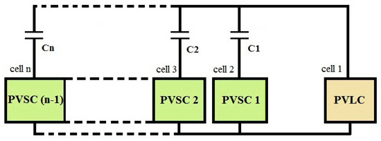
Figure 3.
Generalized diagram of an n-port SEPIC converter.
In this paper, three-port (two inputs and one output) unidirectional and bidirectional SEPIC converters are proposed, as shown in Figure 4 and Figure 9. The proposed structures are a combination of PVC. PVCs can be categorized into two types; pulsating voltage source cells (PVSC) for the input side, and pulsating voltage load cell (PVLC) for the output side. Each PVSC connects with a common PVLC (as it is a MISO structure) through a coupling capacitor, and this forms a complete SEPIC structure.
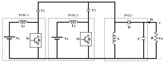
Figure 4.
A three-port unidirectional SEPIC converter (Topology-1).
2.1.1. Steady State Analysis of a Three-Port Unidirectional SEPIC Converter (Topology-1)
In topology-1, if both sources are renewable DC sources; for example, if V1 is a solar photovoltaic system and if V2 is a fuel cell, then the converter works as a unidirectional converter, as the energy flows only from the source to the load. If both sources have an equal voltage magnitude, then the switches S1 and S2 operate with the same duty cycle simultaneously. If the primary source is a solar photovoltaic system and the secondary source is an energy storage device, then it works as a partially bidirectional converter. The reason for partial bidirectional is that the battery will charge from the primary source if the battery nominal voltage is less than the primary source voltage. To charge the battery, the switch in the corresponding PVSC has to be permanently turned off, and only the switches of other PVSCs will operate. Figure 4 shows the circuit diagram of a three-port unidirectional SEPIC converter.
If two DC voltage sources with different magnitudes, V1 and V2, are considered, then in order to use the sources effectively, the two sources must operate at different duty cycles. The source with a higher magnitude operates for the lower duty cycles, and the source with the lower magnitude operates for a higher duty cycle.
Assuming that V1 > V2, then D1 < D2. D1 and D2 are the respective duty cycles for PVSC1 and PVSC2. The operation of the three-port unidirectional SEPIC converter (Topology-1) is categorized into three modes, as shown in Figure 5.
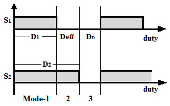
Figure 5.
Modes of operation.
Where Deff is the effective duty of PVSC2, Deff = D2 − D1, and DD is the duty for which the diode conducts; DD = 1 − D2.
- ■
- Mode-1 (S1 and S2 ON, only S1 conducts): The equivalent circuit of Mode-1 is shown in Figure 6. Switches S1 and S2 are on during this mode. In a steady-state condition, the voltages on the input capacitors C1 and C2 are the source voltages V1 and V2, respectively. Since V1 is considered to be greater than V2, S2 blocks the possibility of a reverse current through the input leg of PVSC2. This mode makes S1 conduct the current, while S2 is reverse-biased. Since D is reverse-biased, it does not conduct, and meanwhile, the load side current is maintained by the output capacitor C.
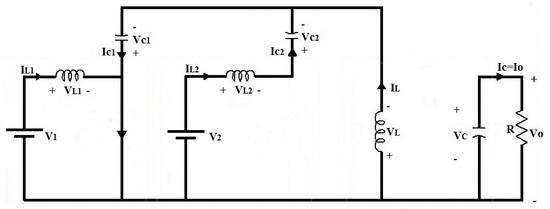 Figure 6. Mode-1 of topology-1 (S1 and S2 ON, only S1 conducts).
 - ■
- Mode-2 (S1 OFF and S2 ON): The equivalent circuit of Mode-2 is shown in Figure 7. Once the switch S1 is off, the switch S2 becomes forward-biased and starts conducting, since the duty cycle of S2 is greater than S1. Since the diode D is still in a reverse-biased condition, the load current is again maintained by the output capacitor C.
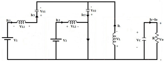 Figure 7. Mode-2 of topology-1 (S1 OFF and S2 ON).
 - ■
- Mode-3 (S1 and S2 OFF, D conducts): The equivalent circuit of Mode-3 is shown in Figure 8. Both the switches S1 and S2 are in the off-state. The inductor L1 and L2 starts discharging, and the capacitors C1 and C2 start charging from the sources V1 and V2. The diode D becomes forward-biased. The load current is now supplied by the sources V1 and V2, through L1, C1, and L2, C2, respectively.
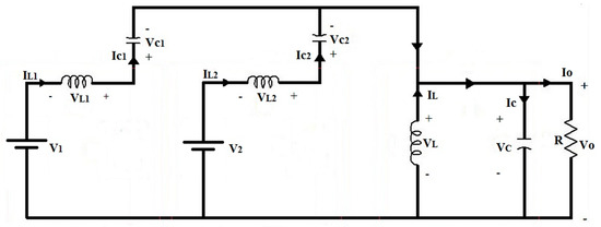 Figure 8. Mode-3 of topology-1 (S1 and S2 OFF, D conducts).
Combining the equations from (1) to (18) with their respective operating periods, the steady-state equations of the proposed unidirectional converter can be deduced as follows:
Assuming that the converter is operated in CCM, and neglecting the ripple voltage and ripple current, in a steady state average condition, VC1 = V1, VC2 = V2, and VC = VO. So, from Equation (21), we have:
The above Equation (25) represents the output voltage expression of topology-1. On solving the steady state Equations (19)–(24) by taking the left hand side as zero, the six state variables can be derived (iL1, iL2, iL, VC1, VC2, and VC):
2.1.2. Steady State Analysis of a Three-Port Bidirectional SEPIC Converter (Topology-2)
Topology-2 is designed to be a bidirectional converter with a solar photovoltaic system as a primary source, and a battery as an energy storage device. Figure 9 shows the circuit diagram of a three-port, bidirectional SEPIC converter. The converter possesses bidirectional power flow capability, as the battery can be charged both from the primary source and the regenerative energy, if it is available from the load side.
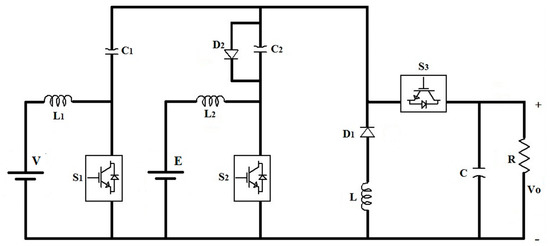
Figure 9.
Three-port bidirectional SEPIC converter (Topology-2).
For bidirectional power flow with a solar photovoltaic system (V) and a battery (E), the converter operates with two possible conditions.
Case-1 (V < E, battery discharging): Switches S1 and S2 operate with duty cycles D1 and D2 (where D1 > D2) and S3 will remain in the OFF condition. In this case, the converter operates as a unidirectional converter, i.e., in a similar fashion to that of topology-1. Figure 10 shows the modes of operation of topology-2 under this condition.
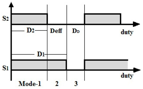
Figure 10.
Modes of operation (case 1, when V < E).
Since the converter operates in a similar fashion as that of topology-1 in this case, the output voltage expression will remain the same as topology-1:
where Deff = D1 − D2, V = primary source voltage, E = battery nominal voltage.
Case-2 (V > E, battery charging): Switch S2 will remain OFF; S1 only will operate at duty cycle D. Two modes of operation are possible in this case, as shown in Figure 11.
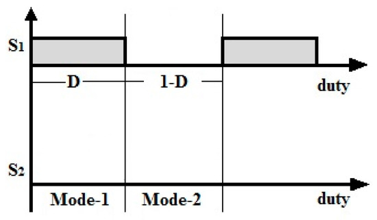
Figure 11.
Modes of operation (case 2, when V > E).
- ■
- Mode 1 (S1 ON, S2 and S3 OFF): In this mode of operation, S2 and S3 remain in an off state and S1 is on for the duty cycle D. C1 discharges energy through the short path of S1, and it flows through L and also through the anti-parallel diode of S2, and charges C2. The stored energy of L2 freewheels through the battery, and the short path makes the battery charge up. L1 charges from the source V. Meanwhile, the load is fed by the capacitor C, as the diode is reverse-biased. The equivalent circuit of this mode shown in Figure 12.
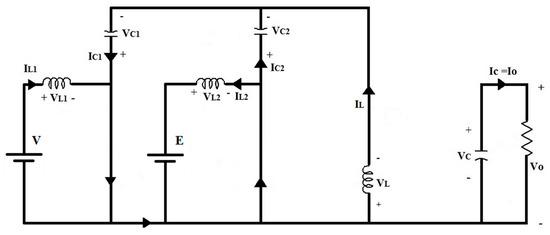 Figure 12. Mode 1 of topology-2 (case-2).
 - ■
- Mode-2 (S1 OFF, S2 OFF): In this mode of operation, S2 and S3 remain in the off state, and S1 is also in the off state for 1-D. The capacitor C1 charges from the voltage source V, and C2 discharges through the inductor L2 and the battery. This mode makes L2 store energy, and the battery charge. L1 releases stored energy through C1. The anti-parallel diode of S3 becomes forward-biased, and the load is powered up by the source and output inductor L. The equivalent circuit of this mode is shown in Figure 13.
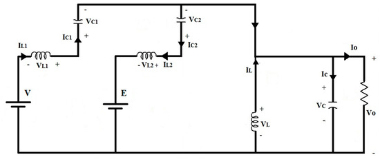 Figure 13. Mode-2 of topology-2 (case-2).
Combining the equations from (34) to (43) with their respective operating periods, the steady-state equations of the proposed bidirectional converter (case-2) can be deduced as follows:
Assuming that the converter is operated in CCM, and neglecting the ripple voltage and ripple current, in a steady-state average condition, VC1 = V, VC2 = V, and VC = VO. So, from Equation (46), we have:
The above expression (47) represents the output voltage of topology-2 while charging.
During reverse power flow, if any, the switches S1 and S2 will remain off, and only S3 will operate. If S3 is on, the current will flow from the load side to the battery (E) through D2 and L2, and the inductor L2 will store energy. If S3 is off, the inductor L2 discharges energy to the battery (E) through the anti-parallel diode of S2. This means the battery is charged from the regenerative energy, if it is available from the load side.
2.1.3. Small Ripple Approximation of a Three-Port SEPIC Converter
The methods of operation for topology-1 and topology-2 (case-1) are similar. The parameters used for topology-1 can also be used for topology-2. In this section, the expressions for all of the circuit parameters are described. Following the individual modes, the expressions for L1, L2, L, C1, C2, and C concerning the current and voltage ripples are described below.
Consider the three modes, (i.e., D1, Deff, and DD) operating for t1, t2, and t3 periods respectively.
In mode-1 and mode-2, the inductor current increases from a low level to high level, say, IL11 to IL12, and in mode-3, the current falls from IL12 to IL11. Therefore, the current ripple is considered to be ΔIL1 = IL12 – IL11. Thus:
If ‘T’ is the total period, then t1, t2, and t3 can be represented as D1T, DeffT, and DDT, respectively. Thus:
where f = 1/T, assuming that the inductor L2 charges linearly during the periods t1 and t2 from IL21 to IL22. Thus, the current ripple is ΔIL2 = IL22 − IL21.
The output side inductor L discharges from a high value to low value, say IL2 to IL1, only within period t3. Hence the ripple is ΔIL = IL2 − IL1.
Here VC = VO, so:
Similarly, the voltage ripples can be calculated from the steady-state equations. The voltage across C1 rises (assuming linearly) from a low value to a high value, say VC11 to VC12, during the time periods t2 and t3. This flow gives a voltage ripple ΔVC1 = VC12 − VC11. In this period, the capacitor is charging by the source current of V1, i.e., I1 = iL1.
The capacitor C2 is charging during period t3 and t1 from the source current V2, i.e., I2 = iL2. Therefore, a voltage ripple of ΔVC2 = VC22 − VC21 appears across capacitor C2.
The capacitor C discharges during periods t1 and t2, providing the load current. The voltage ripple is defined as ΔVC = VC2 − VC1.
Thus, the circuit parameters can be obtained from Equations (48) to (53):
3. Results Analysis
The analysis of the proposed converter is further discussed and verified in this section, through simulations for both topologies, using MATLAB/Simulink software. Table 1 indicates the parameters used in the simulation of topology-1.

Table 1.
Simulation parameters.
The permissible value of the current and voltage ripples are assumed to be ΔIL1 = ΔIL2 = ΔIL = 0.5 A, and ΔVC1= ΔVC2 = ΔVC = 0.5 V. The input voltages (V1, V2), duty cycles (D1, D2), and the corresponding values of L1, L2, L, C1, C2, and C are estimated by using Equations (54)–(59), as shown in Table 1.
Figure 14 shows the waveforms of the current and voltage through and across the inductors and capacitors, respectively. The output voltage and current of the proposed converter (topology-1) shown in Figure 15 was found to be VO = 79 V and IO = 1.3 A. The actual current and voltage ripples estimated from the simulation were approximately equal, and within the allowed value range of the ripples. The actual values of the ripples from the simulation were ΔIL1 = 0.3 A, ΔVC1 = 0.13 mV, ΔIL2 = 0.35 A, ΔVC2 = 0.4 mV, ΔIL = 0.4 A, and ΔVC = 0.4 mV.
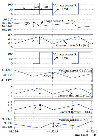
Figure 14.
Current and voltage waveforms of each component (switch, inductor, and capacitor) present in PVSC1, PVSC2, and PVLC of topology-1.
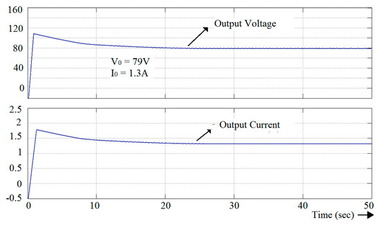
Figure 15.
Output voltage and current waveforms of topology-1.
The comparisons of the simulated output voltage (from the Simulink model) and the estimated output voltage from Equations (25) and (26) for the different sets of input voltages (V1, V2) and duty cycles (D1, D2) are shown in Table 2. The simulation and the estimated results were approximately same for each individual set of inputs.
Table 2.
Comparison of the simulated and estimated results of topology-1.
The output voltage and current waveforms of topology-2 during discharging (case-1) are shown in Figure 16. The primary source voltage was taken as V = 16 V, and the nominal battery voltage rating was E = 24 V. An initial state of charge of the battery (SOC) was considered to be 80%. The duty cycles of the primary source and the battery were assumed to be 75% and 50%, respectively. The discharging of the battery can be seen in the SOC graph, as shown in Figure 17. The SOC was decreasing in nature.
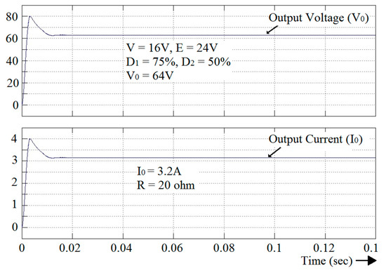
Figure 16.
Output voltage and current waveforms of topology-2 during discharging (case-1).
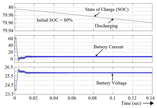
Figure 17.
State of charge, current, and voltage waveforms of battery for topology-2 during discharging (case-1).
The comparison of the simulated output voltage (from the Simulink model) and the estimated output voltage from Equation (33) for the different sets of primary inputs and battery nominal voltages (V, E) and duty cycles (D1, D2) is shown in Table 3. The simulation and estimated results were approximately the same for each individual set of inputs.
Table 3.
Comparison of the simulated and estimated results of topology-2 during discharging (case-1).
The output voltage and current waveforms of topology-2 during charging (case-2) are shown in Figure 18. The primary source voltage was taken as V = 30 V, and the nominal battery voltage rating was E = 24 V. An initial SOC was considered at 40%. The duty cycle of the primary source was assumed to be 60%, and the switch under the battery cell remained off. The charging of the battery can be seen in the SOC graph, shown in Figure 19. The SOC was increasing in nature.
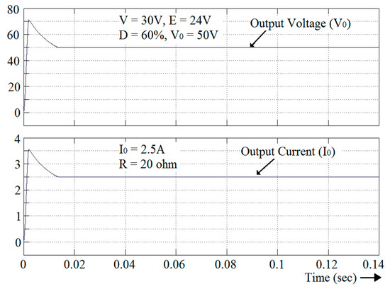
Figure 18.
Output voltage and current waveforms of topology-2 during charging (case-2).
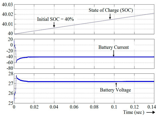
Figure 19.
State of charge (SOC), current, and voltage waveforms of the battery for topology-2 during charging (case-2).
A comparison of the simulated output voltage (from the Simulink model) and the estimated output voltage from Equation (47), for different sets of primary inputs and battery nominal voltages (V, E), and duty cycles (D1, D2) are shown in Table 4. The simulation and estimated results were approximately same for each individual set of inputs.
Table 4.
Comparison of the simulated and estimated results of topology-2 during charging (case-2).
4. Design of Controllers for the Three-Port SEPIC Converter
A controller is needed for closed loop operation of the proposed converter, in order to maintain the output voltage as constant. A state-space analysis of the proposed converter was performed in order to obtain the transfer function, followed by the step response of the converter. Two controller structures were designed in this work; the first one was for unidirectional topology, and the other one was for bidirectional topology. The controller used in this work was a PI controller for both topologies, and an MPPT controller for the solar photovoltaic system was also used as an input in the bidirectional topology to track the maximum available power.
4.1. State Space Analysis of the Three-Port SEPIC Converter
State space analysis refers to the smallest set of variables whose knowledge at t = t0, together with the knowledge of the input for t > t0, gives complete knowledge of the behavior of the system at any time t ≥ t0. The state variable refers to the smallest set of variables that can help us to determine the state of the dynamic system. For the proposed converter, the current through all of the inductors (iL1, iL2, iL) and the voltage across each capacitor (VC1, VC2, VC) are considered to be the state variables. The state space model is represented as:
where x = state variable matrix, u = input matrix, y = output matrix.
The transfer function (TF) of the system is defined as follows by Equation (62):
The A, B, C, and D matrices of the proposed converter are derived using the steady-state Equations (19)–(24):
The transfer function of the proposed converter has been derived using the state-space model, and it is represented in Equations (63) and (64):
For the open-loop system in Figure 20, the step response had a steady state error of 1.5%, and the maximum overshoot was 59%, which was greater. A PI controller was designed for maintaining the output at a reference value. For the closed-loop system in Figure 21, the steady-state error and the maximum overshoot were almost 0%. The step response of the proposed converter model is shown in Figure 22.
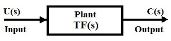
Figure 20.
Open-loop system block diagram.
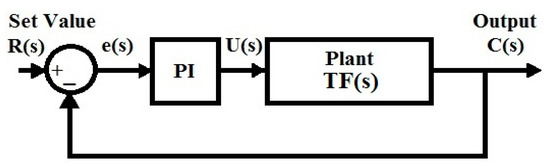
Figure 21.
Closed-loop system block diagram.
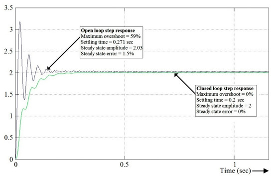
Figure 22.
Step response of the proposed converter for the open-loop and closed-loop systems.
4.2. The Closed-Loop Unidirectional Controller
The output voltage VO in this topology varied with the change in the input voltage sources V1 and V2. A PI controller was incorporated between the output and the input V2, as shown in Figure 23. The actual output voltage was compared with a set value or a reference voltage, and generated an error. The error was processed through a PI controller tuned with a proportional constant (KP) and an integral constant (KI). The output of the PI controller was again processed through a saturation block, the maximum limit of which was set to 0.8, so that the switch did not operate beyond an 80% duty cycle for the safety of the switch. The saturated signal then passed through a PWM block, which generated the switching pulses D2 for the voltage source V2. With the known values of V0, V1, V2, and D2, the switching pulses for V1, i.e., (D1) could then be found, using the output voltage equation of topology-1 (Equation (25)).
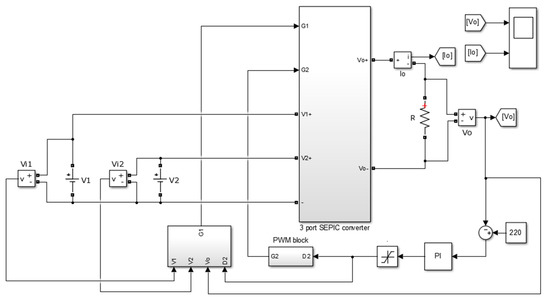
Figure 23.
Unidirectional closed-loop converter.
The reference value of the output voltage was set to be 220 V. With this closed-loop topology of a unidirectional structure, the output voltage was maintained at a constant value of 220 V, even if there was a variation in the input supply V1 and V2. The proportional gain constant (KP) of the PI controller was taken as 0.0001, and the integral gain constant (KI) was taken as 0.005. Figure 24 shows the output voltage and the output current of a unidirectional closed-loop converter.
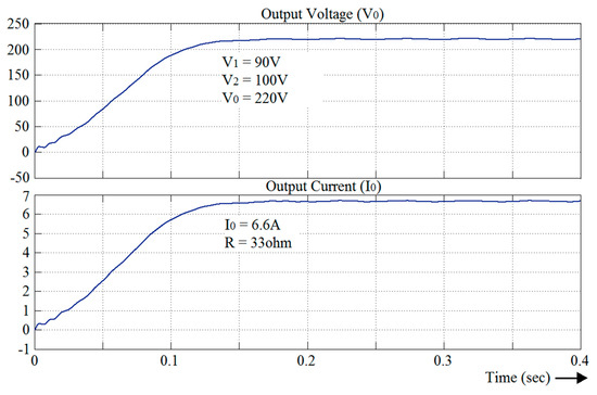
Figure 24.
Output voltage and current of a unidirectional closed-loop converter.
With 220 V as the reference voltage, the generated output was VO = 220 V with inputs V1 = 90 V and V2 = 100 V. From the results of the closed loop simulation, it was inferred that the output voltage of the converter remained constant with the variation of input source. The closed loop system reduced the steady state error and maximum overshoot to 0%.
4.3. The Closed-Loop Bidirectional Controller
In this design, as shown in Figure 25, two input voltage sources, a solar photovoltaic system and a battery were used. The output voltage VO varied with the variation of the input voltage sources. A PI controller was incorporated between the output and one of the input sources, depending on the availability of the sources. A P & O algorithm-based MPPT controller was incorporated with a PV input, in order to track the maximum available power. Three operating conditions were possible for this closed-loop structure.
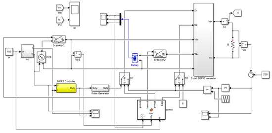
Figure 25.
Bidirectional closed-loop converter.
Case-1: When both sources supply to the load: When both the sources are active, then the MPPT controller generates the switching pulse (D1) for the cell containing the PV, and the PI controller generates the switching pulses (D2) for the cell containing the battery. The PI controller incorporated with the battery maintains the output voltage to the set value. The actual output voltage is compared with a set value or a reference voltage, and it generates an error. The error is processed through a PI controller tuned with a proper value of a proportional constant (KP) and an integral constant (KI). The output of the PI controller is again processed through a saturation block, the maximum limit of which is set to 0.8, so that the switch does not operate beyond the 80% duty cycle for the safety of the switch. The signal forms the saturation block that is fed to the pulse generation circuit or the PWM block, which generates the switching pulses D2 for the cell containing the battery source. Meanwhile, the MPPT controller transfers the maximum available power from the PV to the load.
Case-2: When sufficient solar power is available: When maximum solar power is available and it is sufficient to supply the load, then the MPPT controller has to be removed, and the PI controller will be incorporated between the load and the PV input. During this condition, if the battery is not fully charged, the switch for the battery port (S2) can be turned off. This makes the battery charge from the PV input. If the battery is fully charged, then it can be disconnected from the system through the breaker. The PI controller with the PV input will maintain a constant output, even if there is a variation in solar irradiation to an extent. The operating conditions for the above three cases are given in Table 5. The signals ‘pvcut’ and ‘batcut’ represent the operating signals for the breakers of the PV port and battery port, respectively. When ‘pvcut’ or ‘batcut’ is 1, then the corresponding breaker will be shorted, and the respective source will be added to in the system. Similarly, if it is 0, then the corresponding breaker will be open, and the respective source will be disconnected from the system. The signals ‘pvmpp’ and ‘batpi’ are the operating signals of the selection switches, allowing the switching of pulses to two respective switches, S1 and S2, of the input ports from the controllers. If ‘pvmpp’ is 1, then the switching pulse D1 will be generated from the MPPT controller, and if ‘pvmpp’ is 0, then the switching pulse D1 will be generated from the PI controller. Similarly, if ‘batpi’ is 1, then the switching pulse D2 will be generated from the PI controller, and if ‘batpi’ is 0, then the switching pulse D2 will be 0 and switch S2 turns off.
Table 5.
Control logic of a closed-loop bidirectional controller.
Case-3: When solar power is not available: When PV power is not available during the night or in cloudy weather, the battery alone will supply to the load, and maintain a constant output. During this condition, the PV can be disconnected from the system through a breaker. The PI controller is incorporated between the load and battery source. The actual output voltage is compared to the reference voltage, and it generates an error. The error is processed through the PI controller, tuned with a proper value of the proportional constant (KP) and the integral constant (KI). The output of the PI controller is again processed through a saturation block. The signal form the saturation block is fed to the pulse generation circuit or PWM block, which generates the switching pulses D2 for the cell containing the battery source.
In the output, the voltage shown in Figure 26 implies that it remains constant at a set value of 220 V, even if there is a variation in the PV input due to intermittent solar irradiation levels, to an extent. The proportional gain constant (KP) of the PI controller is taken as 0.0001, and the integral gain constant (KI) is taken as 0.005.
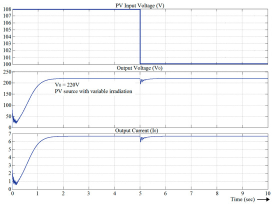
Figure 26.
PV input, output voltage, and current during intermittent solar irradiation.
Condition-1 of control logic: Figure 27 shows the output voltage and output current of a bidirectional closed loop converter when both the PV and the battery are supplying. The inputs are taken to be PV = 119 V, E = 120 V, and the initial battery state of charge is assumed to be 82%, as shown in Figure 28. From the results of the closed-loop simulation for this case, it is inferred that the output voltage of the converter remains constant at a set value of 220 V. Both sources are supplying to the load, and the battery is discharging.
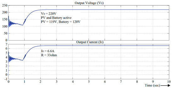
Figure 27.
Output voltage and current of a bidirectional closed-loop converter when both the PV and battery are supplying (condition-1 of control logic).
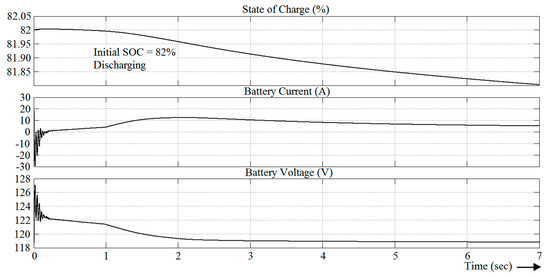
Figure 28.
SOC, current, and voltage of the battery during discharging (condition-1 of control logic).
Condition-2 of control logic: Figure 29 shows the output voltage and output current of a bidirectional closed loop converter when only the PV is supplying. The PV is taken to be PV = 123 V, and the initial battery state of charge is assumed to be 60%, as shown in Figure 30. The output voltage is maintained constant at a set value of 220 V, and the battery is charging.
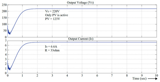
Figure 29.
Output voltage and current of a bidirectional closed-loop converter when only the PV is supplying (condition-2 of control logic).
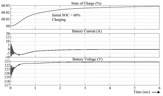
Figure 30.
SOC, current, and voltage of the battery during charging (condition-2 of control logic).
Condition-3 of control logic: In this case, if the battery is fully charged and PV is sufficient to supply the load, then the battery can be disconnected. For a fully charged battery, the initial battery SOC is assumed to be 99.9%. From the results of the closed-loop simulation for this case, in Figure 31 and Figure 32, it is inferred that the output voltage of the converter remains constant at a set value of 220 V. The PV is supplying to the load and the battery is disconnected.
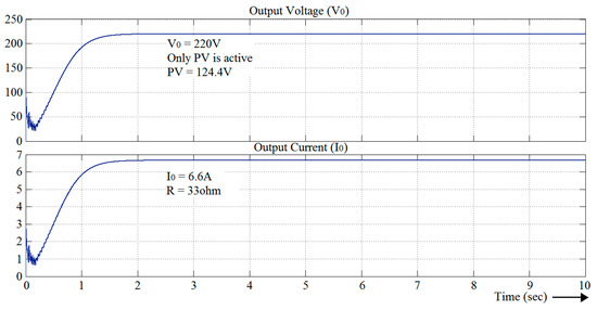
Figure 31.
Output voltage and current of a bidirectional closed-loop converter when only the solar PV is supplying, and the battery is fully charged (Condition-3 of control logic).
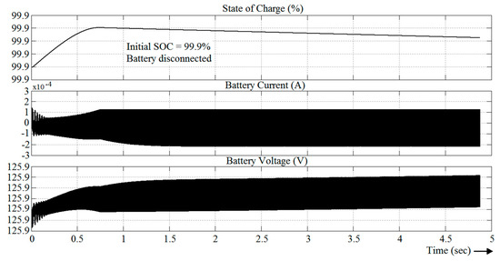
Figure 32.
SOC, current, and voltage of the battery when it is fully charged (Condition-3 of control logic).
Condition-4 of control logic: In this case, the solar PV supplies the load and charges the battery. The PV is taken to be PV = 119 V, and the battery is very much less charged. The initial battery state of charge is assumed to be 35%, as shown in Figure 33 and Figure 34. The output voltage is maintained constantly at a set value of 220 V, and the battery is charging.
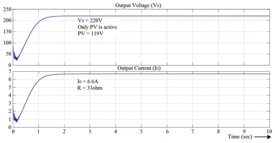
Figure 33.
Output voltage and current of a bidirectional closed-loop converter when only the solar PV is supplying, and the battery is undercharged (Condition-4 of control logic).
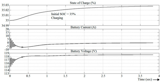
Figure 34.
SOC, current, and voltage of the battery when it is undercharged (Condition-4 of control logic).
Condition-5 of control logic: In this case, if the PV is not available or if irradiation level is 0, then the battery supplies to the load. The initial battery SOC is assumed to be 65%. From the results of the closed loop simulation for this case, in Figure 35 and Figure 36, it is inferred that the output voltage of the converter remains constant at a set value of 220 V. The PV is disconnected, and the battery supply to the load is being discharged.
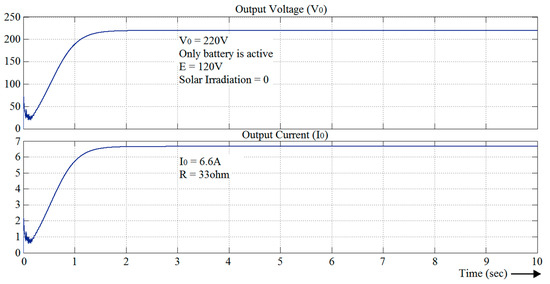
Figure 35.
Output voltage and current of a bidirectional closed-loop converter when only the battery is supplying (Condition-5 of control logic).
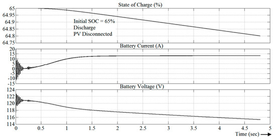
Figure 36.
SOC, current, and voltage of the battery (Condition-5 of control logic).
5. Experimental Verification
The simulation analysis of the open loop topology-1 was verified with a real-time hardware setup. The hardware setup was realized with two IGBTs (FGA15N120) and a high-frequency diode (HER3006PT). A DSPIC30F2010 microcontroller was used for generating the switching pulses. In both the input ports, V1 and V2, supply was provided by a solar PV system of equal power rating.
The input to PVSC1 is V1 = 35 V, whereas for PVSC2, V2 = 42 V. The duty cycle for two corresponding switches is: D1 = 67% and D2 = 50%. The components of the setup were designed to operate at a maximum of 1 kW. The component design parameters of the setup are given in Table 6.
Table 6.
Design parameters for the hardware setup.
With the given input and duty cycle, the calculated output voltage from Equation (26) was 81.66 V. The output of the MATLAB simulation of the proposed topology for the similar parameters was approximately 79 V. The output voltage of the proposed hardware setup for the given input and duty cycle was 78.8 V. This indicates that for similar values of parameters and inputs, the outputs corresponding to a mathematical analysis, MATLAB simulation, and hardware setup are approximately the same. Figure 37 shows the hardware setup of the three-port unidirectional topology.
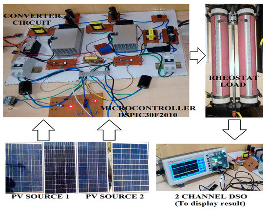
Figure 37.
Hardware setup of the proposed topology-1.
Figure 38a shows the input voltage waveform, V1 = 37 V and V2 = 42 V. Figure 38b shows the switching pulses of the switch S1 & S2, i.e., D1 = 67% and D2 = 50% respectively. Figure 39a shows the voltage across the switches. Figure 39b shows the current through the inductors. Figure 40a,b shows the voltage across the capacitors. Figure 41 shows the output voltage of the converter V0 = 78.8 V.
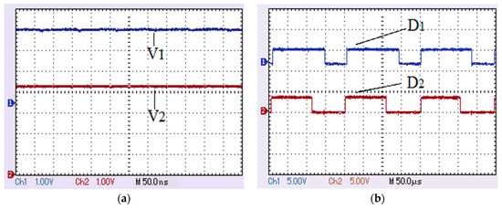
Figure 38.
(a) Input voltages (V1 = 35 V, V2 = 42 V), (b) switching pulses for S1 and S2 (D1 = 67% and D2 = 50%).
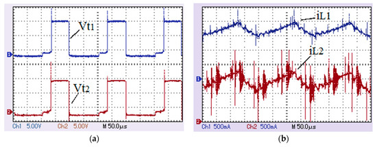
Figure 39.
(a) Voltages across switches S1 and S2 (Vt1 and Vt2), (b) currents through inductors L1 and L2 (iL1 and iL2).
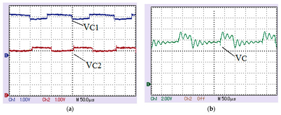
Figure 40.
(a) Voltages across the capacitors C1 and C2 (VC1 and VC2), (b) voltage across the output capacitor C (VC1).
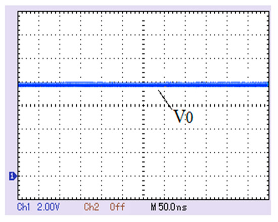
Figure 41.
Output voltage (V0 = 78.8 V).
6. Conclusions
In this paper, a unidirectional and bidirectional three-port converter based on SEPIC topology has been proposed and analyzed thoroughly. The detailed operations in various cases along with design concepts, theoretical analyses, have been cross verified through simulation and experimental results. The proposed three-port converter offers alternate solutions for integrating renewable sources with energy storage devices. This makes three port SEPIC-SEPIC converters a promising topology for electric vehicles, satellite, or DC micro-grid applications.
Author Contributions
Conceptualization done by C.A.; Supervision done by N.C., Methodology done by M.S.M.; Formal analysis done by S.V.
Funding
This research received no external funding.
Conflicts of Interest
The authors declare no conflict of interest.
References
- Liserre, M.; Sauter, T.; Hung, J. Future Energy Systems: Integrating Renewable Energy Sources into the Smart Power Grid through Industrial Electronics. IEEE Ind. Electron. Mag. 2010, 4, 18–37. [Google Scholar] [CrossRef]
- Carrasco, J.; Franquelo, L.G.; Bialasiewicz, J.; Galvan, E.; PortilloGuisado, R.; Prats, M.; Leon, J.I.; Moreno-Alfonso, N.; Prats, M.A.M. Power-Electronic Systems for the Grid Integration of Renewable Energy Sources: A Survey. IEEE Trans. Ind. Electron. 2006, 53, 1002–1016. [Google Scholar] [CrossRef]
- Wai, R.J.; Lin, C.Y.; Chen, B.H. High-Efficiency DC–DC Converter with Two Input Power Sources. IEEE Trans. Power Electron. 2012, 27, 1862–1875. [Google Scholar] [CrossRef]
- Shahzad, M.I.; Iqbal, S.; Taib, S. Interleaved LLC Converter with Cascaded Voltage Doubler Rectifiers for Deeply Depleted PEV Battery Charging. IEEE Trans. Transp. Electrif. 2018, 4, 89–98. [Google Scholar] [CrossRef]
- Wai, R.-J.; Duan, R.-Y.; Jheng, K.-H. High-efficiency bidirectional dc–dc converter with high-voltage gain. IET Power Electron. 2011, 5, 173–184. [Google Scholar] [CrossRef]
- Singh, A.K.; Pathak, M.K. Single-stage ZETA-SEPIC-based multifunctional integrated converter for plugin electric vehicles. IET Electr. Syst. Transp. 2017, 8, 101–111. [Google Scholar] [CrossRef]
- Lakshmi, M.; Hemamalini, S. Nonisolated High Gain DC–DC Converter for DC Microgrids. IEEE Trans. Ind. Electron. 2018, 65, 1205–1212. [Google Scholar] [CrossRef]
- Hwu, K.I.; Huang, K.W.; Tu, W.C. Step-up converter combining KY and buck-boost converters. Electron. Lett. 2011, 47, 722–724. [Google Scholar] [CrossRef]
- Lin, C.-C.; Yang, L.-S.; Wu, G.W. Study of a non-isolated bidirectional DC–DC converter. IET Power Electron. 2012, 6, 30–37. [Google Scholar] [CrossRef]
- Park, K.B.; Moon, G.W.; Youn, M.J. Nonisolated High Step-up Boost Converter Integrated with SEPIC Converter. IEEE Trans. Power Electron. 2010, 25, 2266–2275. [Google Scholar] [CrossRef]
- Wu, H.; Xu, P.; Hu, H.; Zhou, Z.; Xing, Y. Multiport Converters Based on Integration of Full-Bridge and Bidirectional DC–DC Topologies for Renewable Generation Systems. IEEE Trans. Ind. Electron. 2014, 61, 856–869. [Google Scholar] [CrossRef]
- Wu, H.; Zhang, J.; Xing, Y. A Family of Multiport Buck–Boost Converters Based on DC-Link-Inductors (DLIs). IEEE Trans. Power Electron. 2015, 30, 735–746. [Google Scholar] [CrossRef]
- Khaligh, A.; Cao, J.; Lee, Y.-J. A Multiple-Input DC–DC Converter Topology. IEEE Trans. Power Electron. 2009, 24, 862–868. [Google Scholar] [CrossRef]
- Li, Y.; Ruan, X.; Yang, D.; Liu, F.; Tse, C.K. Synthesis of Multiple-Input DC/DC Converters. IEEE Trans. Power Electron. 2010, 25, 2372–2385. [Google Scholar] [CrossRef]
- Wang, C.; Nehrir, M.H. Power Management of a Stand-Alone Wind/Photovoltaic/Fuel Cell Energy System. IEEE Trans. Energy Convers. 2008, 23, 957–967. [Google Scholar] [CrossRef]
- Veerachary, M. Two-Loop Controlled Buck–SEPIC Converter for Input Source Power Management. IEEE Trans. Ind. Electron. 2012, 59, 4075–4087. [Google Scholar] [CrossRef]
- Haghighian, S.K.; Tohidi, S.; Feyzi, M.R.; Sabahi, M. Design and analysis of a novel SEPIC-based multi-input DC/DC converter. IET Power Electron. 2017, 10, 1393–1402. [Google Scholar] [CrossRef]
- Patra, P.; Patra, A.; Misra, N. A Single-Inductor Multiple-Output Switcher with Simultaneous Buck, Boost, and Inverted Outputs. IEEE Trans. Power Electron. 2012, 27, 1936–1951. [Google Scholar] [CrossRef]
- Tummuru, N.R.; Mishra, M.K.; Srinivas, S. Dynamic Energy Management of Renewable Grid Integrated Hybrid Energy Storage System. IEEE Trans. Ind. Electron. 2015, 62, 7728–7737. [Google Scholar] [CrossRef]
- Rani, B.I.; Ilango, G.S.; Nagamani, C. Control Strategy for Power Flow Management in a PV System Supplying DC Loads. IEEE Trans. Ind. Electron. 2013, 60, 3185–3194. [Google Scholar] [CrossRef]
- McDonough, M. Integration of Inductively Coupled Power Transfer and Hybrid Energy Storage System: A Multiport Power Electronics Interface for Battery-Powered Electric Vehicles. IEEE Trans. Power Electron. 2015, 30, 6423–6433. [Google Scholar] [CrossRef]
- Tani, A.; Camara, M.B.; Dakyo, B. Energy Management Based on Frequency Approach for Hybrid Electric Vehicle Applications:Fuel-Cell/Lithium-Battery and Ultracapacitors. IEEE Trans. Veh. Technol. 2012, 61, 3375–3386. [Google Scholar] [CrossRef]
© 2019 by the authors. Licensee MDPI, Basel, Switzerland. This article is an open access article distributed under the terms and conditions of the Creative Commons Attribution (CC BY) license (http://creativecommons.org/licenses/by/4.0/).