Article

An Output Capacitor-Less Low-Dropout Regulator with 0–100 mA Wide Load Current Range

1
College of Information and Communication Engineering, Sungkyunkwan University, Suwon 16419, Korea
2
Samsung Electronics Co. Ltd., Hwaseong 18448, Korea
*
Authors to whom correspondence should be addressed.
Energies 2019, 12(2), 211; https://doi.org/10.3390/en12020211
Submission received: 23 November 2018 / Revised: 31 December 2018 / Accepted: 5 January 2019 / Published: 10 January 2019

Abstract

:
An output capacitor-less low-dropout (OCL-LDO) regulator with a wide range of load currents is proposed in this study. The structure of the proposed regulator is based on the flipped-voltage-follower LDO regulator. The feedback loop of the proposed regulator consists of two stages. The second stage is turned on or off depending on the variation in the output load current. Hence, the regulator can retain a phase margin at a wide range of load currents. The proposed regulator exhibits a better regulation performance compared to the ones in previous studies. The test chip is fabricated using a 65-nm CMOS process.

1. Introduction

Power management of mobile devices and communication networks have been advancing with the growing number of mobile consumer electronics and Internet of Things (IoT) devices. To improve their power efficiency and battery life, multiple levels of engineering efforts have been conducted from system-level optimization [1,2,3,4] to device-level power management such as dynamic voltage and frequency scaling [5,6,7,8]. Digital systems and system-on-chip devices usually have multiple voltage domains that need to be adjusted reflecting dynamic variations of load conditions. As a result, there is a great demand of power management integrated circuits (PMICs) with a high energy efficiency and accuracy across wide load ranges.
A PMIC takes battery power as input and provides clean power to core blocks such as an application processor (AP). Generally, core blocks require multiple levels of power, therefore, the PMICs contain several low-dropout (LDO) regulators to provide them. Because analog LDO regulators are generally targeted for sensitive circuits, it is important to attain a high power supply rejection (PSR) and fast response while maintaining a high energy efficiency and sound stability. A popular method of retaining the loop stability of an LDO regulator is by connecting a large off-chip capacitor to the output node. As PMICs contain a large number of LDO regulators, the loss of PCB area due to multiple off-chip capacitors cannot be ignored, particularly in mobile applications that require a small form factor. To overcome this problem, output capacitor-less LDO (OCL-LDO) regulators have been studied. One of the previous studies on the OCL-LDO regulator is an ultra-fast load-transient LDO regulator [9]. However, it uses a 600-pF decoupling capacitor, which consumes a large silicon area and may not be suitable for mobile PMICs. A full on-chip LDO regulator was introduced by Milliken et al., but it has a low loop gain resulting in a low power supply rejection ratio (PSRR) [10]. An ultra-low-power OCL-LDO regulator proposed in Reference [11] shows the best performance. However, its performance is susceptible to process variations. Flipped voltage follower (FVF) based LDO regulator designs have been developed [12,13,14,15]. A basic FVF-based LDO regulator has a simple folded structure, but it exhibits poor regulation characteristics [12,13]. In Reference [14], a dynamic biasing technique was acquired to improve the poor regulation characteristics, but its loop gain and PSR characteristics still required improvements. In Reference [15], the feedback loop of the LDO regulator has an additional second stage for a better PSR and regulation characteristics. However, it demands a minimum load current of 1–3 mA to maintain loop stability, thereby degrading the power efficiency under a light load condition. This study presents an FVF-based LDO regulator, which is stable even under a light load condition (0–1 mA).
This paper is organized as follows. The design challenges of conventional LDO regulators are described in Section 2. Section 3 presents the overall architecture of the proposed LDO with a detailed explanation of the implemented circuits. Section 4 shows the chip measurement results. Finally, Section 5 presents the conclusions.

2. Conventional LDO Regulators

2.1. Output Capacitor-Less LDO Regulator

Regulators can be classified as linear and switching regulators. Among these, linear regulators can supply clean power without noise, but they have a poor power efficiency due to a voltage drop (dropout voltage) in the variable resistor. The regulator structure that minimizes the dropout voltage is called an LDO regulator. Figure 1 shows the structure of a conventional LDO regulator. It takes input power at VIN and allows VOUT to provide clean output power. VOUT is designed to maintain a constant value through the negative feedback path consisting of an op-amp and a variable resistor RP. ROUT and CLOAD refer to the resistance and capacitance of the output stage, respectively. The variable resistor RP is implemented using a transistor called a power transistor. Because the feedback loop in Figure 1 is a system with at least two poles, frequency compensation is necessary for ensuring loop stability. In this case, a common method is to connect the output stage with the capacitor COUT that has a large value in μF, so that the pole of the output is always dominant. Although this method can easily perform frequency compensation, there exists the disadvantage of PCB area loss due to COUT. The LDO regulator introduced in Reference [9] succeeded in ensuring loop stability without external capacitors but used a 600-pF MIM capacitor to achieve a fast response. Although the PCB area was reduced successfully, a large amount of silicon area had to be used for the MIM capacitor, making it unsuitable for LDO regulators in mobile applications.

2.2. FVF-Based LDO Regulator

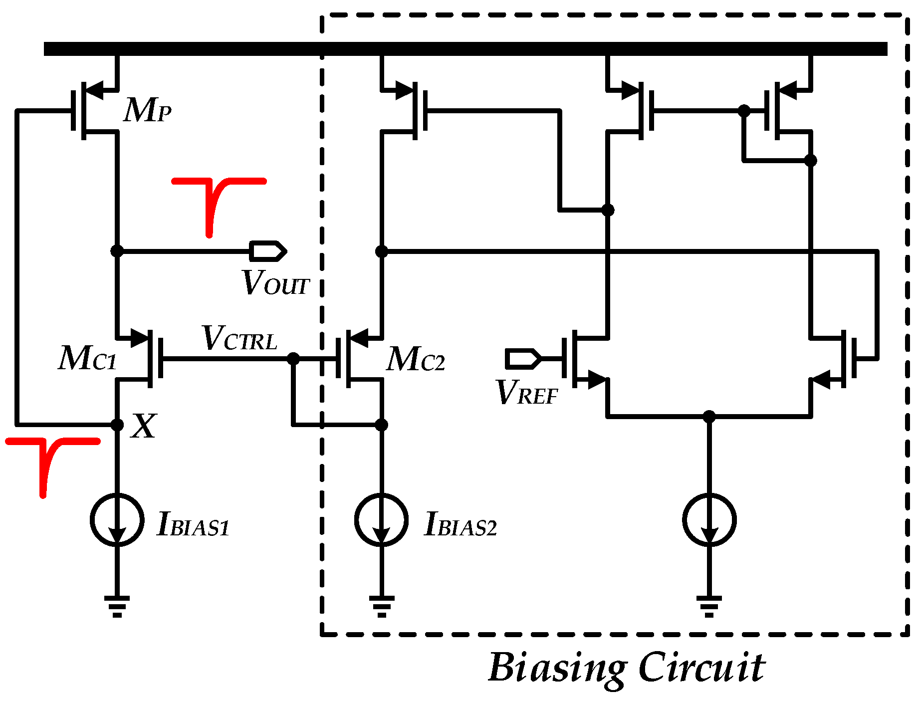
Figure 2 shows the basic structure of an FVF-based LDO regulator [12]. The regulator is composed of MP, the power transistor of the regulator, MC1, which senses the output voltage and adjusts the gate voltage of MP through the negative feedback, and IBIAS1, the current source. The biasing circuit on the right side determines VCTRL, the gate bias voltage of MC1. The source voltage of MC2 is fixed at VREF by the negative feedback of the biasing circuit. As MC1 and MC2 have the same bias current (IBIAS1 = IBIAS2) and aspect ratio, they have the same source voltage. Therefore, in the steady state, VOUT is determined as follows:
V O U T   =   V C T R L   +   V S G   ( o f   M C 1 )   =   V R E F
If output current increases abruptly, VOUT will decrease momentarily. MC1 will detect this variation of VOUT and the voltage at node X, which is the gate voltage of the power transistor MP, decreases accordingly. That is, the current flowing through MP will increase and recover VOUT to its initial level. In contrast, if the output current decreases rapidly, the gate voltage of MP will increase and restrain VOUT from increasing. The output load capacitance of the output capacitor-less LDO is primarily attributed to the parasitic capacitance of the power lines and it is typically less than 50 pF. Because the output impedance of the FVF-based LDO regulator is reduced drastically by the loop gain of the regulator feedback path, this feedback pushes the pole created at the output node away from a unit gain frequency of the regulator. As a result, the dominant pole is determined by the gate capacitance of the power transistor MP, not by the output load parasitic capacitor.

2.3. Voltage Spike Detection of FVF-Based LDO Regulator

A major disadvantage of the FVF-based LDO regulator is its poor load regulation characteristics. To overcome this, Milliken et al. [9] used a very large bias current (6 mA) to achieve the maximum bandwidth of the regulator. However, this technique is not applicable in mobile applications using limited battery power. Or et al. [14] proposed a dynamic bias method that drives the circuit with a minimum operating current with a maximum operating current only when a high driving current is required. The waveform of the relationship between output current and quiescent current is shown in Figure 3.
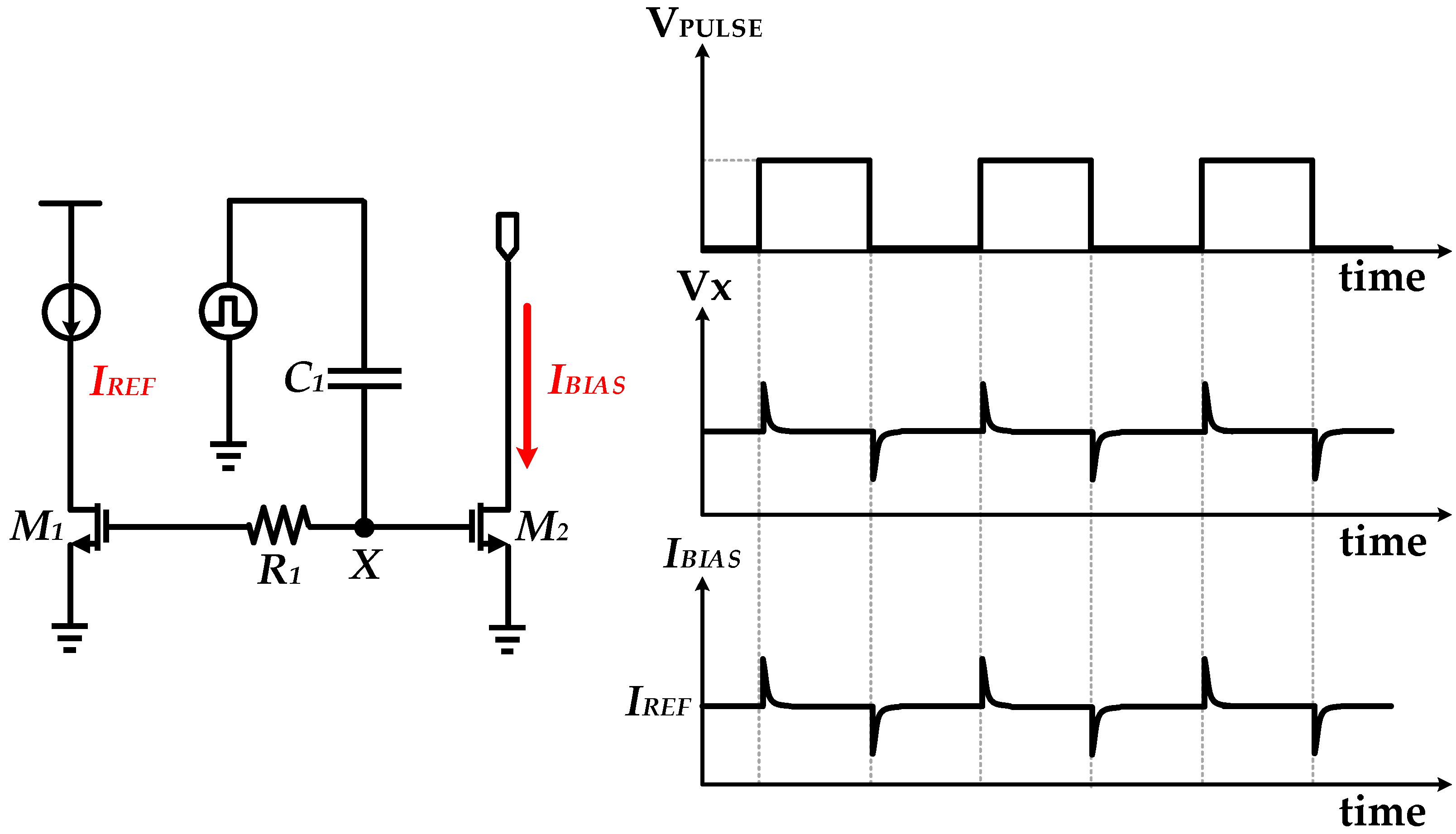
Figure 4 shows the structure and operating waveform of the voltage spike detecting current mirror [14]. A sudden change in the amount of current flowing through the output stage results in an abrupt change of the output voltage (emulated with a pulse voltage source in Figure 4). During this, only the high frequency component of the output voltage variation passes through C1 and affects node X leading to a rise in its voltage. Afterwards, the node X voltage is gradually recovered to the original value due to the R-C time constant of node X. Because the voltage at node X is the gate-source voltage of M2, the bias current (IBIAS) instantaneously increases, as shown in Figure 4 and then returns to its original value.
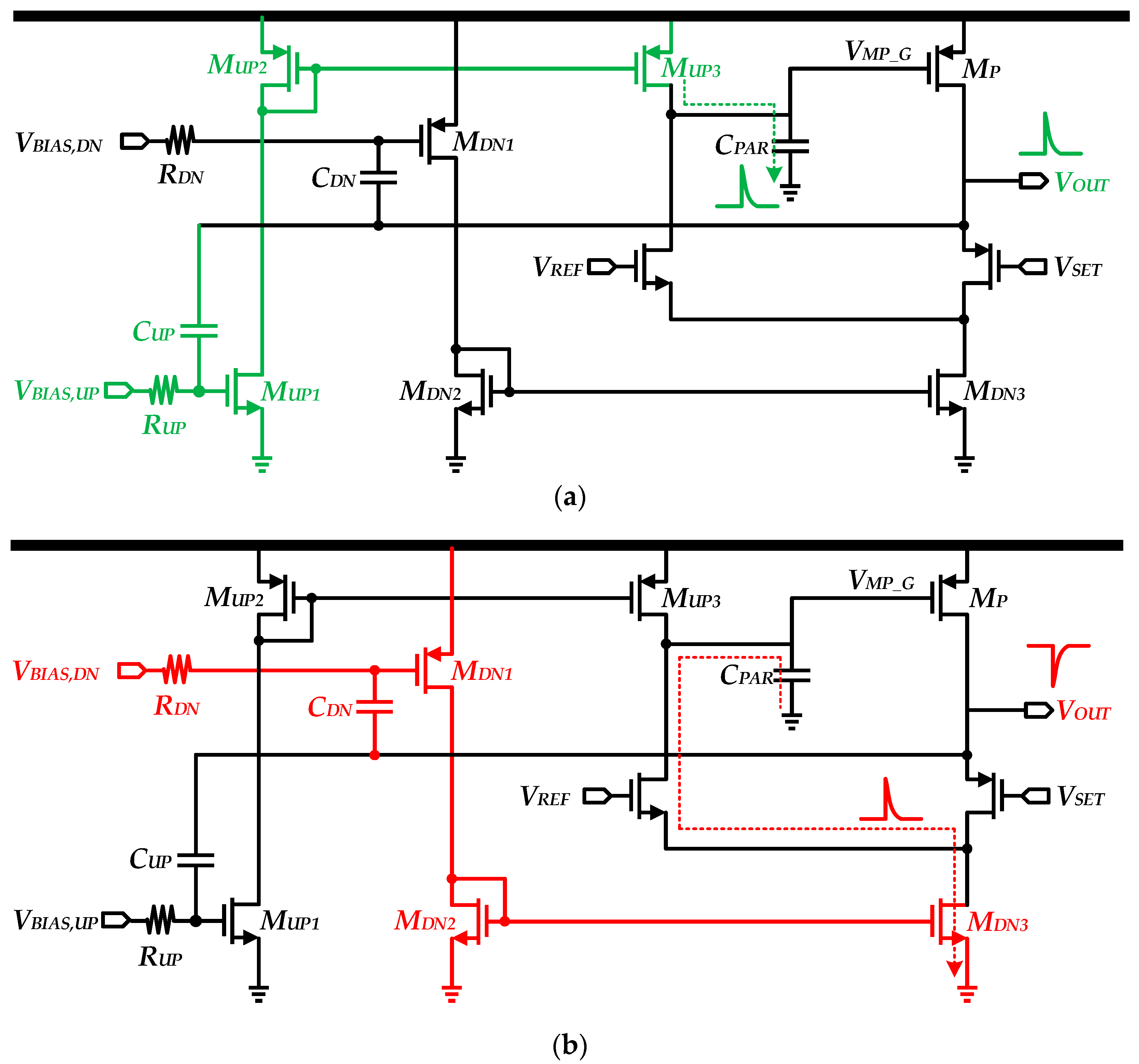
Figure 5 shows a structure that combines a FVF-based LDO regulator with a current mirror that detects voltage spikes. CPAR refers to the gate-stage parasitic capacitance of power transistor MP. To respond to abrupt voltage changes at the output stage, it is necessary to rapidly charge or discharge the CPAR. When a voltage overshoot occurs in the output stage, the CPAR can be charged quickly through the overshoot detection circuit consisting of MUP1,2,3, CUP, and RUP as shown in Figure 5a. Conversely, as shown in Figure 5b, when an undershoot occurs, the CPAR gets discharged fast through the MDN3 which is triggered by the undershoot detection circuit consisting of MDN1,2,3, CDN, and RDN. The bandwidth of the overshoot detection circuit can be adjusted by changing the RDN/UP and CDN/UP values. Owing to a fast loop response, this structure can respond faster to sudden VOUT changes than a conventional FVF-based LDO regulator. However, because the main loop of the regulator is composed of only one stage, the loop gain is too small to achieve a sufficient PSRR.

2.4. Loop-Gain-Enhanced FVF-Based LDO Regulator

Comparing to the conventional FVF-based LDO regulator, the circuit in Figure 6 has an additional stage to increase the loop gain. However, as the number of stages increases, the frequency compensation of the loop becomes complicated. Similar to the voltage spike detection regulator described earlier, this architecture also uses a dynamic bias current source. CM in Figure 6 serves as a Miller capacitor for frequency compensation and it detects the undershoot voltage at the output stage and discharges the gate capacitor of MP through MDISC. On the other hand, C1 senses the overshoot of VOUT and allows a large amount of current to flow to the gate capacitor of MP through MC. Adding this second stage increases the loop gain, which improves regulator performance such as the load and line regulation and PSRR. However, the disadvantage of this regulator is that a certain amount of output current must always flow through the output stage to ensure loop stability. According to a study [15], this minimum driving current should be at least a few milliamperes in a 90-nm process. As a result, although the regulation characteristics are improved through the loop gain enhancement and frequency compensation, the power efficiency in a low-power state still needs to be improved.

3. Proposed LDO Regulator

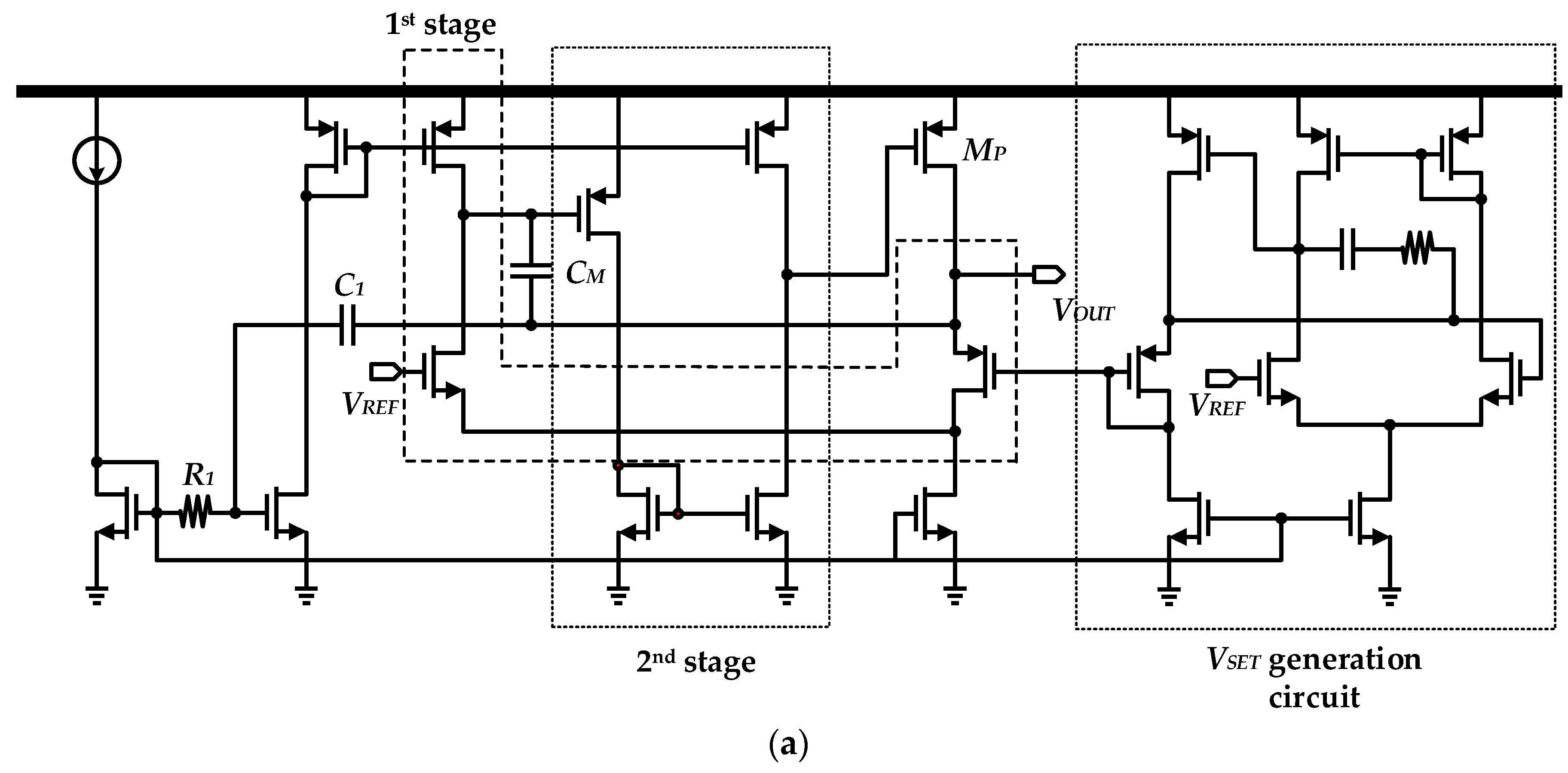
Figure 7a shows a full schematic representation of the enhanced loop gain FVF-based LDO regulator [15] originated from a basic FVF-based LDO regulator [12]. When compared with the basic regulator [12], the enhanced loop gain regulator has an additional second gain stage to boost the total loop gain of the regulator. However, this LDO regulator requires a certain amount of load current to achieve loop stability. If the regulator is under a light load condition, a complex pole is generated, degrading the stability of the loop and causing a long settling behavior.
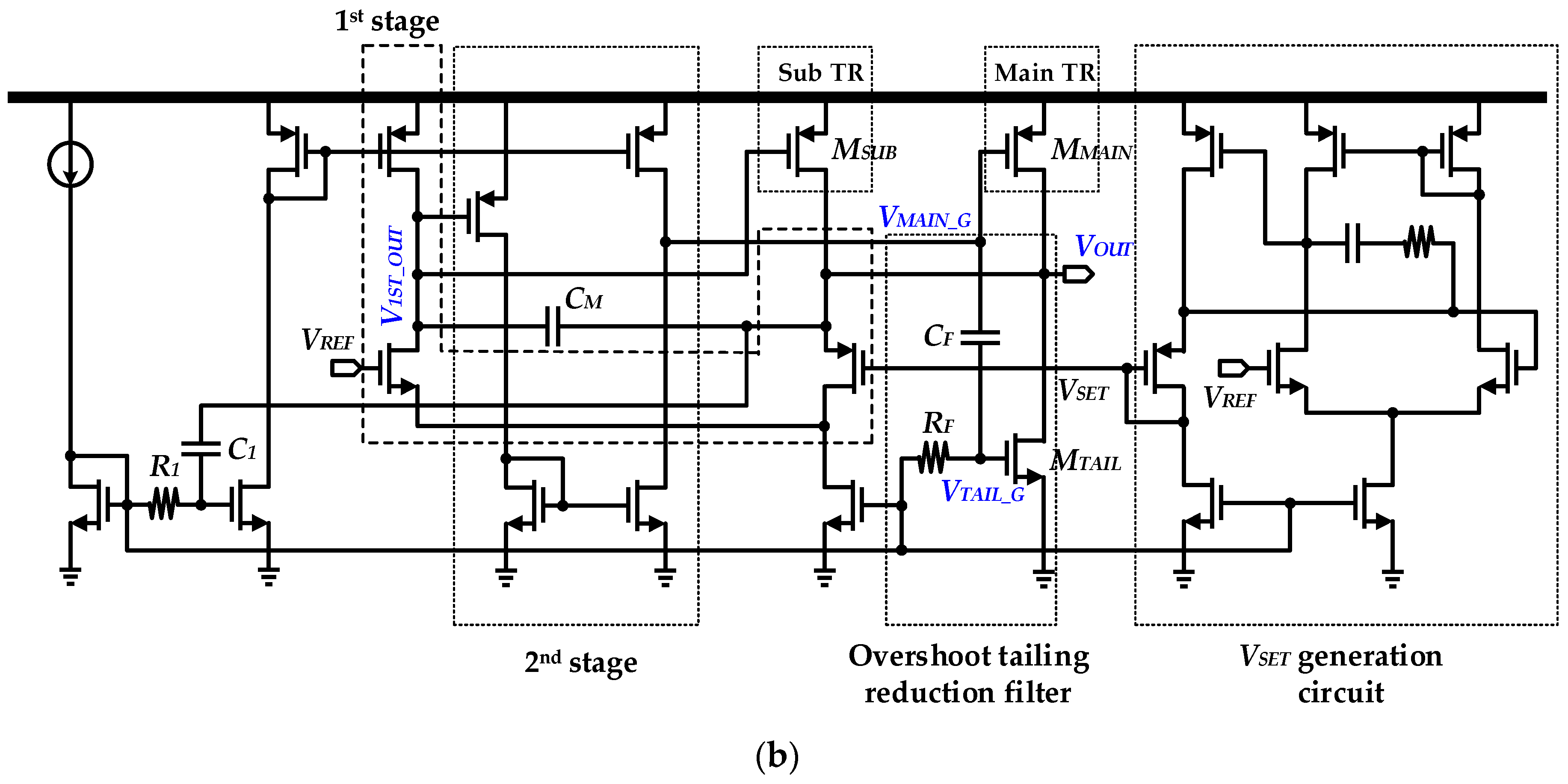
Figure 7b shows a full schematic representation of the proposed LDO regulator. The main idea of this regulator is that its operating mode is altered based on the level of the load current. If the load current is low, the regulator operates as a basic FVF-based LDO regulator [12]. However, if the load current is increased, the proposed regulator operates as an enhanced loop gain FVF-based LDO regulator [15]. As shown in Figure 7b, the proposed regulator mainly comprises a simple folded FVF as its first stage, a common-source structure as its second stage, a main power transistor (MMAIN), and a subsidiary power transistor (MSUB). In this circuit, the second stage and MMAIN are adaptively turned on or off depending on the output load current.
The operating mechanism of the proposed regulator is illustrated in Figure 8. Figure 8a shows the case where the load current reduces to less than 1 mA. It should be noted that this light load condition is not easily supported by the regulator in Reference [15]. In the proposed regulator, the gate voltage of MSUB is reduced by the first stage and MSUB is weakly turned on. MSUB is designed to have a small size (144 μm/0.06 μm), yet it can afford to drive the current under a light load condition. However, the second stage is almost turned off when the load current is extremely low. Even if the second stage is weakly turned on, the response of MMAIN is much slower than that of MSUB. In other words, when the regulator is under a light load condition, we can consider that only MSUB is turned on while the second stage and MMAIN are turned off. The proposed regulator operates like a basic FVF-based LDO regulator.
If the load current of the regulator is increased, the voltage level of node X (the gate of MSUB) is further reduced. Therefore, the second stage is turned on and it adds a considerable gain as M1 enters the saturation region. Under a heavy load condition, the first stage, second stage, MMAIN, and MSUB are fully turned on. However, the driving current of MSUB is one-tenth of that of MMAIN. Therefore, the effect of MSUB can be ignored as in Figure 8b. Consequently, under a heavy load condition, the proposed regulator operates as an enhanced loop gain FVF-based LDO regulator [15]. Moreover, it switches its operating mode depending on the amount of output load current. Hence, it can achieve stability even if the output load current is extremely low.
The proposed regulator is not a push-pull regulator. Therefore, it is difficult to recover the overshoot voltage at the output node. In this proposed circuit, an overshoot tailing reduction filter is introduced to prevent the output tailing voltage. The drain of MTAIL is connected to the output node and the gate voltage of MMAIN is filtered once and then connected to the gate node of MTAIL. When the output current is switched from a heavy to a light load, a high pass filter, which consists of RF and CF, detects the gate voltage of MMAIN and it momentarily increases the discharging current flowing through MTAIL. As a result, the output overshoot voltage is suppressed.
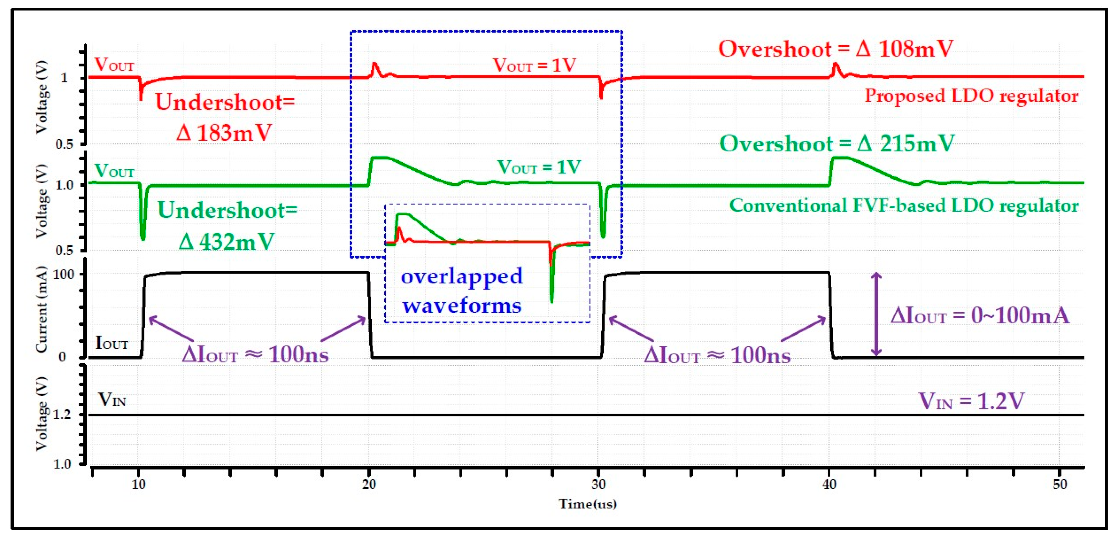
Figure 9 shows the simulated transient responses of the proposed and conventional FVF-based LDO regulators. The constant input voltage of 1.2 V is supplied and the load current is changed from 0 to 100 mA and vice versa. The rising and falling time of the load current is approximately 100 ns. Both LDO regulators have a constant output voltage of 1 V. The undershoot voltages of the proposed and conventional LDO regulators are 183 and 432 mV, respectively, and the overshoot voltages are 108 and 215 mV. We could confirm that the transient characteristics are significantly improved by the additional gain stage and the overshoot tailing reduction filter of the proposed LDO regulator.
Figure 10 and Figure 11 show how the internal nodes of the proposed and conventional FVF-based LDO regulators behave while the load conditions abruptly change. Figure 10a shows the simulated voltage waveforms of the two important nodes of a conventional FVF-based LDO regulator: VOUT (the output node of the LDO regulator) and VMP_G (the gate node of the power transistor, MP in Figure 5). When the load current is changed from 0 to 100 mA, VOUT drops first, but it is finally recovered to the initial voltage owing to the negative feedback circuit described in Figure 5. That is, VOUT rises again to the desired target as the gate voltage of the power transistor drops with approximately 487-ns delay. This delay is significantly shortened by inserting an additional stage in the proposed LDO regulator. Figure 10b shows the simulated waveforms of the proposed LDO regulator’s internal nodes: VOUT, V1ST_OUT (the output of the 1st stage), and VMAIN_G (the output of 2nd stage). When the load current is changed from light to heavy, V1ST_OUT and VMAIN_G ramps down approximately 1.8 times faster than VMP_G of the conventional FVF-based LDO regulator and achieving 1.8 times smaller undershoot.
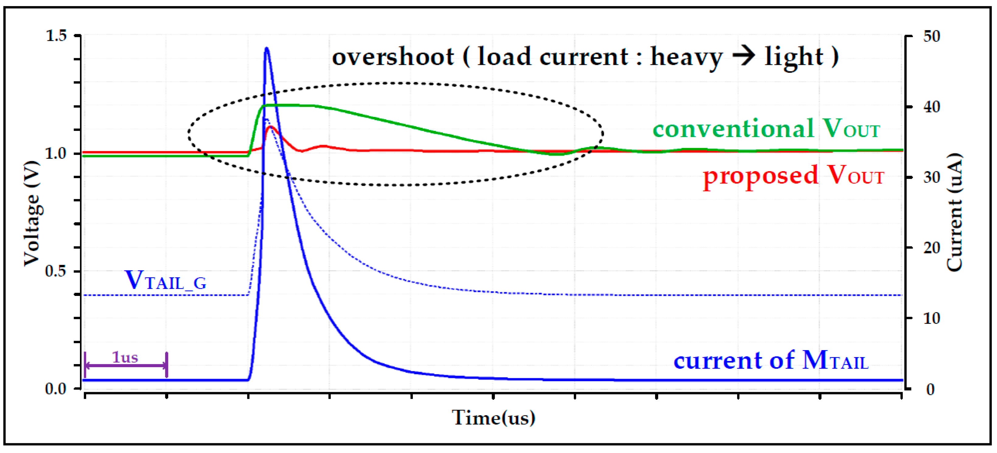
The simulation results in Figure 11 explain how the overshoot voltage is further suppressed by the overshoot tailing reduction filter. When the load current changes from 100 to 0 mA, VOUT is instantaneously increased. Almost simultaneously, VTAIL_G (the gate node of MTAIL in Figure 7b) also ramps up because of the coupling through the overshoot tailing filter and it momentarily increases the discharging current flowing through MTAIL. As a result, the output overshoot voltage is suppressed effectively and the duration of overshoot is reduced by approximately 3.5 times.

4. Measurement Results and Comparison

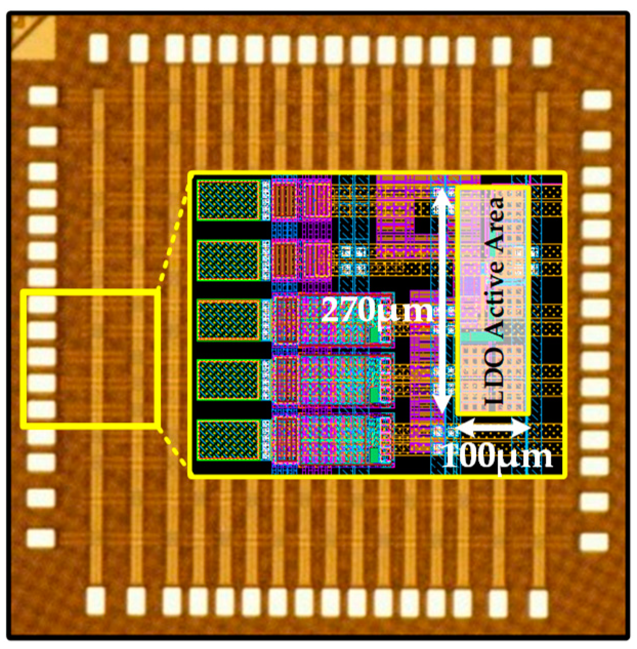
The proposed OCL-LDO regulator was fabricated using a 65-nm CMOS process. The chip micrograph is shown in Figure 12. Because of the metal filling in the process, it is difficult to distinguish the active area of the LDO in the micrograph. Therefore, we superimposed the layout with the micrograph. The LDO block occupies only 0.027 mm2 (270 μm × 100 μm). The additional blocks such as the 2nd gain stage and the overshoot tailing reduction filter occupy approximately 10% of the total area.
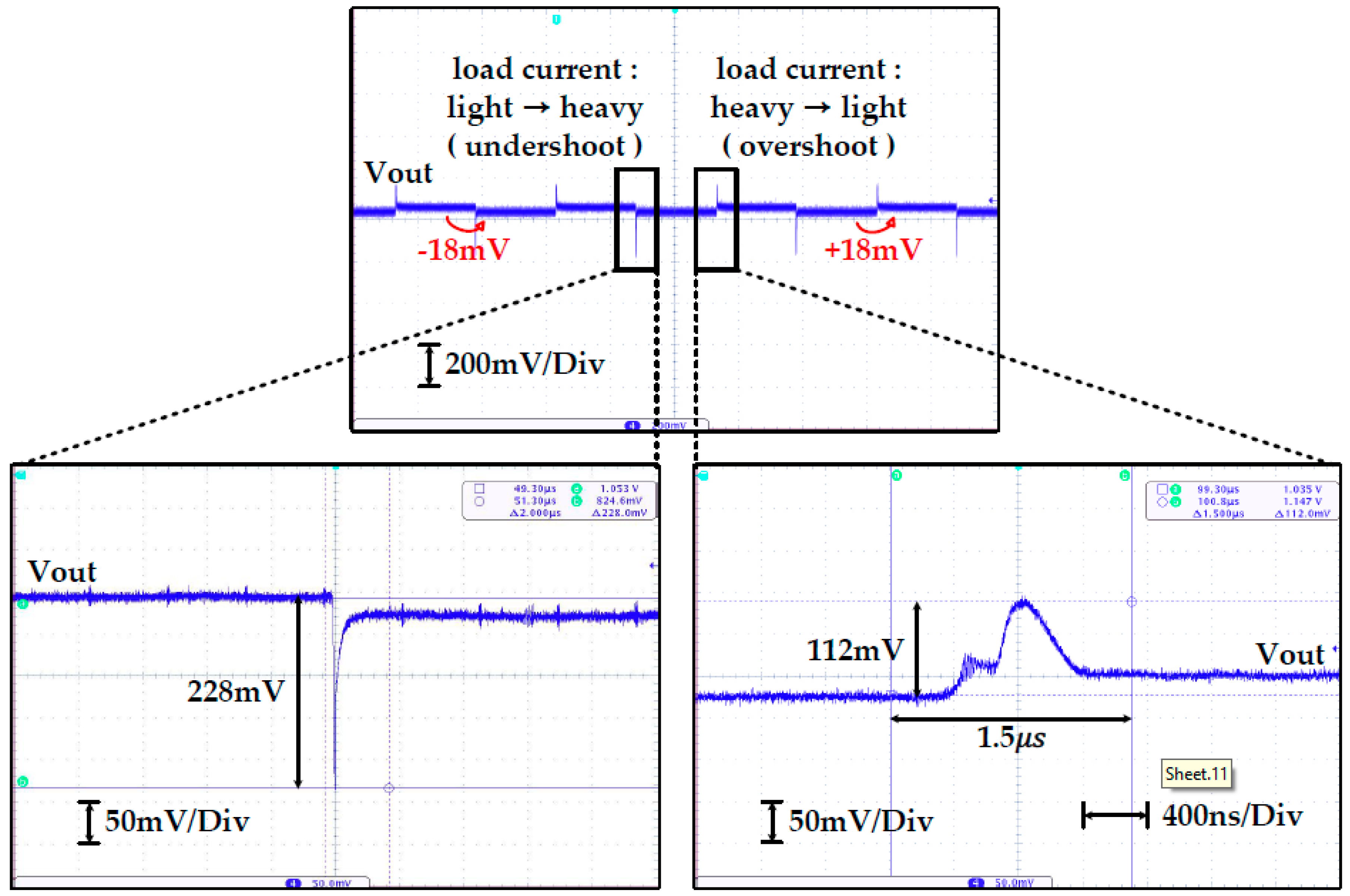
Figure 13 illustrates the measured load-transient responses. The waveform at the top shows the output voltage when the load current is changed from 0 to 100 mA and vice versa. The waveform at the bottom shows an enlarged image of the undershoot and overshoot that occur when the load current is changed from 0 to 100 mA and 100 to 0 mA, respectively. The target output voltage of the proposed LDO regulator is 1 V. The measured output voltage is 1 V ± 18 mV. The maximum undershoot and overshoot voltages are 228 and 112 mV, respectively. In [15], the overshoot time delay of the LDO regulator based on the enhanced loop gain is approximately 5 μs, whereas, in the proposed LDO regulator, the overshoot tailing reduction filter (Figure 7b) reduces the overshoot time delay to approximately 1.5 μs.
In Table 1, the performance of the proposed LDO regulator is compared with that of the previous capacitor-less LDO regulators. First, the proposed LDO has a wider range of load current, from 0 mA to 100 mA, whereas References [12,16] have a limited range of less than 50 mA and Reference [15] does not support ultra-light load conditions. The proposed LDO regulator is also competitive in terms of the quiescent current, response time, settling time, PSR, and load regulation capability.

5. Conclusions

We proposed a 65 nm CMOS OCL-LDO regulator, which is stable even under a light load condition. Under a heavy load condition, this regulator operates as an enhanced loop gain FVF-based LDO regulator. However, under the light load condition, the second stage is turned off and the proposed regulator operates as a basic FVF-based LDO regulator. As a result, the proposed regulator can achieve a full-range stability from 0 to 100 mA. Furthermore, the overshoot tailing reduction filter helps the regulator to achieve a better transient response. Compared to the previous literature, the proposed LDO regulator supports a wider range of load current and has a better transient regulation performance.

Author Contributions

J.P. and W.-J.K. proposed and designed the overall architecture of proposed output capacitor-less low-dropout (LDO) regulator. D.-S.K. contributed in test chip design and layout. J.P. performed experiments and evaluated results. Y.L. and J.-H.C. guided and directed the authors for this work.

Funding

This research was supported in part by the program for fostering next-generation researchers in engineering of National Research Foundation of Korea funded by the Ministry of Science and ICT (2017H1D8A2031628), and in part by the KIAT (Korea Institute for Advancement of Technology) grant funded by the Ministry of Trade Industry and Energy (No. N0001883, HRD Program for Intelligent Semiconductor Industry).

Conflicts of Interest

The authors declare no conflicts of interest.

References

  1. Tsiropoulou, E.E.; Katsinis, G.K.; Papavassiliou, S. Utility-based Power Control via Convex Pricing for the Uplink in CDMA Wireless Networks. In Proceedings of the 2010 European Wireless Conference (EW), Lucca, Italy, 12–15 April 2010. [Google Scholar]
  2. Tefek, U.; Lim, T.J. Clustering and Radio Resource Partitioning for Machine-Type Communications in Cellular Networks. In Proceedings of the 2016 IEEE Wireless Communications and Networking Conference, Doha, Qatar, 3–6 April 2016. [Google Scholar]
  3. Kastrinogiannis, T.; Tsiropoulou, E.E.; Papavassiliou, S. Utility-Based Uplink Power Control in CDMA Wireless Networks with Real-Time Services. In International Conference on Ad-Hoc Networks and Wireless; Springer: Berlin/Heidelberg, Germany, 2008; pp. 307–320. ISBN 978-3-540-85208-7. [Google Scholar]
  4. Tsai, Y.D.; Song, C.Y.; Hsieh, H.Y. Joint Optimization of Clustering and Scheduling for Machine-to-Machine Communications in Cellular Wireless Networks. In Proceedings of the 2015 IEEE 81st Vehicular Technology Conference (VTC Spring), Glasgow, UK, 11–14 May 2015. [Google Scholar]
  5. Kim, W.; Brooks, D.; Wei, G.Y. A Fully-Integrated 3-Level DC-DC Converter for Nanosecond-Scale DVFS. IEEE J. Solid-State Circuits 2012, 47, 206–219. [Google Scholar] [CrossRef]
  6. Lee, Y.H.; Chiu, C.C.; Peng, S.Y.; Chen, K.H.; Lin, Y.H.; Lee, C.C.; Huang, C.C.; Tsai, T.Y. A Near-Optimum Dynamic Voltage Scaling (DVS) in 65-nm Energy-Efficient Power Management With Frequency-Based Control (FBC) for SoC System. IEEE J. Solid-State Circuits 2012, 47, 2563–2575. [Google Scholar] [CrossRef]
  7. Lee, Y.H.; Peng, S.Y.; Chiu, C.C.; Wu, A.C.H.; Chen, K.H.; Lin, Y.H.; Wang, S.W.; Tsai, T.Y.; Huang, C.C.; Lee, C.C. A Low Quiescent Current Asynchronous Digital-LDO With PLL-Modulated Fast-DVS Power Management in 40 nm SoC for MIPS Performance Improvement. IEEE J. Solid-State Circuits 2013, 48, 1018–1030. [Google Scholar] [CrossRef]
  8. Kim, S.T.; Shih, Y.C.; Mazumdar, K.; Jain, R.; Ryan, J.F.; Tokunaga, C.; Augustine, C.; Kulkarni, J.P.; Ravichandran, K.; Tschanz, J.W.; et al. Enabling Wide Autonomous DVFS in a 22 nm Graphics Execution Core Using a Digitally Controlled Fully Integrated Voltage Regulator. IEEE J. Solid-State Circuits 2016, 51, 18–30. [Google Scholar] [CrossRef]
  9. Hazucha, P.; Karnik, T.; Bloechel, B.A.; Parsons, C.; Finan, D.; Borkar, S. Area-Efficient Linear Regulator With Ultra-Fast Load Regulation. IEEE J. Solid-State Circuits 2005, 40, 933–940. [Google Scholar] [CrossRef]
  10. Milliken, R.J.; Silva-Martinez, J.; Sanchez-Sinencio, E. Full On-Chip CMOS Low-Dropout Voltage Regulator. IEEE Trans. Circuits Syst. I 2007, 54, 1879–1890. [Google Scholar] [CrossRef] [Green Version]
  11. Chong, S.S.; Chan, P.K. A 0.9-μA Quiescent Current Output-Capacitorless LDO Regulator With Adaptive Power Transistors in 65-nm CMOS. IEEE Trans. Circuits Syst. I 2013, 60, 1072–1081. [Google Scholar] [CrossRef]
  12. Man, T.Y.; Leung, K.N.; Leung, C.Y.; Mok, P.K.T.; Chan, M. Development of Single-Transistor-Control LDO Based on Flipped Voltage Follower for SoC. IEEE Trans. Circuits Syst. I 2008, 55, 1392–1401. [Google Scholar] [CrossRef] [Green Version]
  13. Chen, H.; Leung, K.N. A Fast-Transient LDO Based on Buffered Flipped Voltage Follower. In Proceedings of the 2010 IEEE International Conference of Electron Devices and Solid-State Circuits (EDSSC), Hong Kong, China, 15–17 December 2010. [Google Scholar]
  14. Or, P.Y.; Leung, K.N. An Output-Capacitorless Low-Dropout Regulator With Direct Voltage-Spike Detection. IEEE J. Solid-State Circuits 2010, 45, 458–466. [Google Scholar] [CrossRef]
  15. Guo, J.; Leung, K.N. A 6-μW Chip-Area-Efficient Output-Capacitorless LDO in 90-nm CMOS Technology. IEEE J. Solid-State Circuits 2010, 45, 1896–1905. [Google Scholar] [CrossRef]
  16. Lu, Y.; Wang, Y.; Pan, Q.; Ki, W.-H.; Yue, C.P. A Fully-Integrated Low-Dropout Regulator With Full-Spectrum Power Supply Rejection. IEEE Trans. Circuits Syst. I 2015, 62, 707–716. [Google Scholar] [CrossRef]
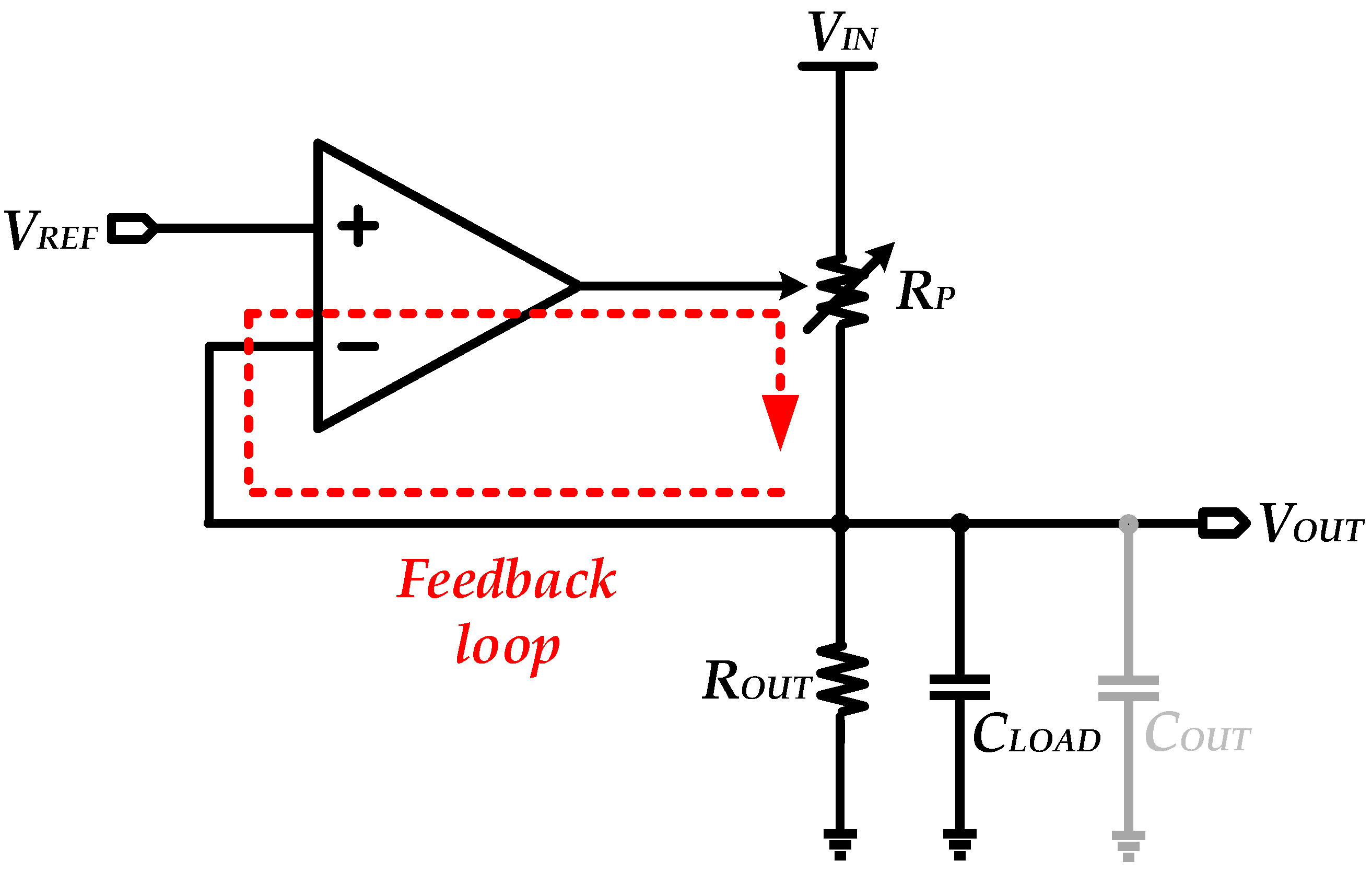
Figure 1. Conventional low-dropout (LDO) regulator.
Energies 12 00211 g001
Figure 2. Flipped voltage follower (FVF)-based LDO regulator [12].
Energies 12 00211 g002
Figure 3. Relationship between output current and quiescent current of an LDO regulator.
Energies 12 00211 g003
Figure 4. Operation principle of voltage spike detection circuit.
Energies 12 00211 g004
Figure 5. Operation principle of voltage spike detection FVF-based LDO regulator. (a) under overshoot condition; (b) under undershoot condition.
Energies 12 00211 g005
Figure 6. Structure of an LDO regulator based on a loop-gain-enhanced FVF [15].
Energies 12 00211 g006
Figure 7. Full schematic representations of LDO regulators: (a) loop gain enhanced FVF-based LDO regulator [15] and (b) proposed LDO regulator.
Energies 12 00211 g007aEnergies 12 00211 g007b
Figure 8. Operation principle of the proposed LDO. (a) with a light load current; (b) with a heavy load current.
Energies 12 00211 g008
Figure 9. Simulation results of transient responses with load current variations.
Energies 12 00211 g009
Figure 10. Simulation results of internal nodes’ transient responses: (a) conventional LDO regulator, (b) proposed LDO regulator and (c) comparison between conventional and proposed LDO regulators. (The load current is changed from 0 to 100 mA with 100-ns rising time).
Energies 12 00211 g010
Figure 11. Simulation results of the overshoot tailing reduction filter. (The load current is changed from 100 to 0 mA with 100-ns falling time).
Energies 12 00211 g011
Figure 12. Micrograph of proposed LDO regulator.
Energies 12 00211 g012
Figure 13. Measured load–transient response of the proposed LDO regulator with load current variation (0–100 mA).
Energies 12 00211 g013
Table 1. Performance comparison of capacitor-less LDOs.
ParametersTCAS-I 2008 [12]JSSC 2010 [15]TCAS-I 2015 [16]This Work
Process [nm]350906565
LDO TypeAnalogAnalogAnalogAnalog
Input Voltage [V]1.20.75–1.21.21.2
Output Voltage [V]10.5–111
Load Current Range [mA]0–503–1000–100–100
Max Load Current, IMAX [mA]5010010100
Quiescent Current, IQ [μA]95850–9030
Peak Current Efficiency [%]99.8199.99n/a99.97
PSR [dB] @ 10 MHzn/a25 @ 10 kHz<2026
∆V [mV] @ Load Step [mA]164 @ 50114 @ 9782 @ 10228 @ 100
Response Time, TR [ns] 13.280.0571.150.228
Settling Time [ns]<3005000>100<2000
Load Regulation [mV/mA]0.280.11.10.18
Total On-chip Capacitor [nF]Not requiredNot required0.14Not required
Active Area [mm2]0.04480.0190.0230.027
FOM1 [ps] 26.2320.0055.740.068
1TR = COUT × ΔV/IMAX [9]; 2 FOM1 = TR × IQ/IMAX [9].