Abstract
With the increasing demand for electric vehicles, the requirements of the market are changing ever faster. Therefore, there is a need to improve the electric car’s design time, where simulations could be an appropriate tool for this task. In this paper, the modeling and simulation of an inverter for an electric vehicle are presented. Four different modeling approaches are proposed, depending on the required simulation speed and accuracy in each case. In addition, these models can provide up to 150 different electric modeling and three different thermal modeling variants. Therefore, in total, there were 450 different electrical and thermal variants. These variants are easily selectable and usable and offer different options to calculate the electrical parameters of the inverter. Finally, the speed and accuracy of the different models were compared and the obtained results presented.
1. Introduction
The electric vehicle market has grown rapidly worldwide in the last few years. The growth of sales in electric vehicles (EV) is projected to continue due to decreasing battery prices, increasing environmental awareness among customers, and decreasing charging time [1]. A total of 1.1 million EV were sold worldwide in 2017, while the prevision for 2025 is around 11 million vehicles [2]. Electric vehicle ownership will increase to about 125 million by 2030 [3].
The necessities of the market will change faster and faster, so EV manufacturers will need to adapt to these changes. Production periods will need to be shorter, and in order to improve the design time, simulations can be a suitable tool. However, simulating the behavior of an EV for a long time may be a slow process as these simulations are based on electronic and thermal circuits. Simulating power electronics parts can consume a lot of time, but is critical to determine the electro-thermal performance inside the EV [4,5].
The solution could be to simplify models in order to enhance simulation times, but it must be considered that there will probably be a loss of accuracy in the results. Therefore, it is necessary to obtain different detailed models for different EV situations, and to evaluate the behavior as a trade-off between accuracy and speed.
Figure 1 presents the power train scheme of an EV. It is composed of different elements such as the battery, DC/DC converters, DC/AC inverter, etc., which are essential for the correct operation of the EV.
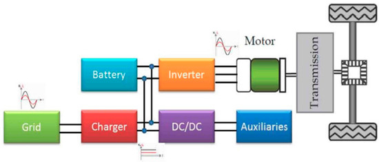
Figure 1.
Electric car power train scheme [6].
In this paper, the EV inverter was modeled and analyzed where the inverter was a two level three-phase converter (2L-VSC). It must be remarked that the models can be adapted to other configurations of inverters with minimum changes. In Figure 2, the structure of a classical two level three-phase inverter is presented.
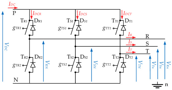
Figure 2.
Two level three-phase inverter comprising the DC link (with VDC, IDC voltage, and current highlighted), six bidirectional switches (six active switches and six antiparallel diodes), and the output phase terminals (with phase current and voltages IRST, VRST-N, VRST-n, highlighted).
The core of the inverter was the different semiconductors models, which were combined to build the inverter model. This model was divided into two main parts: the electric part and the thermal part. Both parts were joined through the electric model concerning power losses and the junction temperature of the semiconductors, as can be seen in Figure 3.
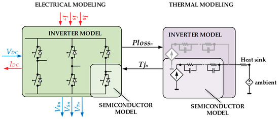
Figure 3.
Electro-thermal model coupling represented by the electrical and thermal model. VDC and IDC are the DC bus voltage and current, VRn, VSn, and VTn and IR, IS and IT are the AC side voltages and currents, Plossn and Tjn are the semiconductors (diodes and switches) power losses and junction temperature, respectively.
The published literature on EV inverters has been more related to design/topology analysis than the modeling issues. Furthermore, these publications are usually focused on a single semiconductor technology such as classical silicon [7,8] or novel wide band gap devices as silicon carbide [9,10]. However, for a performance and behavioral comparison, a universal model—where different semiconductor technologies can be interchangeable—is mandatory.
When developing a model, there is a long distance between academia (universities) and the final customers (generally original equipment manufacturers, OEMs). On one hand, academia and universities always try to develop very accurate inverter models. These heavy models can have a high time consumption and are difficult to parametrize, especially for a non-expert final user. On the other hand, final customers, especially OEMs, need fast and “light” models that can be parametrized and used by final non “inverter expert” users.
The usefulness of different accuracy/speed level models could go from the simulation of the energy consumption of an EV during one day of the worldwide harmonized light vehicle test procedure (WLTP) driving cycle, where a high-speed model is necessary, or the analysis of the inverter diode under a regenerative braking situation, where a high accuracy model is necessary.
The main objective of this paper is to shorten the gap between academia and OEMs by developing different accuracy models. The simulation of a short circuit in an inverter leg, or the simulation of an EV energy optimization routine of several days does not require the same accuracy and simulation speed. The detailed simplification of the models presented in this paper will help the final user decide which model is the most suitable for the final simulation objective.
2. Semiconductor Modeling
The power semiconductors are the main component of the inverter. A semiconductor allows for the electrical current conduction to be controlled, and the distribution of the semiconductors in the proper way makes it possible to build a controlled voltage source capable to control any load such as an electric motor. Although the schematic of the three phase-2L-VSC in Figure 2 represents them as ideal (bidirectional conduction, null voltage drop, instantaneous commutation), state-of-the-art semiconductors are still far for being considered ideal [11,12,13,14,15,16].
The semiconductors modeled in this paper considered four physical phenomena:
- Conduction voltage drop
- Conduction power losses
- Switching power losses
- Thermal behavior (as described in Section 4)
The following sections describe the different approaches in modeling the first three electrical phenomena.
2.1. Conduction Voltage Drop Variants
The conduction behavior of any semiconductor is usually modeled by the combination of a threshold voltage drop (Vth) and an on-resistance (Ron) (Figure 4) [17]. Considering a non-ideal semiconductor-based inverter leg, the total voltage drop between the two terminals of a semiconductor means a slight reduction or deviation from the theoretical obtainable output voltage. This can become an important factor when modeling an inverter in voltage sensitive applications such as the series connection of semiconductor devices, low voltage electric vehicle drives, and high-speed flux weakening control.
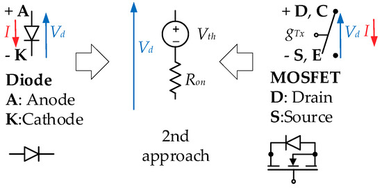
Figure 4.
Analysis of implementation of the second approach in a diode and a MOSFET configuration.
Five different variants have been developed to calculate the inverter’s conduction voltage drop (Figure 5): the ideal output voltage; on-resistance (Ron) and threshold voltage (Vth) dependent voltage drop; junction temperature (Tj) dependent voltage drop; current dependent voltage drop; and current and Tj dependent voltage drop.
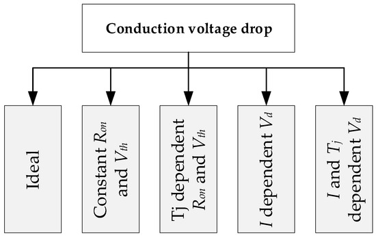
Figure 5.
The considered five conduction voltage drop calculation variants.
2.1.1. Ideal Output Voltage
With this variant, the semiconductors’ voltage drops are neglected and the voltage at output is considered ideal. The phase to the negative of the DC source output voltage (Vph-N) of the inverter will be calculated as follows in Equations (1) and (2):
where gT refers to the set of gate logic signals that control the state of each leg/half-bridge of the inverter and VDC is the DC bus voltage.
2.1.2. Ron and Vth Dependent Voltage Drop
In this variant, each semiconductor is modeled as a set of a threshold voltage drop (Vth) and an on-resistance (Ron), according to their forward conduction curves, where both are considered constant. For that purpose, an average value was chosen for each of them as in Equations (3) and (4). In this case, the junction temperature does not affect to the output voltage value.
where I is the conducted current.
2.1.3. Tj Dependent Voltage Drop
In this case, the Ron and the Vth that model the conduction of the semiconductors are junction temperature dependent (Equations (5) and (6)).
where Ron(Tj) refers to the junction temperature-dependent internal resistance of the semiconductor and Vth(Tj) is the junction temperature dependent-voltage threshold.
2.1.4. Current Dependent Voltage Drop
In this variant, the voltage drop produced during conduction (Vd) is modeled by means of a lookup table dependent on conducted current, according to the forward characteristic of each semiconductor (Equation (7)). Thus, this variant does not consider the dependence on junction temperature.
where Vd,1D-LUT (I) is the conducted current-dependent voltage drop in the semiconductor.
2.1.5. Current and Tj Dependent Output Voltage
In this case, the junction temperature is also considered for the forward characteristics (Equation (8)). The voltage drop will be calculated using two-dimension lookup tables.
where Vd,2D-LUT (I,Tj) is the conducted current and junction temperature dependent voltage drop in the semiconductor.
2.2. Conduction Losses
In order to increase the simulation speed, the universal losses model was chosen to calculate the power losses [18]. The universal losses model separates the conduction behavior and the switching behavior of the semiconductor. As described in [18], the universal losses model has been proven to be a good solution to achieve a good compromise between accuracy and computational cost.
The objective of the developed power loss model was to analyze the semiconductor as electrically-ideal (see Figure 6), and to calculate the power losses in a parallel way.
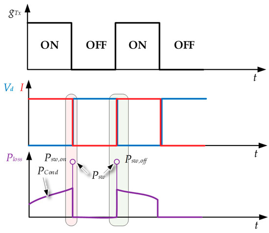
Figure 6.
Electric behavior modeling, ideal conduction and switching waveforms and conduction and switching losses estimation [19].
Regarding the conduction losses, when a semiconductor is turned on, it behaves as an ideally gate controlled (gT) switch, which results in a voltage drop Vd through its terminals, as described in Section 2.1. Depending on the required model accuracy, the voltage drop can be modeled taking into account different variables. The antiparallel diode can also be modeled through the same approach. The ideal switching waveforms of a semiconductor and its power losses (conduction and switching) can be seen in Figure 6.
The conduction losses are directly related to the voltage drop, as the power loss produced during the on-state is equal to the product of the voltage drop and the conducted current (Equation (9)).
Therefore, according to the five different variants modeled for the conduction behavior, the conduction losses can be modeled by means of their equivalent voltage drop models (Figure 7).
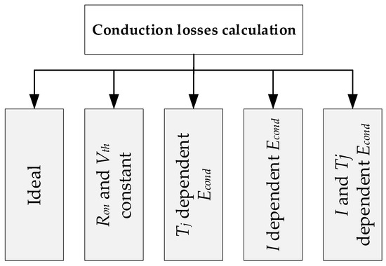
Figure 7.
The considered five conduction power losses calculation variants.
2.2.1. Ideal Conduction
In this case, the conduction of the semiconductor is considered ideal, so the conduction losses will be zero (Equation (10)).
2.2.2. Constant Ron and Vth Conduction Losses
In this variant, like in the Ron and Vth dependent output voltage calculation, each semiconductor is modeled as a set of a voltage drop (Vth) and an on-resistance (Ron), according to their forward conduction curves, where both are considered constant (Equation (11)). An average value is chosen and the junction temperature is not taken into account.
2.2.3. Tj Dependent Conduction Losses
The difference with the previous variant is that the Ron and Vth parameters are not constant, but dependent on the junction temperature. The conduction losses are calculated as follows (Equation (12)):
2.2.4. Current Dependent Conduction Losses
In this variant, as is done in the conduction voltage drop calculation, Vd is modeled by means of a lookup table dependent on the conducted current, according to the forward characteristic of each semiconductor. This variant does not consider the dependence on junction temperature. Therefore, the conduction losses are calculated by multiplying the voltage drop and the current (Equation (13)).
2.2.5. Current and Tj Dependent Conduction Losses
The difference between this variant and the previous is that in this case, the voltage drop is dependent on the current and the junction temperature (Equation (14)).
2.3. Switching Losses
Like the conduction power losses, the switching losses are calculated by means of the universal losses model [18,19,20,21]. The switching losses appear during the turn-on and turn-off transition of the semiconductors. The universal losses model considers those commutations as ideal transitions, that is, considering instantaneous commutations and ignoring the transient overvoltage, as can be seen in Figure 6. The power losses produced in each transition are added afterward as instantaneous energy losses (Esw,on, Esw,off), distributed along a switching step time (Equation (15), Figure 6).
where represents the simulation step size.
Therefore, while the waveforms are considered ideal in any modeling scenario, the switching power losses are approached by means of six different variants (Figure 8).
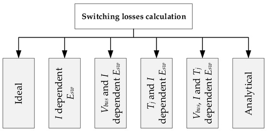
Figure 8.
The considered six switching power losses calculation variants.
2.3.1. Ideal Switching
This variant neglects the switching power losses of the semiconductors (Equation (16)).
2.3.2. Current Dependent Switching Losses
In this case, switching losses are calculated only taking into account the current. Depending on the conducted current and considering the datasheet or specific pulse tests performed to the semiconductors, the switching (on and off) energy losses can be obtained using a 1D-LUT (Equations (17) and (18)). The switching power losses depend on those energy losses and the simulation step.
where Esw,on,1D-LUT (I) and Esw,off,1D-LUT (I) refer to the current-dependent switching energy losses in a semiconductor.
2.3.3. Voltage and Current Dependent Switching Losses
In this case, the energy losses are dependent on the conducted current and the blocking voltage in each semiconductor (V) in a 2D-LUT. The switching losses are calculated as follows:
where Esw,on,2D-LUT (I,V) and Esw,off,2D-LUT (I,V) refer to the current and voltage dependent energy losses in a semiconductor.
2.3.4. Tj and Current Dependent Switching Losses
In this case, the energy losses are calculated taking into account the conducted current and the instantaneous junction temperature (Equations (21) and (22)).
where Esw,on,2D-LUT (I,Tj) and Esw,off,2D-LUT (I,Tj) refer to the current and junction temperature dependent energy losses.
2.3.5. Voltage, Tj and Current Dependent Switching Losses
The most detailed way to obtain the switching power losses consists in taking into account the conducted current, the blocking voltage, and the junction temperature (Equations (23) and (24)).
where Esw,on,3D-LUT (I,V,Tj) and Esw,off,3D-LUT (I,V,Tj) refer to the current, voltage, and junction temperature dependent energy losses.
2.3.6. Analytical Switching Losses
This variant calculates the switching losses analytically according to (Equations (25) and (26)). In order to achieve these analytical calculations, it is necessary to know the turn on and turn off times of the semiconductor. This data can be obtained from datasheet, gate resistor design process, or through experimental tests. The energy loss involved in each commutation responds to the integral of the voltage and current coexistence period.
where ton is the turn on time and toff is the turn off time of the semiconductor.
2.4. Blocking Behavior
Apart from the previously described physical phenomena, a fourth electrical phenomenon has been modeled in some of the analyzed scenarios. The models that are based on modeling physical semiconductors require modeling, even the blocking state (off state) with a current and voltage relationship. The blocking behavior of the semiconductors was considered negligible in this project, thus a highly resistive (above mega ohms) constant blocking resistance (Roff) was introduced to comply with this required relationship to run the simulations. The possible resultant blocking losses were neglected. However, in some applications such as battery powered portable devices, the blocking behavior could be linked to a standby consumption, and could be crucial for the application.
3. Inverter Electrical Models
The electrical model of the 2L-VSC inverter was built by combining the different electrical models of the semiconductors explained in Section 2 [21,22,23,24].
In some cases, an inverter model user will need an accurate and specific model to simulate the most detailed electric phenomena such as short circuits and other failure situations. For that kind of simulation, models of the highest fidelity have been developed by means of a high detail electric simulator, hereinafter called the high fidelity model (Hi-Fi).
As the higher accuracy involves a higher computational cost, second fidelity level models have been developed, with a lower accuracy, hereinafter called the medium fidelity model (M-Fi). The M-Fi model is based on an equation based simulator and provides a considerable simulation time reduction with a minimum accuracy loss.
The low fidelity model (Lo-Fi) represents a third fidelity level, which requires less computational cost than their equivalent Hi-Fi and M-Fi models. The Lo-Fi model is also an equation-based simulator model, but unlike the M-Fi model, this model only considers the generation of the fundamental harmonic of the output voltage, increases the simulation step size up to the switching period, neglects the commutations of the semiconductors, and thus notoriously improving the computational cost and simulation speed.
The simulation step size of the Lo-Fi model can be increased to several switching periods, in order to be able to run simulations of minutes or several hours in a relatively short time and with a reduced accuracy loss, with the so called fast low fidelity (Fast Lo-Fi) model.
Figure 9 shows a general scheme of the developed inverter models, where only the electric phenomena are reflected. Figure 9 represents the hierarchy workflow diagram of the developed models. The models are distributed inversely by their computational cost (simulation speed) and their similarity to a real converter (accuracy).
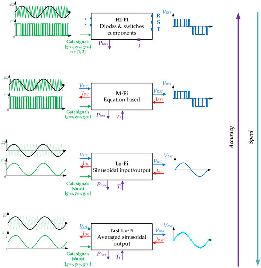
Figure 9.
Model simplification resume scheme, presented in order of decreasing accuracy and increasing speed. Four different models have been developed.
In that electric model scheme, the input/output connections and signals, the thermal variables and the control variables of each model can be identified. Figure 9 shows that the Fast low fidelity model was the model with the lowest computational cost, but was less accurate, while the high fidelity model provides just the opposite performance in terms of computational cost and accuracy.
The developed Hi-Fi, M-Fi, Lo-Fi, and Fast Lo-Fi models are explained in depth in the following sections.
3.1. Hi-Fi Model
The objective of the Hi-Fi model is to represent the behavior of an electric inverter with the possibility of simulating specific use cases such as short circuits or couplings between different components in the circuit.
Due to the difficulty in simulating all the use cases using an equation based simulator, this model was developed in a high detail electric simulator. A high detail electric simulator allowed us to simulate physical systems, thus, it does not define inputs and outputs, but uses physical nodes such as electrical, thermal, or rotational. Therefore, in the case of an inverter electric model, this simulator can work with magnitudes like current, voltage, or temperature. The inverter model is usually built by placing the different elements (semiconductors, heatsinks, etc.) in an electro-thermal circuit and after properly setting all the connections between these elements, the simulator develops the complete inverter model’s equations.
With the high detail electric simulator, it is possible to create user-defined semiconductor components that can include different modeling equations, according to the different electric variants described in Section 2. Placing them in the simulation environment in the proper way allows for different inverter topologies, applications, etc. to be represented
In Figure 10, it can be seen that the high detail electric simulator model mainly contained physical nodes (electrical nodes blue, thermal node in purple) instead of having inputs and outputs. For example, in this application, the nodes + and – represent the DC-link positive and negative ports, while R, S, T represent the three electrical phases of the inverter connected to the e-motor.
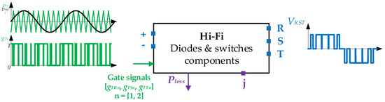
Figure 10.
Hi-Fi model block. (Left) DC voltage nodes and the gate input Pulse Width Modulation (PWM) signal, gTx. (Right) The AC R,S,T terminals and the AC voltage waveform. On the lower side, the thermal and power variables are shown.
The inputs of the model are the switching orders of the active switches (pulsed logical signals), which were obtained from the modulation block; so, depending on the modulation strategy, the input signal will be different.
Taking into account that the Hi-Fi is the most accurate model developed, it needs to provide the highest detail waveforms, representing in detail the waveforms during the switching period. Therefore, its required simulation step must be much smaller than the switching period of the semiconductors.
The Hi-Fi model offers the possibility of using different semiconductor electrical variants depending on the accuracy needed on power losses and output voltage calculation. The electrical variants can be configured before running the simulation, depending on the accuracy and detail levels required by the user. There are up to 150 different combinations to simulate the electrical behavior of the M-Fi model. However, since the Hi-Fi model is based on a dedicated electrical simulator, changing between different variants is not straightforward and the results are complex in comparison with the other developed models.
3.2. M-Fi Model
The objective of the M-Fi model is to offer a model that is mathematically equivalent to the Hi-Fi model, but runs in an equation based simulator instead of in a dedicated physical or electrical simulator. Considering the equations that define the behavior of the semiconductors and taking into account the different switching states of the inverter, it is possible to model the whole inverter in simpler equation based simulators, which does not involve software limitations and is more accessible. This model can be implemented in platforms like MATLAB, C, Excel, etc.
The equation based simulation model results in faster simulations than with the Hi-Fi model as demonstrated by the comparison results shown later in this paper. Moreover, the accuracy loss with respect to the most accurate Hi-Fi model variant was relatively low, as will be shown in Section 5. However, it is necessary to remark that these equation based models do not directly consider the interaction between the variables of the inverter as it does the Hi-Fi model, and therefore it is not possible to develop more complex simulations such as short circuits in this environment.
The M-Fi model has the same input switching order signals like those in the Hi-Fi model. Thus, the M-Fi model has to comply with the same simulation step requirements of the Hi-Fi model. Figure 11 represents the basic inputs and outputs structure of the M-Fi model. As can be seen, based on an equation based simulator, the model and its equations have clearly defined the inputs and outputs, which avoids the instantaneous interaction between different equations and notoriously simplifies its computational cost.
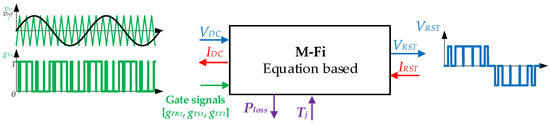
Figure 11.
M-Fi model block. (Left) DC voltage and current, and the gate input PWM signal. (Right) AC voltage and currents. On the lower side, the thermal and power variables are shown.
The M-Fi model offers the possibility of using different electrical variants of the semiconductor depending on the accuracy needs regarding power losses and output voltage calculation. There are 150 different combinations to simulate the electrical behavior of the M-Fi model altogether. In comparison with the Hi-Fi model, these variants can be easily configured before running the simulation, as the model is developed in an equation based simulator that simplifies the configuration procedure.
3.3. Lo-Fi Model
The objective of the Lo-Fi model is to have a faster simulation compared to the M-Fi model. Thus, the reduction in the simulation time will inevitably involve a slight accuracy loss with respect to the Hi-Fi and M-Fi models. Therefore, as with the M-Fi model, the Lo-Fi model cannot simulate circuital-coupled effects such as short circuits, since it is implemented in pure equation based simulators.
As shown in Figure 12, there are two main differences between the Lo-Fi and the M-Fi model. On one hand, the input signal in this case is a low frequency signal (sinusoidal, third harmonic, space vector, classic PWM…) and represents the reference signal of the modulation. On the other hand, the simulation step is, in this case, the same as the switching period of the semiconductors, which means that it is considerably higher than in the M-Fi model. The aim of the Lo-Fi model is to avoid the switched output voltage of the inverter and to simulate the model using a longer simulation step, this way resulting in a much faster simulation model than previously introduced in the Hi-Fi and M-Fi models.
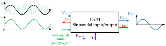
Figure 12.
Lo-Fi model block. (Left) DC voltage and current, and the gate input low frequency PWM signal. (Right) AC voltage and currents. On the lower side, the thermal and power variables are shown.
As can be seen in Figure 12, in this model, the output signal is an equivalent signal of the input low frequency reference signal. Specifically, this output signal corresponds to the first harmonic of the switched output signal that is obtained in real inverters (i.e., the output signal of the Hi-Fi model). The switching behavior of the converter and its resulting output are neglected in this case.
The Lo-Fi model offers the same variants as the M-Fi model. In total, there are 150 different electrical variants, easily exchangeable, depending on the required accuracy for the power losses and the output voltage calculation.
3.4. Fast Lo-Fi Model
The objective of the Fast Lo-Fi model is to increase the simulation speed, even faster than the Lo-Fi model. The Fast Lo-Fi model is also an equation based model, therefore, as in previously explained in the M-Fi and Lo-Fi models, it is not possible to simulate short-circuits. Among the equation based models, the Fast Lo-Fi is the least accurate model due to its higher simulation step, although this also results in the fastest simulation speed.
The Fast Lo-Fi model has the same structure as the Lo-Fi model, but, in this case, the simulation step is greater than the switching period of the semiconductors, so the conduction and switching losses are calculated by taking into account more than one switching period. The model averages the total losses in that given number of periods. Although a higher simulation step results in a faster simulation model, the maximum step size must be limited to guarantee an appropriate sinusoidal output signal. Common sampling criteria consider that at least 20 points per period are necessary to generate an accurate sinusoidal signal. Therefore, the maximum step size is limited to guarantee that criterion, taking into account the highest possible fundamental frequency of the input signal.
The input signal is a low frequency reference signal such as in the Lo-Fi model. Regarding the resulting output signal, it will also be a low frequency signal as in the Lo-Fi model, except that in this case, the sampling will be notorious due to the higher simulation step (Figure 13).
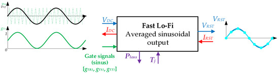
Figure 13.
Lo-Fi model block. (Left) DC voltage and current, and the gate input low frequency PWM signal. (Right) AC voltage and currents. On the lower side, the thermal and power variables are shown.
The number of possible variants is the same as with the previous models, i.e., 150.
3.5. Model Summary
To sum up, Table 1 shows a comparison between the different inverter’s electrical behavior modeling approaches introduced along in this section. It must be highlighted that all variants are implementable in all models.

Table 1.
Summary table of the four different models.
4. Inverter Thermal Variants
In order to allow for accurate temperature dependent modeling of the inverter semiconductors, the dynamic thermal model of junction-to-case, case-to-heatsink, and heatsink-to-ambient behavior is required for each of them. While the semiconductors loss model describes the instantaneous power dissipation of each of them at a given junction temperature, the thermal model determines the temperature gradients across the semiconductor chip, package, and heatsink as a result of power losses being injected by each semiconductor in the thermal network [14,25,26].
For the sake of simplicity and data availability constraints, the case-to-heatsink behavior was neglected in the developed model. Hence, the case and heatsink temperature became the same and only Zth,j-cs (instead of Zth,j-c and Zth,c-s) was considered.
4.1. Junction-to-Case Thermal Model
To represent the thermal behavior of the semiconductor, the physical structure of the device can be represented as a RC structure. Foster and Cauer models are the most commonly used approaches for modeling thermal behavior [27]. The Cauer model represents the real physical behavior of materials inside each thermal layer. Instead, a Foster network does not represent any physical layer, but represents a model that mathematically behaves like a Cauer model, reducing the complexity of the model while maintaining its accuracy. For this reason, Foster networks were used as the reference thermal models (Figure 14).
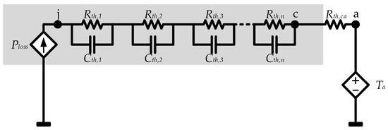
Figure 14.
n layer Foster thermal circuit of a semiconductor. From junction temperature to ambient temperature, where the semiconductor is marked by a grey area.
The aim of the thermal equivalent models was to obtain the junction temperature of each semiconductor (six diodes and six switches in 2L-VSC) from the power losses generated by each of them.
These thermal variants were independent of the previously explained electrical variants and were compatible with all of the electrical modeling approaches.
Three different variants were proposed to calculate the junction-to-case temperature of the semiconductor: an individual n-stage thermal model (12 × n RC), a simplified single stage thermal model (12 × 1 RC) and a global equivalent inverter thermal model (1 × n RC).
4.1.1. Individual n-Stage Thermal Model (12 × n RC)
The individual n-stage thermal model is based on the Foster theoretical model (Figure 15). Despite the fact that this model does not represent each layer of the semiconductor and is not a real representation of the semiconductor, its parameters can be found in datasheets and it is a useful model to calculate the junction temperature of the semiconductors. Although theoretically this model can be extended up to n RC pairs, the datasheets usually provide the parameters of 3 to 5 series RC pairs.
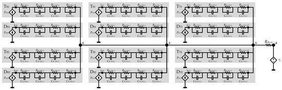
Figure 15.
Equivalent thermal circuit of the two level three-phase inverter, where each semiconductor Foster circuit is marked with a grey area.
Thus, to represent a general scheme of the semiconductors, and based on the Foster model, each diode and switch has n different pair of parallel resistance-capacitor, so the thermal model of a 2L-VSC will consist of 12 × n RCs (Figure 15).
The thermal behavior of each semiconductor can be modeled using a transfer function for each pair of parallel resistance-capacitor as can be seen in Figure 16, where its input is the semiconductor’s power loss and the output will be the junction (j)-to-case (c) temperature.
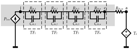
Figure 16.
n layer semiconductor’s Foster circuit, where each pair of RCs can be transformed into a transfer function.
The parameters that define the thermal transfer functions of the state-of-the-art semiconductors’ are usually provided in their datasheets, by means of several resistance (Rth,i) and time constant (τi) pairs, each of them referring to a cascaded Foster RC pair.
Therefore, the junction-to-case model of each semiconductor is defined by the sum of n different transfer functions (Equations (27)–(29)) [28].
The required block diagram in the equation-based simulator will look like that in Figure 17 for each semiconductor:
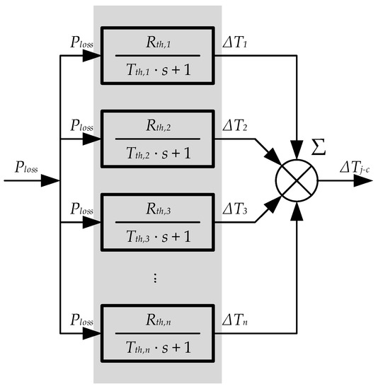
Figure 17.
Semiconductor temperature calculation via transfer functions. The software under use is Simulink.
4.1.2. Simplified Single Stage Thermal Model (12 × 1 RC)
In order to reduce complexity and simulation time, the individual n-stage thermal model can be simplified to a single RC pair for each semiconductor, resulting in 12 × 1 RCs for the whole inverter. By means of the least squares technique, the equivalent individual RC pair that minimizes the accuracy error can be deduced for each semiconductor, notoriously simplifying the thermal circuit model (Figure 18). This way, the simulation time will be shorter without compromising accuracy, as will be shown later in Section 5.
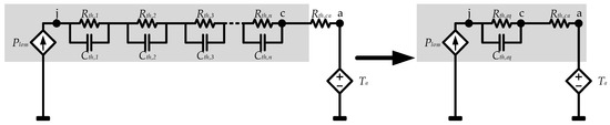
Figure 18.
Simplification of the semiconductor thermal Foster model from 12 × n RCs to 12 × 1 RCs.
Thus, considering the 12 semiconductors of a 2L-VSC, a 12 × 1 simplified RC network model can be obtained for the complete inverter (Figure 19).
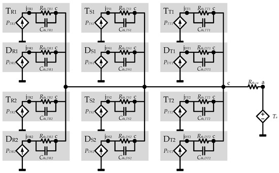
Figure 19.
12 × 1 simplified RC network model. Each semiconductor is marked by a grey area.
4.1.3. Global Equivalent Inverter Thermal Model (1 × n RC)
With the aim of further reducing the simulation time, instead of calculating the junction temperature of each semiconductor, the same average temperature could be assumed for all of the devices, that is to say, a unique equivalent inverter junction temperature. For that, an equivalent global thermal circuit and its according transfer function need to be calculated.
For that purpose, it was supposed that all the diodes and switches had the same n number of RC pairs, as was previously shown in Figure 15.
Figure 20 depicts how this approaching process is carried out. Assuming that each semiconductor’s thermal network is modeled with the same n number of RC pairs, the parallel connection of the thermal resistances and capacitances contained in the same layer (i = 1, 2, 3, …n) of all the different semiconductors is considered. Thus, the accurate thermal circuit shown in 12 × n model can be converted into a less complex 1 × n RC pairs thermal circuit (Figure 20).
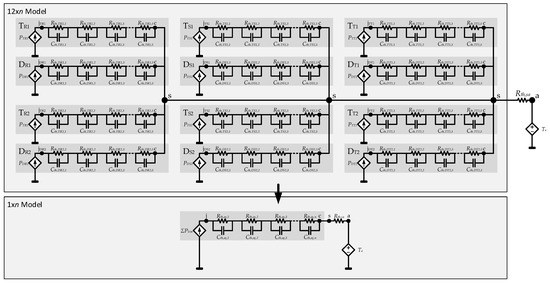
Figure 20.
12 × n RC to 1 × n RC simplification. Each semiconductor’s thermal model is shaded in dark grey.
The thermal parameters of each RC Foster pair are obtained by means of Equations (30) and (31).
Then, n different transfer functions are defined by means of Equation (32).
Consequently, the block diagram shown in Figure 21 will represent the 1 × n RC thermal circuit in the equation based simulator, which corresponds to the total equivalent transfer function of Equation (33).
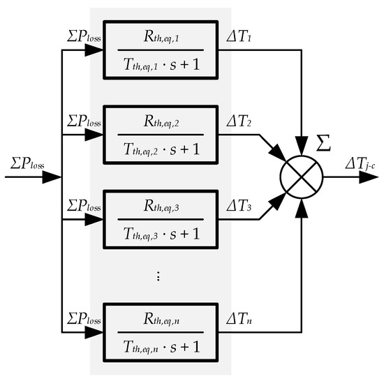
Figure 21.
Equation based simulator block diagram to obtain the 1 × 1 RC model.
This approach provides a much faster simulation although it involves a considerable accuracy loss in comparison with the individual n-stage thermal model, especially regarding the temperature ripple and the unbalanced temperature distribution. However, it can be a very interesting tool from the point of view of any EV manufacturer, as it allows simulating long periods of EV operation in a short period of time.
4.2. Heatsink-to-Coolant Output Behavior (ΔTsa Calculation)
The thermal behavior from heatsink-to-coolant is highly dependent on the mechanical setup of the heat exchanger and on the cooling parameters like flow rate and coolant inlet temperature. Therefore, unlike junction-to-heatsink behavior, the transfer function coefficients (Rth,sa,n, τth,sa,n) are not constant.
As a baseline for the heatsink model, a public available datasheet of a SEMIKRON SKiiP 1814 GB17E4-3DUW power module was used, which defines the transfer function of heatsink by a second order Foster network (Equation (34)).
where Rth,sa,1, Rth,sa,2 and τth,sa,1, τth,sa,2 are the parameters of a second order foster network.
For accurate modeling of thermal behavior, the effect of coolant temperature and flow rate on thermal impedance must be taken into account using data available from datasheets. The variation of the transfer function coefficients (Rth,sa,1, Rth,sa,2, and τth,sa,1, τth,sa,2) with respect to flow rate and inlet coolant temperature was introduced by means of lookup tables, which were derived from the formula given in a SEMIKRON application note [29] via the MATLAB script. A fixed water to glycol ratio for coolant was assumed.
5. Analysis of the Inverter Model Accuracy
This section collects the results of the different electrical and thermal models’ accuracy analyses. The implemented models of the inverter were validated via simulation. The idea of these analyses was to compare the results obtained by the Hi-Fi model (reference), and the other M-Fi, Lo-Fi, and Fast Lo-Fi models. The results described here were obtained for the operating point in Table 2.
Table 2.
A comparison of the operating point data for the electrical models.
In order to analyze the accuracy of the different models, both electrical and thermal variables were taken into account.
Table 3 shows a summary of the comparison results for the different models. Regarding the power losses estimation, a 6.49% accuracy error was made in the total power losses estimation with the less accurate Fast Lo-Fi model. However, the error made in the individual semiconductors’ losses and average junction temperature estimation seems to be below 3% in all cases.
Table 3.
Accuracy comparison between the different inverter physical models.
Regarding other electrical variables such as output voltage and current fundamental harmonics, accuracy losses below 6% were obtained with different modeling approaches. Only the DC-link average current estimation seemed to result in worse accuracy performance, especially with the Fast Lo-Fi model. Section 5.1 and Section 5.2 analyze the electrical and thermal behavior results in detail.
5.1. Comparison of Electrical Models
The conduction losses, the switching losses, and the output voltage of the inverter were compared in the first term. The Hi-Fi and M-Fi models offered a very close performance, as demonstrated by the results in Table 3. The waveforms obtained with Hi-Fi and M-Fi models were also very similar; hence, for the detailed comparison between the rest of the modeling approaches, only the Hi-Fi model waveforms are considered. All of the comparison tests were carried out for the working point described in Table 2.
5.1.1. Conduction Losses Comparison
In Figure 22, the conduction losses obtained with Hi-Fi, Lo-Fi, and Fast Lo-Fi models are shown. The compared waveforms show that the three models provide different results. The delay effect of the larger sample time of the Fast Lo-Fi model can be easily seen in Figure 22. The same delay effect can also be seen with the Lo-Fi model, where the smaller step size provides a closer estimation regarding the reference Hi-Fi model waveform.
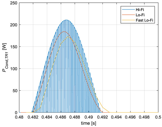
Figure 22.
Hi-Fi, Lo-Fi, and Fast Lo-Fi conduction losses comparison.
Despite the obvious delay between different modeling approaches, the average conduction losses estimated for the Lo-Fi and Fast Lo-Fi models during a fundamental output period were very close to the ones obtained with the Hi-Fi model, as summarized in Table 4. It can be concluded that the error was lower than 7% in the worst case.
Table 4.
Average conduction power losses in Hi-Fi, Lo-Fi, and Fast Lo-Fi models.
5.1.2. Switching Losses Comparison
Regarding the switching losses, a similar conclusion can be obtained from the example provided in Figure 23. The Lo-Fi model generates an averaged waveform of the Hi-Fi model waveform. Although it rejects the instantaneous switching losses peaks that appear in the most accurate Hi-Fi model, the Lo-Fi model accurately follows the average value of these losses. Again, the higher the simulation step, the greater the delay that appears between the accurate Hi-Fi model and the Lo-Fi and Fast Lo-Fi models.
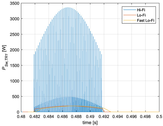
Figure 23.
A comparison of the Hi-Fi, Lo-Fi, and Fast Lo-Fi switching losses.
However, considering the average switching losses along a fundamental period, the resulting accuracy error was considerably low with both the Lo-Fi and Fast Lo-Fi approaches, as summarized in Table 5. It can be concluded that in the worst case, the error was lower than 1%.
Table 5.
Average switching power losses in the Hi-Fi, Lo-Fi, and Fast Lo-Fi models.
5.1.3. Output Voltage Comparison
Regarding the inverter’s output voltage comparison, Figure 24 shows the waveforms obtained for the different modeling approaches.
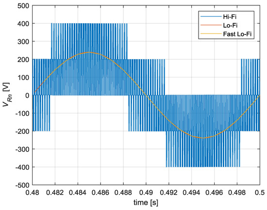
Figure 24.
Comparison of the Hi-Fi, Lo-Fi, and Fast Lo-Fi output voltage.
The main difference between the three models can be seen at a glance in Figure 24. While the output waveform of the Hi-Fi model was a pulsed signal, the Lo-Fi and Fast Lo-Fi models’ waveforms were equivalent to the controller’s reference low frequency signals. Furthermore, as seen in the conduction and switching power losses, the higher simulation step size resulted in a higher delay in the waveforms.
5.2. Thermal Model Comparison
In this section, the simulation results obtained with the three different variants of the inverter thermal model are compared.
In this case, the three thermal variants were compared considering only the electrical M-Fi model, with a simulation step of 1e-5 s. These results were also been obtained for the working point described in Table 2.
5.2.1. Individual n-Stage Thermal Model (12 × n RC) vs. Simplified Single Stage Thermal Model (12 × 1 RC)
First, the individual n-stage (12 × n RC) and the simplified single stage (12 × 1 RC) thermal models were compared. The evolution of the junction temperature of a given switch and a diode can be seen in Figure 25 for both models.
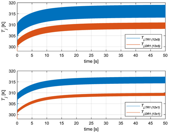
Figure 25.
Comparative between individual n = 5-Stage (12 × 5 RC) (above) and simplified single stage (12 × 1) (below) thermal models.
The upper plot in Figure 25 shows the transient state of the junction temperature of the TR1 active switch and the DR1 diode with the most accurate 12 × 5 RC thermal model (n = 5 RC pairs were considered). The waveforms showed that both semiconductors had similar junction temperatures and evolution in time, but they were not equal, since they dissipated different power losses and their associated thermal circuit parameters were different.
A similar conclusion can be obtained from the lower plot in Figure 25 where the same variables are depicted for the 12 × 1 RC thermal model.
If the waveforms of the active switch junction temperature (Tj,TR1) of both modeling approaches are compared, it can be concluded that both waveforms are similar. From the zoom shown in Figure 26, it can be deduced that the 12 × 1 thermal model approach filters the high frequency (fsw = 5 kHz) ripple that appears in the 12 × 5 thermal model. Moreover, the fundamental frequency ripple (fo = 50 Hz) was also attenuated, and a slight delay phenomenon was observed, as seen with the different electrical approaches in this paper. However, the accuracy error of the average value was less than 1% along all transient states and in the steady state. Hence, it can be concluded that a low accuracy loss is guaranteed when simplifying from a 12 × n RC model to a 12 × 1 RC model.
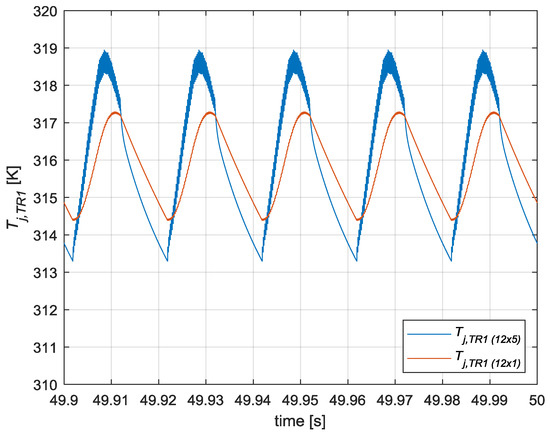
Figure 26.
Zoom of the evolution of TR1 semiconductor junction temperature with the individual 5-stage 12 × 5 thermal model and simplified single stage 12 × 1 thermal model.
5.2.2. Individual n-Stage Thermal Model (12 × n RC) vs. Global Equivalent Inverter Thermal Model (1 × n RC)
After observing the good accuracy provided by the 12 × 1 RC thermal model, the accuracy of the most simplified global equivalent model 1 × n RC model was also analyzed. The results can be seen in Figure 27 for a n = 5 configuration.
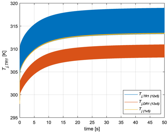
Figure 27.
Comparison between the junction temperatures of semiconductors TR1 and DR1 obtained with the Individual 5-stage 12 × 5 thermal model and the equivalent Tj temperature obtained with the global equivalent 1 × 5 RC thermal model.
Figure 28 shows a zoom of the temperature evolution from Figure 27. As can be clearly seen, the resulting waveform was different from any temperature waveform obtained with previous modeling approaches. The resulting temperature waveform rejected the junction temperature ripples generated at the switching (fsw = 5 kHz) and fundamental (fo = 50 Hz) frequencies. However, an accurate averaging effect among the different semiconductors temperatures can be clearly seen.
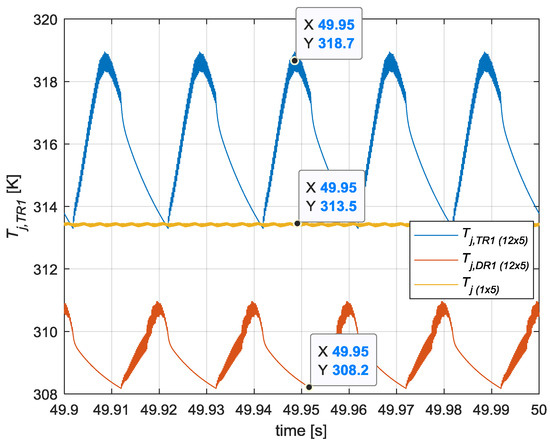
Figure 28.
Zoom of the evolution of TR1 and DR1 semiconductors junction temperature obtained with individual 5-stage 12 × 5 thermal model and equivalent Tj temperature obtained with the global equivalent 1 × 5 RC thermal model.
5.3. Accuracy Analysis in Different Operating Conditions
The accuracy analysis was extended to several working conditions of the inverter, which could represent different scenarios mainly regarding high/low speed conditions and motoring/braking operation. All the analyzed scenarios showed the same trend in terms of accuracy when considering the four different modeling approaches. For instance, Table 6 presents the results corresponding to a medium-speed and hard braking scenario.
Table 6.
Accuracy comparison between different inverter physical models for a braking scenario (Vll,rms,1 = 294 V, Iph,rms,1 = 600 A, cos ϕ = −0.97 (regenerating), fo = 50 Hz.
6. Analysis of the Inverter Model Simulation Speed
This section describes the simulation speed comparison between the different developed models. Two different comparisons were carried out. On one hand, the electrical models’ simulation speed was analyzed, considering the same thermal model (12 × 5 RC) in all simulations. On the other hand, the thermal models’ simulation speed was analyzed by considering the different electric modeling approaches.
6.1. Speed Analysis of the Electrical Models
The objective of this comparison was to demonstrate that the less detailed the model, the faster the simulation. In this case, two different variant combination of the models were considered: the most detailed one (Full detail) considering the most complex electro-thermal coupling combinations and the simplest one (Null detail), in which the ideal voltage drop, conduction losses, and switching losses are considered.
In order to represent the resulting simulation speed with different modeling combinations and scenarios, the ratio between the time taken to complete the simulation (Real time) and the Simulated time were compared. If this ratio is higher than 1, it means that the simulation is slower than the real time. On the contrary, if the ratio is lower than 1, the simulation is faster than in real time. Table 7 summarizes the obtained results.
Table 7.
Speed comparison of the electrical models where the relation between the real time and the simulated time is shown.
The results demonstrate that the Hi-Fi models were significantly slower than any of the other modeling approaches. This is why Hi-Fi models are only useful for very specific use where the maximum accuracy needs to be obtained, regardless of the simulation speed (specific failure tests, short circuits, etc.).
The M-Fi model provided a remarkable improvement in terms of simulation speed in comparison with the Hi-Fi model. Although it could not guarantee a real time simulation capability, it provided a simulation about 100 times faster than its equivalent Hi-Fi model with a minimum accuracy loss. Moreover, the results showed that there was a significant reduction in the simulation time between full and null detail models. The null detail model avoids many calculations that resulted in a notorious computational cost improvement. The simulation time was improved by 34% from the full to null detailed models.
Regarding the Lo-Fi and Fast Lo-Fi models, the time improvement between the full and null detail models was about 38% in both cases. It should be highlighted that with both the Lo-Fi and Fast Lo-Fi models, the simulation time was reduced over 20 times in comparison to their equivalent M-Fi models. This reduction in simulation time allows for these models to be run in real time.
6.2. Speed Analysis of the Thermal Models
The objective of this comparison was to demonstrate the improvement in simulation time provided by the different thermal model approaches.
As can be seen in Table 8, the different 12 × 1 RC and 1 × 5 RC thermal approaches provided a remarkable reduction in the simulation time, especially with the Lo-Fi and Fast Lo-Fi models, where the time can be reduced to half.
Table 8.
A speed comparison of the thermal models, where the relation between the real time and simulated time is shown.
7. Conclusions
The rapidly increasing EV market demands the continuous optimization of simulation and designing tools. The inverter of an EV, which usually operates in the range of a few to tenths of kHz, can demand the specific and detailed simulation of a few microseconds or milliseconds for short time electric response analysis as well as long-term simulations for slow thermal response analyses. This paper introduced a simple and versatile simulation tool for an EV inverter, which can easily adapt to these different simulation objectives.
For that purpose, four different modeling accuracy levels were developed (Hi-Fi, M-Fi, Lo-Fi, and Fast Lo-Fi), which provide faster simulation speed as the accuracy requirements are eased. Each of the four modeling approaches divides the electric behavior of the semiconductors and thereby the inverter into the voltage drop, conduction losses, and switching losses estimation. Each of the electric phenomenon can also be approached by different modeling variants, providing up to 150 combinations for the electrical modeling of the inverter.
Furthermore, the thermal behavior of the semiconductors and thus the whole inverter were also modeled by three different variants, providing different accuracy/simulation speed performances. The combination of the available electrical and thermal variants provided up to 450 modeling options for each of the four accuracy levels (Hi-Fi, M-Fi, Lo-Fi, and Fast Lo-Fi) considered.
The accuracy and simulation speed of the different models were compared in the simulation. The results showed that an accuracy error below 7% was guaranteed with different modeling approaches in most of the analyzed scenarios when estimating the semiconductors’ average power losses and junction temperatures as well as the inverters’ fundamental output current and voltages.
In comparison with the most detailed accuracy level (Hi-Fi model), where a specific electrical simulator is required, the equation based models (M-Fi, Lo-Fi and Fast Lo-Fi) maintained acceptable accuracy levels in terms of instantaneous waveforms and average values while reducing the simulation time by more than 100 times. The Lo-Fi and Fast Lo-Fi models could also allow for the running of real time simulations.
Regarding the thermal models, the most detailed 12 × n individual model can be easily exchanged for the less complex 12 × 1 model, which accurately approaches the different semiconductors’ junction temperatures with less computational cost and faster simulations. The 1 × n model averages the different semiconductors’ thermal behavior and estimates a single junction temperature for the whole inverter. Although this model is not useful in determining the temperature ripple in the semiconductors and identifying the thermal stress distribution among semiconductors, it can be a valuable tool for long term simulations, since it can reduce the simulation time to half in comparison to the most detailed 12 × n model.
Author Contributions
Conceptualization, J.U., M.M., A.A., I.A., M.V. and R.K.; Investigation, J.U., M.M., A.A. and I.A.; Writing—original draft, J.U., M.M., A.A. and I.A.; Writing—review & editing, S.C., O.H., M.V. and R.K.
Funding
This project has received funding from the European Union’s Horizon 2020 research and innovation programme under grant agreement No 769935. 
Conflicts of Interest
The authors declare no conflict of interest.
References
- Newwire, P.R. Electric Vehicle Market—Global Forecast to 2025: Market is Dominated by Tesla, Nissan, BYD, BMW and Volkswagen; Global Market Insights, Inc.: Selbyville, DE, USA, 2018. [Google Scholar]
- McKerracher, C. EV Market Trends and Outlook; New Energy Financ.: London, UK, 2017. [Google Scholar]
- DiChristopher, T. Electric Vehicles will Grow from 3 million to 125 million by 2030: IEA Forecasts. 2018. Available online: https://www. cnbc. com/2018/05/30/electric-vehicles-will-grow-from-3-million-to-125-millionby-2030-iea. html (accessed on 26 September 2018).
- Zhou, Z.; Kanniche, M.S.; Butcup, S.G.; Igic, P. High-speed electro-thermal simulation model of inverter power modules for hybrid vehicles. IET Electr. Power Appl. 2011, 5, 636. [Google Scholar] [CrossRef]
- Bryant, A.; Roberts, G.; Walker, A.; Mawby, P.; Ueta, T.; Nisijima, T.; Hamada, K. Fast Inverter Loss and Temperature Simulation and Silicon Carbide Device Evaluation for Hybrid Electric Vehicle Drives. IEEJ Trans. Ind. Appl. 2008, 128, 441–449. [Google Scholar] [CrossRef][Green Version]
- Hifi-Elements|High Fidelity Electric Modelling and Testing. Available online: https://www.hifi-elements.eu/hifi/ (accessed on 20 September 2019).
- Inokuchi, S.; Saito, S.; Izuka, A.; Hata, Y.; Hatae, S.; Nakano, T.; Motto, E.R. A new high capacity compact power modules for high power EV/HEV inverters. In Proceedings of the 2016 IEEE Applied Power Electronics Conference and Exposition (APEC), Long Beach, CA, USA, 20–24 March 2016; pp. 468–471. [Google Scholar]
- Hussein, K.; Ishihara, M.; Miyamoto, N.; Nakata, Y.; Nakano, T.; Donlon, J.; Motto, E. New compact, high performance 7th Generation IGBT module with direct liquid cooling for EV/HEV inverters. In Proceedings of the 2015 IEEE Applied Power Electronics Conference and Exposition (APEC), Charlotte, NC, USA, 15–19 March 2015; Volume 2015, pp. 1343–1346. [Google Scholar]
- Murakami, Y.; Tajima, Y.; Tanimoto, S. Air-cooled full-SiC high power density inverter unit. In Proceedings of the 2013 World Electric Vehicle Symposium and Exhibition (EVS27), Barcelona, Spain, 17–20 November 2013; pp. 1–4. [Google Scholar]
- Chakraborty, S.; Lan, Y.; Aizpuru, I.; Mazuela, M.; Alacano, A.; Hegazy, O. Scalable and Accurate Modelling of a WBG-based Bidirectional DC/DC Converter for Electric Drivetrains. In Proceedings of the 32nd Electric Vehicle Symposium (EVS32), Lyon, France, 19–22 May 2019; pp. 1–11. [Google Scholar]
- Rao, N.; Dinesh, C. Calculating Power Losses in an IGBT Module; Appllication Note AN6156-1; Dynex Semiconductor Ltd.: Lincoln, Lincolnshire, UK, 2014. [Google Scholar]
- Blinov, A.; Vinnikov, D.; Jalakas, T. Loss calculation methods of half-bridge square-wave inverters. Elektron. Elektrotechnika 2011, 7, 9–14. [Google Scholar] [CrossRef]
- Zhou, Z.; Khanniche, M.S.; Igic, P.; Kong, S.T.; Towers, M.; Mawby, P.A. A fast power loss calculation method for long real time thermal simulation of IGBT modules for a three-phase inverter system. Int. J. Numer. Model. Electron. Netw. Devices Fields 2006, 19, 33–46. [Google Scholar] [CrossRef]
- Ma, K.; Bahman, A.S.; Beczkowski, S.; Blaabjerg, F. Complete loss and thermal model of power semiconductors including device rating information. IEEE Trans. Power Electron. 2015, 30, 2556–2569. [Google Scholar] [CrossRef]
- Graovac, D.; Pürschel, M.; Kiep, A. MOSFET Power Losses Calculation Using the Datasheet Parameters. Infineon Appl. Note 2006, 1, 1–23. [Google Scholar]
- Yao, Y.; Lu, D.C.; Verstraete, D. Power loss modelling of MOSFET inverter for low-power permanent magnet synchronous motor drive. In Proceedings of the 2013 1st International Future Energy Electronics Conference (IFEEC), Tainan, Taiwan, 3–6 November 2013; pp. 849–854. [Google Scholar]
- Williams, B. Power Electronics: Devices, Drivers, Applications, and Passive Components, 2nd ed.; McGraw-Hill Education: New York, NY, USA, 1992. [Google Scholar]
- Munk-Nielsen, S.; Tutelea, L.N.; Jaeger, U. Simulation with ideal switch models combined with measured loss data provides a good estimate of power loss. In Proceedings of the Conference Record of the 2000 IEEE Industry Applications Conference. Thirty-Fifth IAS Annual Meeting and World Conference on Industrial Applications of Electrical Energy (Cat. No.00CH37129), Rome, Italy, 8–12 October 2000; Volume 5, pp. 139–143. [Google Scholar]
- Chakraborty, S.; Sudhanshu, G.; Aizpuru, I.; Mazuela, M.; Klink, R.; Hegazy, O. High-Fidelity Liquid-cooling Thermal Modeling of a WBG-based Bidirectional DC-DC Converter for Electric Drivetrains. In Proceedings of the 21st European Conference on Power Electronics and Applications (EPE ’19 ECCE Europe), Genova, Italy, 2–6 September 2019; pp. 1–8. [Google Scholar]
- Witold, M.; Bartosz, R.; Zbigniew, S. Switching losses in three-phase voltage source inverters. Czas. Tech. 2015, 2015, 47–60. [Google Scholar]
- Pou, J.; Osorno, D.; Zaragoza, J.; Ceballos, S.; Jaen, C. Power losses calculation methodology to evaluate inverter efficiency in electrical vehicles. In Proceedings of the 2011 7th International Conference-Workshop Compatibility and Power Electronics (CPE), Tallinn, Estonia, 1–3 June 2011; pp. 404–409. [Google Scholar]
- Minambres-Marcos, V.; Guerrero-Martinez, M.A.; Romero-Cadaval, E.; Milanes-Montero, M.I. Generic Losses Model for Traditional Inverters and Neutral Point Clamped Inverters. Elektron. Elektrotechnika 2014, 20, 84–88. [Google Scholar] [CrossRef]
- Drofenik, U.; Kolar, J.W. A General Scheme for Calculating Switching- and Conduction-Losses of Power Semiconductors in Numerical Circuit SImulations of Power Electronic Systems. In Proceedings of the 2005 International Power Electronics Conference, IPEC-Niigata 2005, Niigata, Japan, 4–8 April 2005. [Google Scholar]
- Wu, B.; Narimani, M. High-Power Converters and AC Drives, 2nd ed.; John Wiley & Sons, Inc.: Hoboken, NJ, USA, 2016. [Google Scholar]
- März, M.; Nance, P. Thermal Modeling of Power Electronic Systems; Infineon Technol. AG Munich: Neubiberg, Germany, 2000; pp. 1–20. [Google Scholar]
- Fakhfakh, M.A.; Ayadi, M.; Neji, R. Thermal behavior of a three phase inverter for EV (Electric Vehicle). In Proceedings of the Melecon 2010—2010 15th IEEE Mediterranean Electrotechnical Conference, Valletta, Malta, 26–28 April 2010; pp. 1494–1498. [Google Scholar]
- Infineon Technologies. Transient Thermal Measurements and Thermal Equivalent Circuit Models; Application Note AN 2015-10; Infineon Technologies AG.: Neubiberg, Germany, 2018; pp. 1–13. [Google Scholar]
- Irwin, J.D.; Nelms, R.M. Basic Engineering Circuit Analysis, 10th ed.; John Wiley & Sons, Inc.: Hoboken, NJ, USA, 2011. [Google Scholar]
- SEMIKRON. Estimation of Liquid Cooled Heat Sink Performance at Different Operation Conditions; Appllication Note AN1501; Semikron: Nuremberg, Germany, 2015; pp. 1–12. [Google Scholar]
© 2019 by the authors. Licensee MDPI, Basel, Switzerland. This article is an open access article distributed under the terms and conditions of the Creative Commons Attribution (CC BY) license (http://creativecommons.org/licenses/by/4.0/).