Article

A Modified One-Cycle Control for Vienna Rectifiers with Functionality of Input Power Factor Regulation and Input Current Distortion Mitigation †

School of Mechanical electronic & Information Engineering, China University of Mining & Technology, Beijing 100083, China
*
Author to whom correspondence should be addressed.
This paper is an extended version of our paper published in the 2018 3rd International Conference on Insulating Materials, Material Application and Electrical Engineering (IMMAEE 2018), Melbourne, Australia, 15–16 September 2018.
Energies 2019, 12(17), 3375; https://doi.org/10.3390/en12173375
Submission received: 14 July 2019 / Revised: 28 August 2019 / Accepted: 29 August 2019 / Published: 2 September 2019

Abstract

:
In this paper, aiming at incorporating reactive power compensation functionality into the Vienna rectifiers, a modified one-cycle-control (MOCC) strategy is proposed by which the three-phase Vienna rectifier can be regulated in leading, lagging or unity power factors with near-sinusoidal input current waveform. First, a brief review of the working principle of the conventional OCC (COCC) strategy is conducted. Then, the MOCC strategy with the functionality of input current phase-shift control is discussed in detail. To mitigate input current distortion caused by the current phase-shift, a method whereby the signal of one phase current which is flowing in an uncontrollable region is injected into the other two phases’ current command signals is further presented. The constraints to the implementation of the MOCC scheme and the reactive power compensation capacity of the rectifier under MOCC control are analyzed as well. The proposed MOCC strategy is as easy to implement as the COCC strategy. Moreover, the MOCC strategy also preserves all other advantages of the COCC strategy, such as no phase-locked loop, no frame transformation and constant switching frequency. Finally, the theoretical analysis of the proposed MOCC strategy is fully verified by simulation and experimental results from a 1 kV·A three-phase Vienna rectifier prototype.

1. Introduction

Nowadays, power quality (PQ) is seriously influenced by increasing penetration of various power electronic devices connected to the grid. Power electronic devices generally exhibit a nonlinear load characteristic to the power grid, which usually consumes a large amount of reactive power and injects a great deal of harmonics to the line current. In order to reduce the impact of these PQ problems, specifically designed static VAR compensator (SVC), static synchronous compensator (STATCOM) and active power filters (APFs) have been widely used with satisfactory performance for reactive power compensation (RPC) and harmonic current compensation (HCC). However, in recent years, with the increasing application of distributed generation (DG) systems, many researchers believe that compared to those specifically designed pieces of equipment for power quality improvement, incorporating RPC and HCC functionality into existing popularly used bidirectional power converters as the interface of DG systems may be a more cost-effective solution for power quality management [1,2,3]. A significant advantage of this solution in power quality management is that the local compensation of reactive power will eliminate the extra power loss due to long-distance transmission of reactive power and does not require additional hardware costs.
However, in quite a lot of practical applications, such as the front end of power converters for alternating current (AC)speed regulation with pumps or fan loads, switching the power supply for telecommunications and electric vehicles (EV) battery chargers for level I, etc., unidirectional power converters are usually the preferable choices. Compared to bidirectional converters, unidirectional power converters use fewer fully controlled power switches, simpler controllers, and have lower power losses as well as lower cost for implementation. Taking this consideration into account, many researchers have also been investigating the possibility of incorporating RPC and HCC functionalities into unidirectional power converters [4,5].
In [6] and [7], Vienna rectifiers with added active filter functionality in three-phase three-wire and three-phase four-wire systems have been reported, respectively, but integrating reactive power compensation function into Vienna rectifiers is not mentioned in either study. In [8], integrating harmonic current compensation (HCC) and reactive power compensation (RPC) functionality into the Vienna rectifiers is investigated, and a conclusion is given based on theoretical analysis, which states that because of the unidirectional power flow characteristic, Vienna rectifiers have only limited RPC capability. In [8], how to enhance the RPC capability for unidirectional converters is not further studied, so although [8] studied incorporating RPC functionality into traditional unidirectional power converters, the discussion is far from sufficient.
Incorporating RPC function into conventional unidirectional power converters means the phase angle of the input current of the converter with regard to the source voltage should be able to be shifted in leading or lagging freely. However, because of the unidirectional power flow characteristic of the converter, the input current distortion appears whenever the polarity of the AC side current and voltage of the rectifier become opposite [4,9]. This means that, the larger the phase angle, the higher the input current distortion would be. The input current distortion greatly limits the incorporation of RPC functionality into conventional unidirectional power converters. Up to now, no ideal solutions are discussed to mitigate or even eliminate this input current distortion.
In 1991, K. M. Smedley proposed the one cycle control method, since then, it has become one of the widely used control strategies for single phase and three-phase AC/DC (direct current) pulse width modulation (PWM) converters [10,11,12,13,14,15]. The OCC strategy is often referred to as resistance emulation control. It will force the input current to be in phase with the grid voltage in sinusoidal waveform automatically with no requirement for phase locked loop (PLL), grid voltage sensors and frame transformation, when it is adopted by the boost type PWM rectifiers [16]. These unique features make the OCC much easier to implement. However, despite the aforementioned advantages, COCC does not provide a practical method to make the phase angle of the input current of boost type PWM converters become adjustable. Therefore, the COCC control strategy cannot be used directly to regulate the input power factor of the PWM converters. In addition, in the COCC strategy, the input current of the converter always lags the grid voltage by a small angle due to neglecting the voltage drop of the input inductor, which results in a converter with non-unity power factor displacement [17,18].
Part of this paper has been published at a conference [19]. However, in the conference paper, the capabilities of compensation and the effects of frequency changes for the proposed control strategy were not discussed. Moreover, the experimental validation was not provided as well.
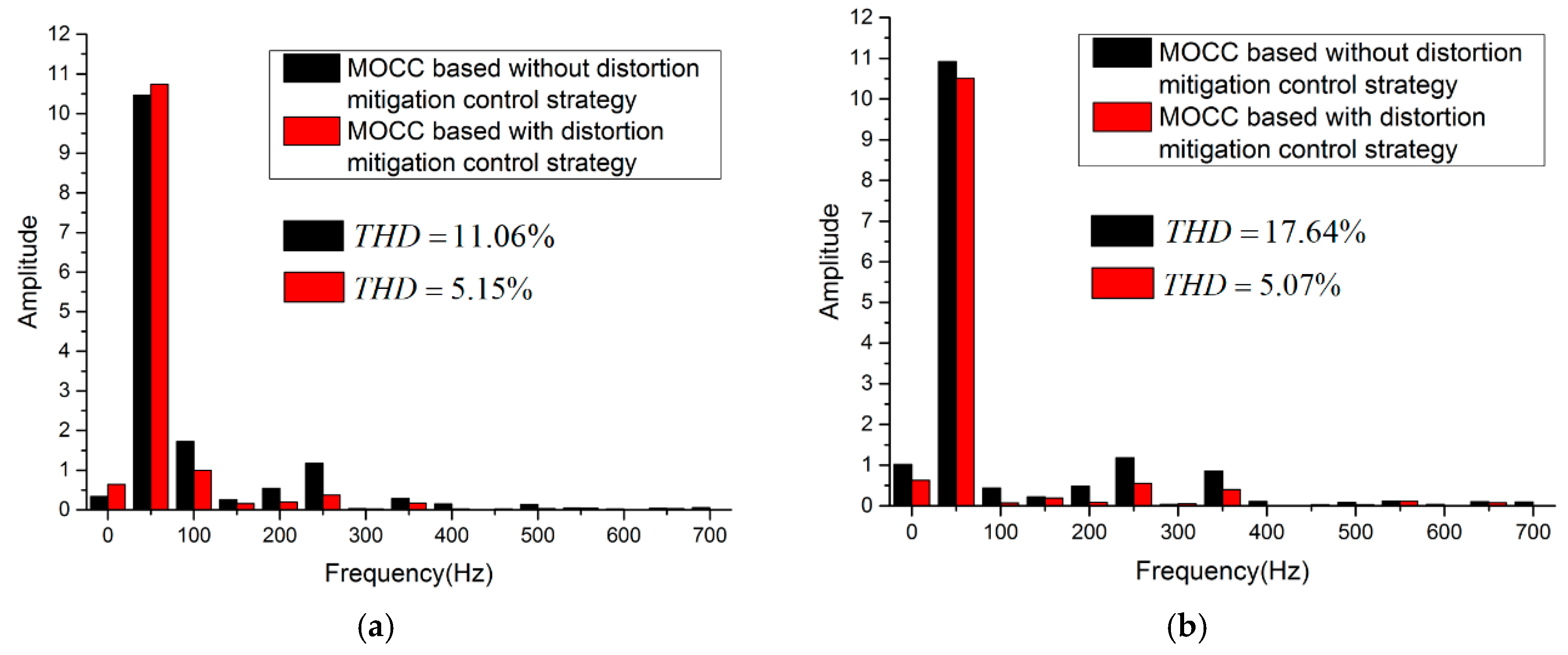
In this paper, a modified one-cycle-control strategy is proposed to achieve phase shift control of the rectifier input current, which makes the Vienna rectifier be able to operate under leading, lagging or unity power factors. A compensation method for mitigating input current distortion caused by phase-shift of the input current is also provided.
The rest of the paper is organized as follows. In Section 2, the operating principle of the COCC strategy is reviewed briefly. On this basis, the MOCC strategy with input current phase-shift control is proposed in Section 3. In Section 4, the cause of the input current distortion with unidirectional power rectifiers is analyzed. To solve this problem, a control strategy to mitigate input current distortion of unidirectional three-phase Vienna rectifiers based on MOCC scheme is proposed in Section 4. Simulations and experimental results are provided in Section 5 to verify the validity of the theoretical findings. Finally, the conclusions are summarized in Section 6.

2. Basic Principles of Conventional OCC

Although the basic operation principle of the three-phase Vienna converter with COCC strategy has been discussed in several papers before, for the sake of completeness, this paper will still start with a brief introduced of it.
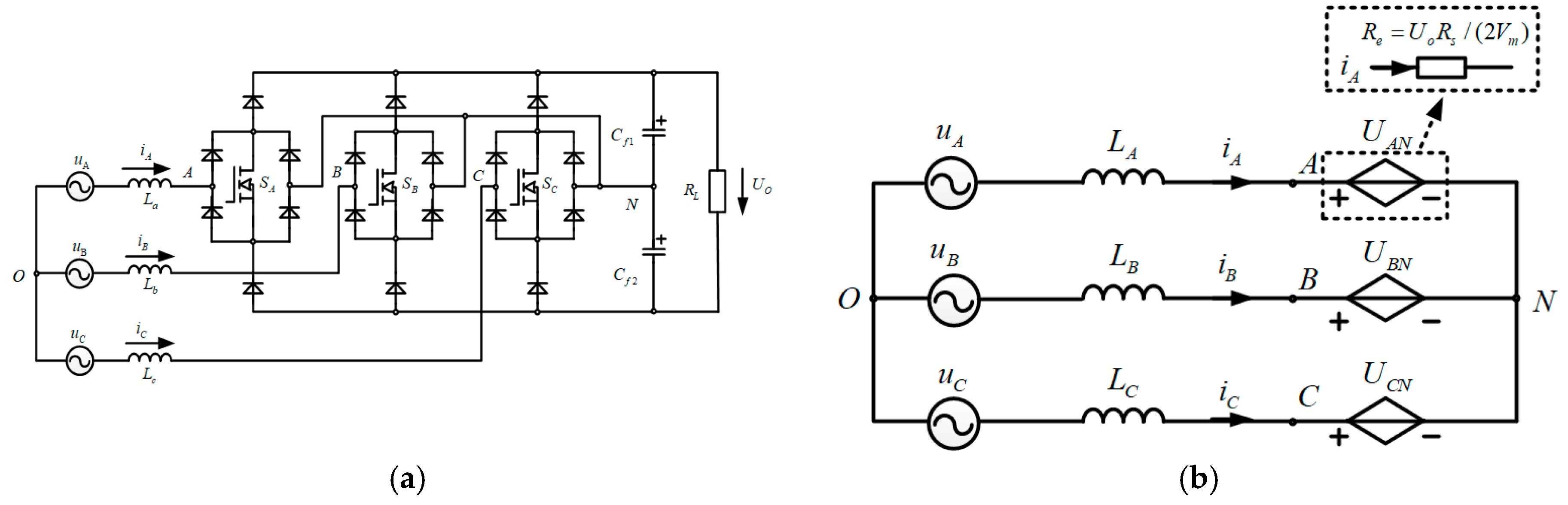
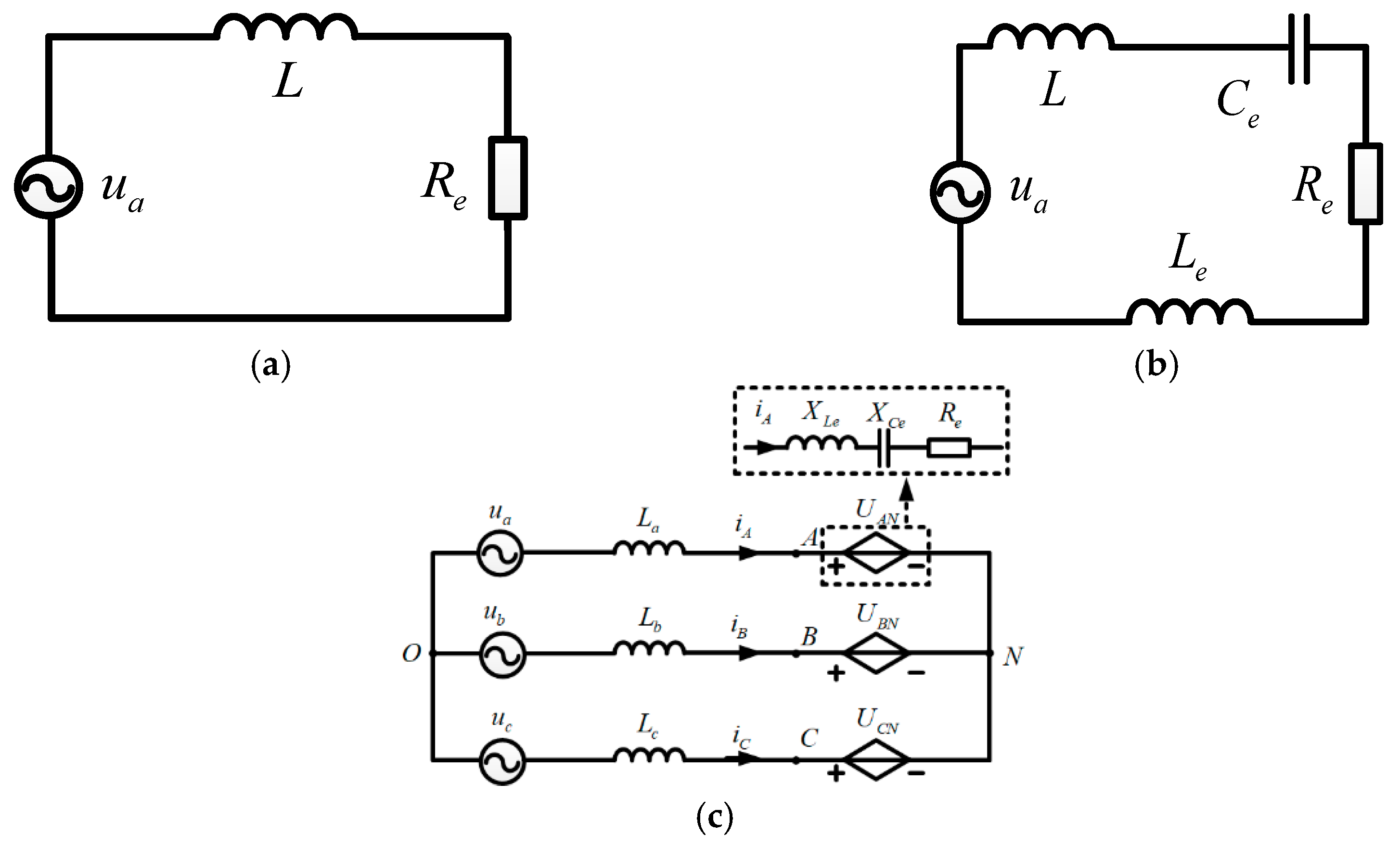
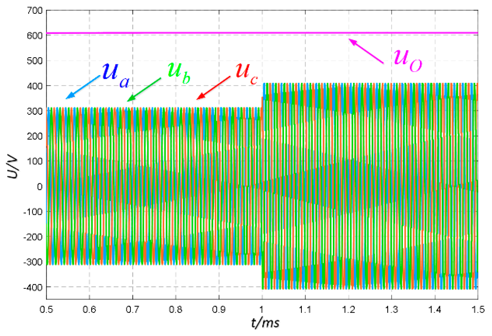
The schematic and its average model of the switching period for the three-phase Vienna rectifier are shown in Figure 1a,b, respectively. In Figure 1a, U o is the output voltage on the DC side and the u x ( x = A , B , C ) is the three-phase input voltage. In the average model shown in Figure 1b, the average voltages U x O ( x = A , B , C ) at nodes A, B, C with respect to the neutral point “O” equal to the phase voltages minus the voltages across the inductors L A , L B , L C (assuming L A = L B = L C = L ), are given by
u x O = u x j ω L i x
where i x ( x = A , B , C ) are inductor currents and ω is line angular frequency.
In the COCC strategy, when the switching frequency is much higher than the line frequency, the voltages across the inductors are usually seen as small enough to be neglected, therefore Equation (2) can be obtained
u x O u x = 2 V i n sin ( ω t K x 120 )
where V i n is the RMS value of the phase voltages and K A = 0 , K B = 1 , K C = 2 . For a three-phase rectifier with unity-power-factor, the control goal is described by
u x = R e i x
where R e = U o R s / ( 2 V m ) is the emulated per-phase resistance when viewed from the ac-input side reflecting the output power-level. The COCC core equations for the three-phase Vienna rectifier are shown below (derivation of Equation (4) and can be found in [20])
V m ( 1 d x ) = | R s i x |
where R s is the equivalent resistance of current sensor and V m = U o R s / 2 R e , d x ( x = A , B , C ) are duty ratio of switches S A , S B and S C , respectively.
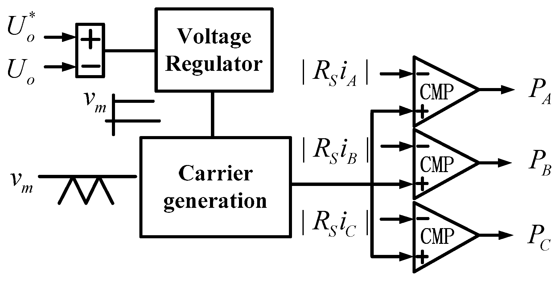
The control block diagram based on COCC core equations is shown in Figure 2. In this control system, the error between the reference voltage and sensed dc-link voltage is regulated through a PI controller, and the output signal V m connects to the carrier generator. The carrier generator synthesizes a triangular waveform with amplitude V m , which is used to compare with the sampled input current signals. PWM signals are then generated to control the three switches in the Vienna rectifier and force the average inductor currents over one switching cycle to follow the corresponding phase voltages. Both digital and analog circuits can achieve the above control goal.
It should be noted that the COCC core Equation (4) is derived based on the assumption of balanced three phase source voltages. In case of unbalanced three phase source voltages, under COCC control, the three phase input currents will follow the vector sum of the positive and negative components of the source voltages to become unbalanced also, and a large capacitance on the DC side is necessary to minimize the input current harmonics and suppress DC side voltage fluctuation [21]. To overcome above problem, [22] proposed a modified OCC, in which a minor modification to COCC is given, by sensing both the source voltages and line currents and reconstructing the reference signals based on harmonic extraction, the three-phase input currents will be improved to become more balanced with sinusoidal waveform, meanwhile the dc-link voltage can still keep on smooth value with smaller ripple. Since the focus of this paper is how to make the power factor of Vienna rectifier become adjustable under OCC control and how to mitigate the input current distortion caused by the current phase shift. For simplicity, all the following discussions are conducted based on the assumption of balanced three phase source voltages.

3. Current Phase-Shift Control Based on MOCC Scheme

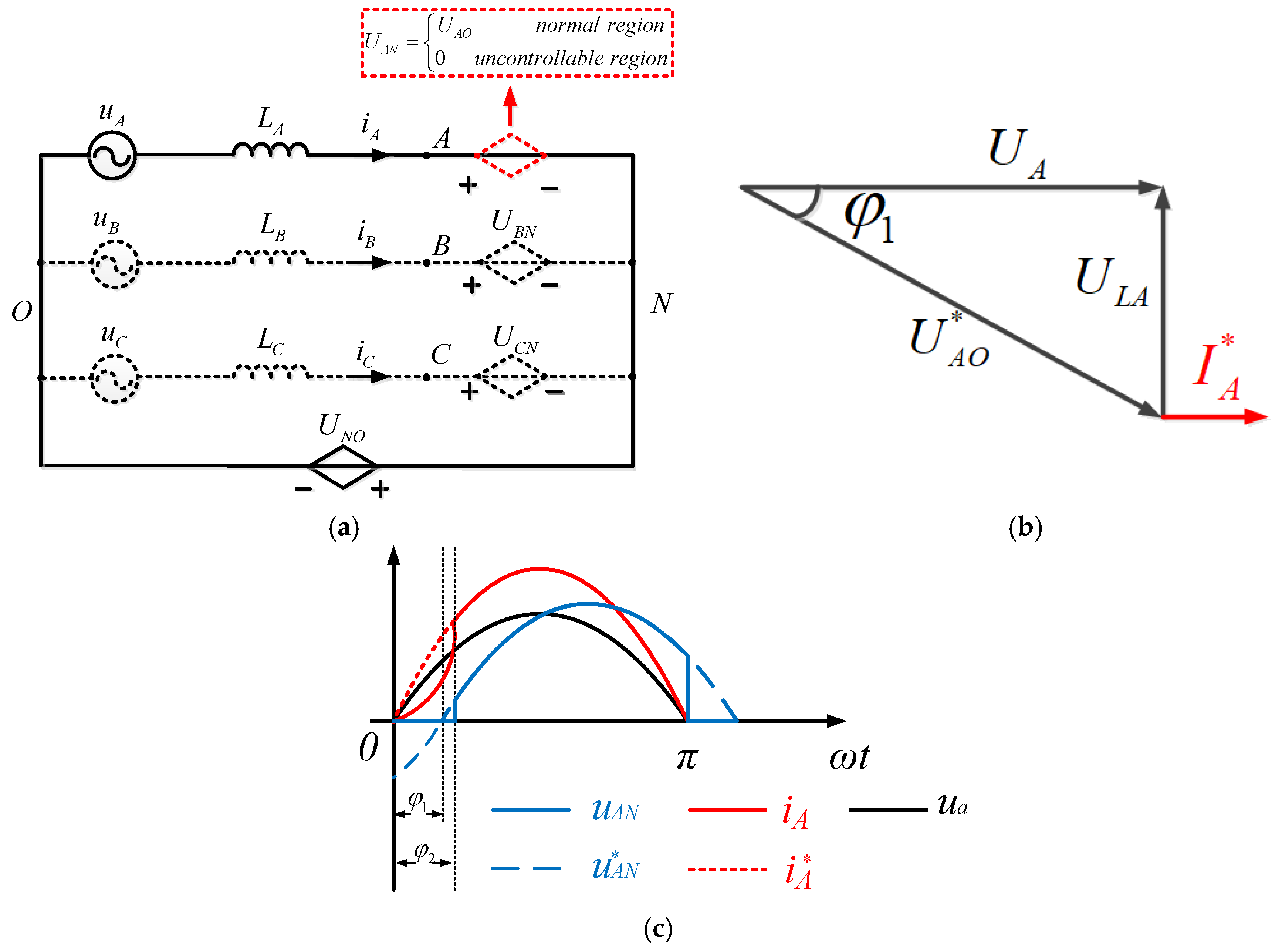
As can be seen from the above description, the essence of the COCC-based three-phase Vienna rectifier is to realize unit power factor operation by resistive load emulation. Figure 3a shows the equivalent circuit for each phase. In this section, the modification to COCC strategy is presented to enable the input power factor of the Vienna rectifier adjustable. To achieve this control goal, the per phase emulated load is changed from a pure resistor R e to a complex impedance Z made up of a resistor R e and a reactor X e in series connection as shown in Figure 3b. X e represents the emulated per-phase reactance reflecting the required output reactive power-level. Figure 3c shows the average model of the switching period for the three-phase Vienna rectifier under MOCC control. The complex impedance of the emulated load Z is given by
Z = R e + j X e

3.1. Input Current Phase-Shift Control Strategy

For a balanced three-phase system, it holds that
u A + u B + u C = 0
The cycle average voltages at nodes A, B, C with respect to the neutral point O are given by
u x O = u x N + u N O     ( x = A , B , C )
Combining Equations (1), (6) and (7) yields
u N O = 1 3 ( u A N + u B N + u C N ) Z 3 ( i A + i B + i C )
In a three-phase three-wire system
i A + i B + i C = 0
Combining Equations (8) and (9) yields
u N O = 1 3 ( u A N + u B N + u C N )
Equation (10) means that different emulated load has no influences to voltage u N O . Substituting Equation (10) into Equation (7) results in
u x j ω L i x = u x N 1 3 ( u A N + u B N + u C N )
Simplifying above equations yields
[ 2 / 3 1 / 3 1 / 3 1 / 3 2 / 3 1 / 3 1 / 3 1 / 3 2 / 3 ] [ u A N u B N u C N ] = [ u A u B u C ] [ j ω L i A j ω L i B j ω L i C ]
If the converter operates in continuous conduction mode (CCM), the average node voltages u A N , u B N , u C N in each switching period can be given by
u x N = U O 2 ( 1 d x ) s i g n ( i x )
s i g n ( i x ) ( x = A , B , C ) is the sign function defined by Equation (14)
s i g n ( i x ) = { 1 , i x 0 1 , i x < 0
Substituting Equation (13) into Equation (12) yields
[ 2 / 3 1 / 3 1 / 3 1 / 3 2 / 3 1 / 3 1 / 3 1 / 3 2 / 3 ] [ ( 1 d A ) s i g n ( i A ) ( 1 d B ) s i g n ( i B ) ( 1 d C ) s i g n ( i C ) ] = 2 U o [ [ u A u B u C ] [ j ω L i A j ω L i B j ω L i C ] ]
As mentioned above, compared to COCC, in MOCC the per phase emulated load is changed from a pure resistor R e to a complex impedance Z , taking this factor into consideration and substituting Equation (5) into Equation (15) yield
[ 2 / 3 1 / 3 1 / 3 1 / 3 2 / 3 1 / 3 1 / 3 1 / 3 2 / 3 ] [ ( 1 d A ) s i g n ( i A ) ( 1 d B ) s i g n ( i B ) ( 1 d C ) s i g n ( i C ) ] = ( R s V m j ( ω L + X e ) R s V m R e ) [ i A i B i C ]
Since the matrix in Equation (16) is singular, there is no unique solution, one possible solution can be obtained in follows
V m ( 1 d x ) = | [ R s j ( ω L + X e ) R s / R e ] i x |
Equation (17) is the core control equation of the MOCC-based three-phase Vienna rectifier. Different from the COCC-based core control Equation (4), two items appear on the right side of Equation (17) instead of only one item, the first item represents the active power consumed by the load, the second item represents the reactive power requirement to the Vienna rectifier which will be used to calculate the phase shift angle of the input current. If the second item of Equation (17) equals to zero, then Equation (17) will be simplified to Equation (4).
If X e = 0 in Equation (17), then Equation (17) will become:
V m ( 1 d x ) = | [ R s ( j ω L R s / R e ) ] i x |
The control strategy based on Equation (18) will enable the Vienna rectifier to operate under unity power factor exactly, which means the displacement angle of input current under the COCC strategy will be regulated to zero. Therefore, Equation (18) can be considered as a more general expression of the OCC core control equation.
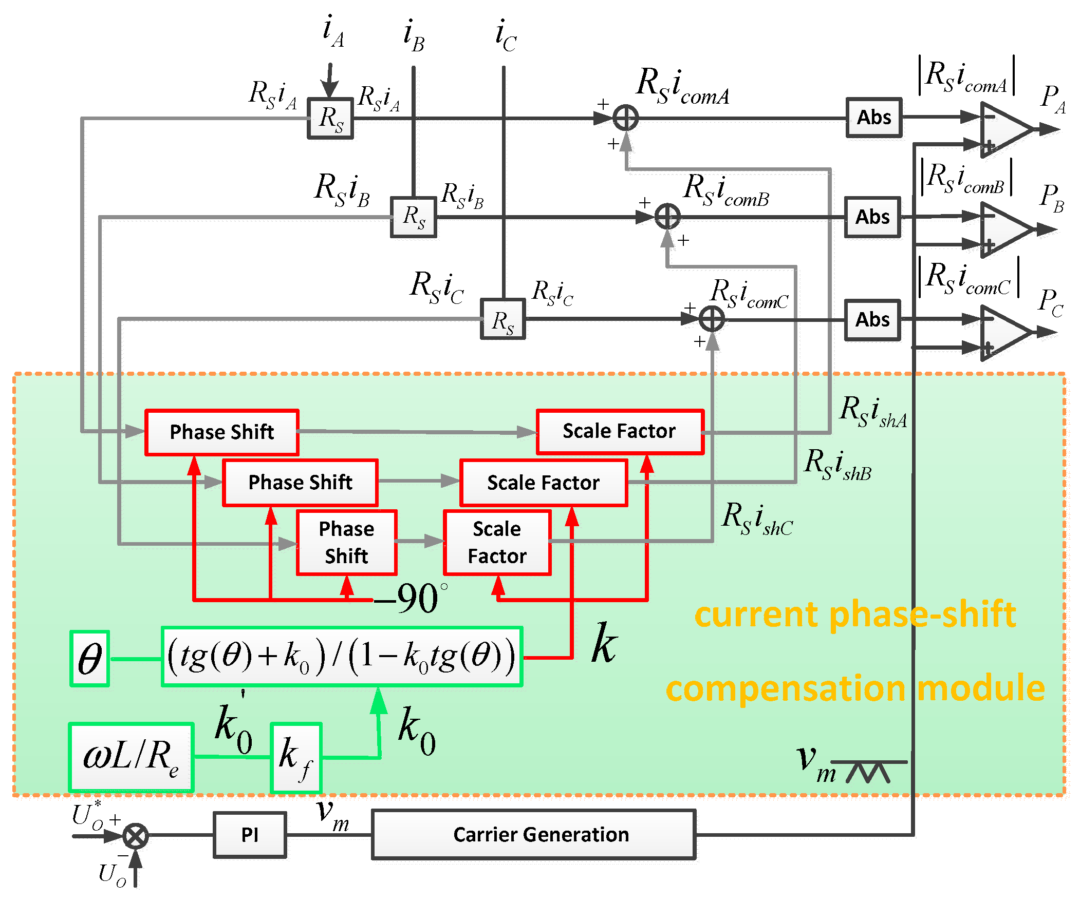
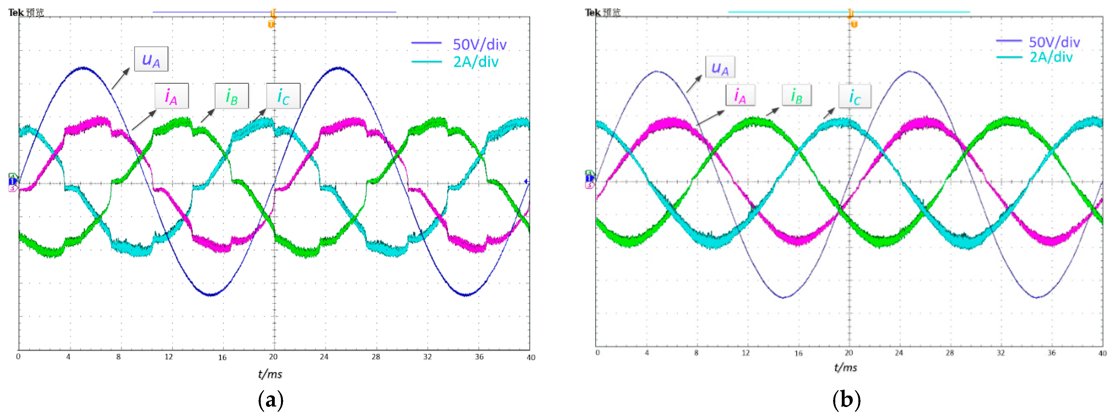
Figure 4 shows the block diagram of the proposed MOCC based control system, a phase shifter block is added which shifts the phase angle of the sensed input current signals R s i x ( x = A , B , C ) by 90° and then multiplies the gain k determined by the requirement of reactive power compensation to generate the shifting current signals R s i s h x ( x = A , B , C ) . Adding the shifting current signals R s i s h x back to the sensed input current signals R s i x gives the compensation current signals R s i c o m x ( x = A , B , C ) , the absolute value of compensation current signals are finally used to compare with the triangular waveforms to generate the PWM signals to force the Vienna rectifier to operate under the required input power factor.

3.2. Implementation of 90° Phase Shift of Input Current Signals

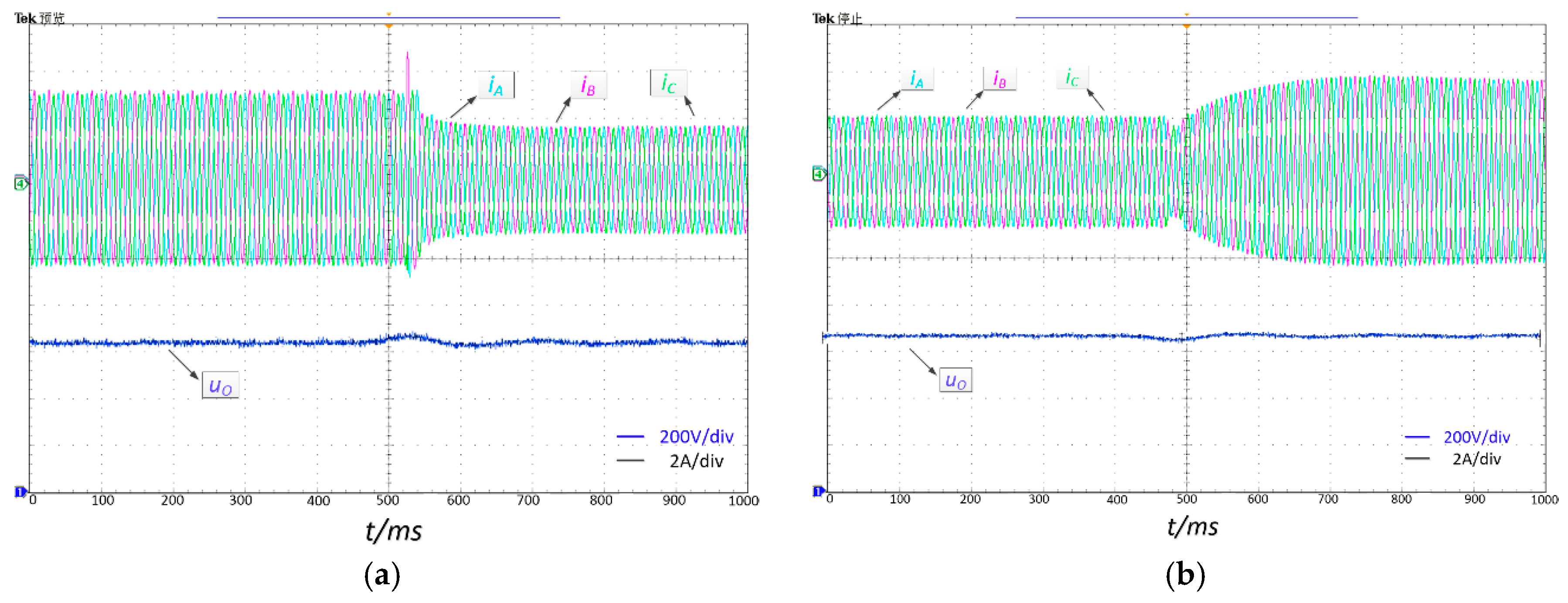
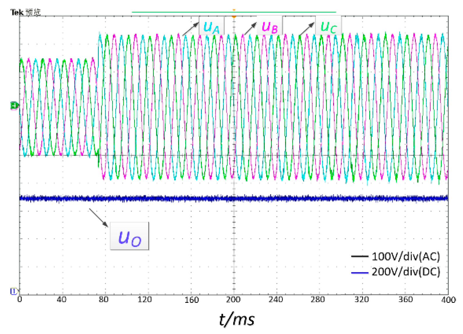
If assuming grid frequency is constant, then one of the simple ways for shifting the phase angle of sensed input current signals by 90° in a digital circuit is to design a stack array with n memory cells, and let n T s = T l / 4 (where T s is the input current sampling period and T l is the fundamental period of input current), thus, after passing through the array, the sampled current signal will naturally lag by a quarter grid cycle. However, grid frequency cannot always remain unchanged, variations in grid frequency will influence the phase shift angle and as a consequence, affect the RPC compensation accuracy, although the allowable range of the grid frequency deviation is usually very limited. In order to reduce the influence of grid frequency, in the phase shifter block of the control system, the number of stack array n is designed to vary with the grid frequency. The value of n is determined by calculating the number of input current samples between two input current zero crossing points. To minimize the impact of errors caused by possible inaccurate zero crossing points determination, and considering that the rate of grid frequency variation is usually much lower than 50 Hz/60 Hz, the multicycle moving average (MCMA) method is adopted, in which, the counter is activated at the zero crossing point in first grid cycle, and stopped at another zero crossing point after q grid cycles, assuming the number of samples between the two zero crossing points is m , then n can be calculated by n = m / 4 q . In the next calculation of n, the number of samples between the zero-crossing point in the second grid cycle and q+1th grid cycle is counted, and so on.

3.3. Calculation of Gain k and Constraints

According to the above discussion, the actual three-phase sensed input current signals R s i x ( x = A , B , C ) under COCC control can be expressed as
R s i x = 2 I i n R s sin ( ω t K x 120 θ z e r o )
where I i n is the RMS value of the input currents, K A = 0 , K B = 1 , K C = 2 and θ z e r o = arctan ( ω L / R e ) is the lagging displacement angle caused by the input inductance voltage drop.
As shown in Figure 4, by shifting the angle of the sensed input current signals R s i x ( x = A , B , C ) by 90°, and multiplies the gain k determined by the required power factor, the shifting current signals R s i s h x ( x = A , B , C ) can be obtained as follows
R s i s h x = 2 k R s I i n sin ( ω t K x 120 90 θ z e r o )
The compensation current signals R s i c o m x ( x = A , B , C ) can then be synthesized as
R s i c o m x = 2 R s I i n 1 + k 2 sin ( ω t K x 120 + θ )
where θ is the displacement angle determined by required input power factor.
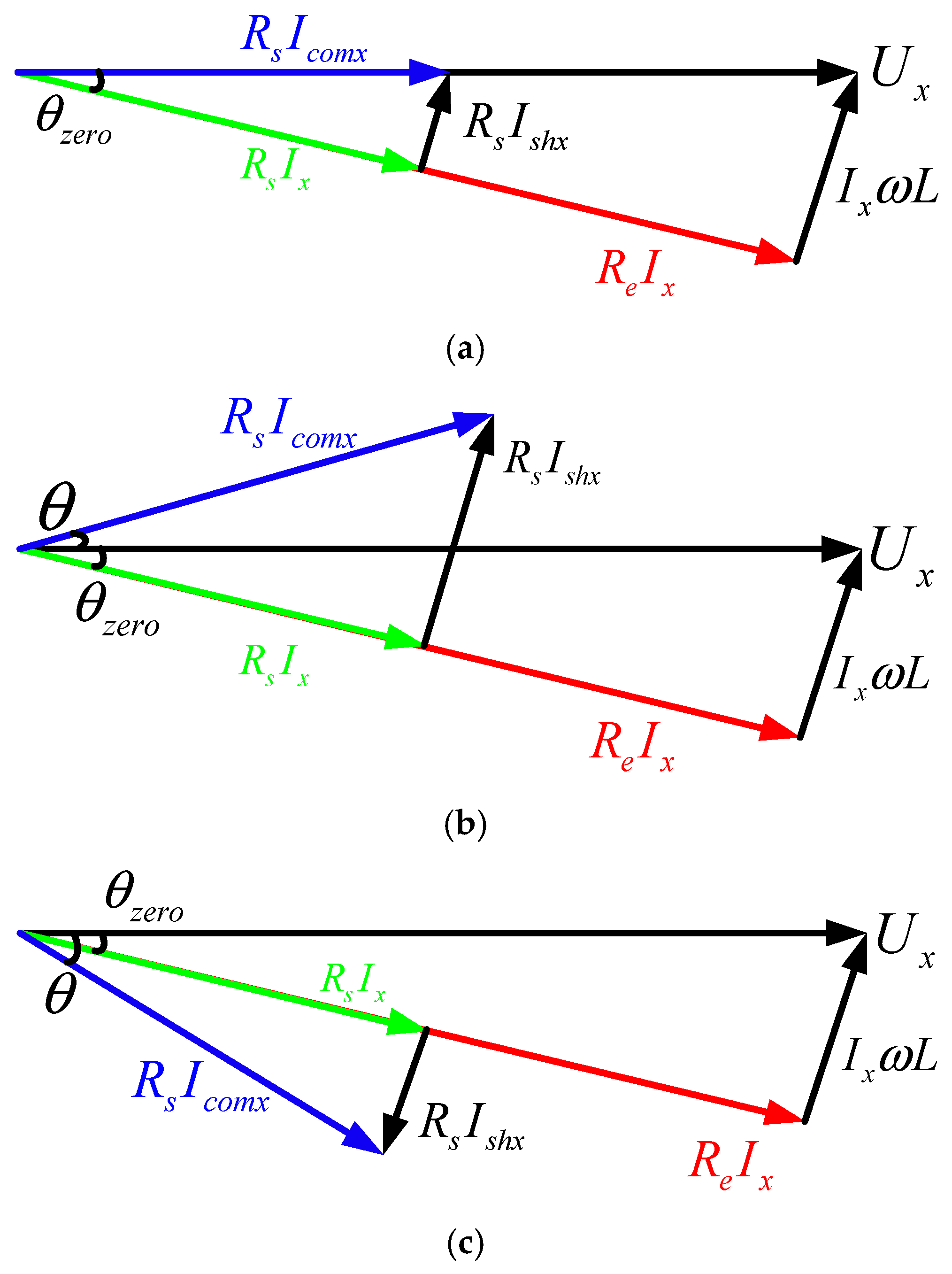
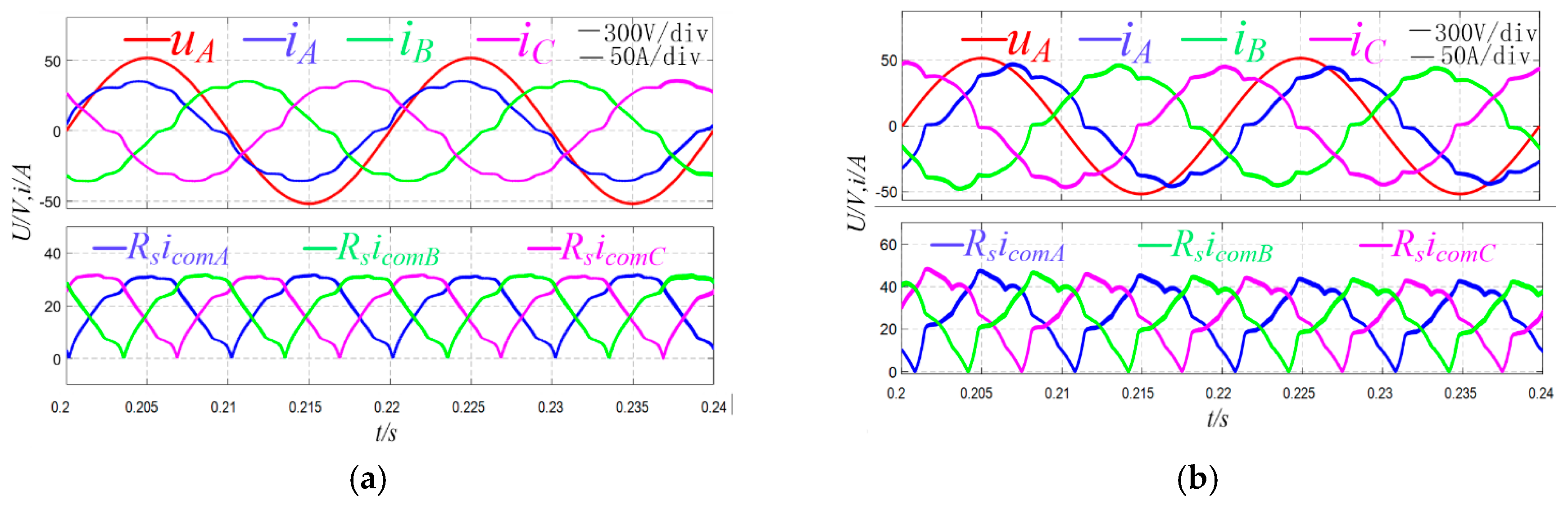
If the rectifier is required to operate under unity power factor as shown in Figure 5a, then k = k 0 = t g ( θ z e r o ) = ω L / R e , in this case, the input inductor voltage drop is compensated, which will enable the rectifier to operate in unity power factor exactly.
If the rectifier is required to operate under leading power factor or under lagging power factor with required displacement angle θ as shown in Figure 5b,c, respectively, then
k = t g ( θ + θ z e r o ) = t g ( θ ) + t g ( θ z e r o ) 1 t g ( θ ) t g ( θ z e r o ) = t g ( θ ) + k 0 1 k 0 t g ( θ )
In Equation (22), θ will take positive value when operating in the leading power factor, while taking negative value when operating in the lagging power factor.
Similar to the above discussion, variations in grid frequency will also affect gain k 0 = ω L / R e , so k 0 should also vary with the grid frequency, to facilitate this, a correction factor k f is provided to the original gain by using above mentioned MCMV method. Supposing that the sampling number between two zero crossing points in an under rated grid frequency ω is m, the corresponding gain is k 0 = ω L / R e , and the sampling number between two zero crossing points under new grid frequency ω 1 is m 1 , then the correction factor k f can be obtained as k f = m / m 1 , the corresponding gain is revised to be k 0 = k f k 0 .
Based on the expressions given by Equations (19), (20) and (21), Equation (17) can be rewritten as
V m ( 1 d x ) = | R s i c o m x |
It can be noted that the expressions of MOCC based on control core Equation (23) and the COCC based control core Equation (4) are very similar.
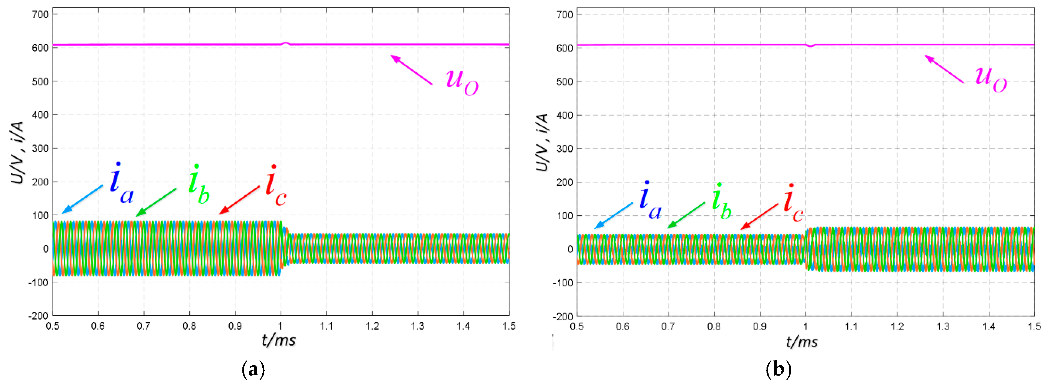
Equation (23) indicates that to ensure the stability of the system, the amplitude of the generated compensation current signals should not exceed the peak value of the triangular waveform V m , otherwise, overmodulation will happen which will make the system become unstable and cause quite a lot of harmonics appearing in the input currents. So, the compensation current signals must meet a constraint given by
2 R s I i n 1 + k 2 V m k V m 2 2 R s I i n 1

4. Input Current Phase-Shift Distortion Mitigation Strategy

4.1. Mechanism of Causing Input Current Distortion

When the MOCC strategy discussed above is applied to a bidirectional rectifier, the rectifier will be able to operate at different power factors while maintaining a sinusoidal input current waveform. However, when the MOCC strategy is applied to a unidirectional rectifier such as Vienna rectifier, due to the characteristic of unidirectional power flow, input current distortion occurs whenever the polarities of the phase current and corresponding node voltage of the rectifier become opposite. This distortion greatly limits the phase-shift control to the input currents. It then follows that the phase voltage and current in phase A under unity power factor operation will be taken as an example to illustrate the mechanism causing input current distortion.
The three phase equivalent circuit of Vienna rectifier based on average model is shown in Figure 6a, Figure 6b shows the ac side phasor diagram of phase A, where U A O * ( = U A N * + U N O * ) and I A * are the reference phase voltage and current in AC side of phase A. When the rectifier operates under unity power factor, the input current I A is required to be in phase with the source voltage U A , the voltage across the input inductor U L A is orthogonal to I A . According to the triangle law of vector addition, U A O lags A by φ 1 as shown in Figure 6b, this lagging angle φ 1 indicates that during the period of φ 1 after the current crosses zero, the input current i A and the ac side voltage u A O are required to have opposite polarities. Note that in normal conditions, u N O is equal to zero and the node voltage u A N ( = u A O ) is utilized to regulate the circuit operating under required power factor. However, due to the unidirectional power flow property, the node voltage u A N and the phase input current i A must always remain in the same polarity. Hence, during the period of φ 2 , the best choice for node voltage u A N is to keep it at zero value [5,23], which makes the input current i A become uncontrollable, if no suitable control is applied in this uncontrollable region, the input current distortion in Phase A will appear as shown in Figure 6c. Furthermore, the distorted i A will further distort the input currents in another two phases at the same time.

4.2. Mitigation Strategy for Input Current Distortion

In this section, based on the MOCC strategy, a method for mitigating or even eliminating the input currents distortion of the three-phase Vienna rectifier through controlling voltage u N O will be studied. Note that u N O is the average voltage of the cycle between node N and node O, which is determined by the average node voltages u A N , u B N and u C N as given by Equation (10).
In following discussion, phase A input current will still be taken as an example, As described above, in normal conditions, phase A input current is controlled by node voltage u A N to operate at the required power factor with sinusoidal waveform. However, in each uncontrollable region in which the input current i A and the reference node voltage u A N * are required to have opposite polarities, u A N will be forced to remain at zero, which makes the conventional control strategy unable to control the actual input current i A to follow the current reference i A * . In this case, Equation (13) can be rewritten as
{ u A N = 0 u B N = ( 1 d b ) s i g n ( i B ) U O / 2 u C N = ( 1 d c ) s i g n ( i C ) U O / 2
Equation (10) is then modified to
u N O = 1 3 ( u B N + u C N )
Substituting Equations (25) and (26) into Equation (7), with help of Equation (23), Equation (27) can be derived as
{ V m ( 1 d b ) = | R s i c o m B | R s i c o m A s i g n ( R s i c o m B ) V m ( 1 d c ) = | R s i c o m C | R s i c o m A s i g n ( R s i c o m C )
The block diagram of the integrated control block based on Equation (27) is shown in Figure 7.
Equation (27) gives further modification to MOCC based control core Equation (17), in which the function of mitigating input current distortion is integrated. It reveals that as long as the MOCC based control law in phase B and phase C follow the rules presented in Equation (27), in each phase A uncontrollable region, the input current of phase A can still follow the sinusoidal reference without any distortion. Equations (28) and (29) give the similar MOCC based control strategy for the phase B uncontrollable region and phase C uncontrollable region, respectively.
{ V m ( 1 d a ) = | R s i c o m A | R s i c o m B s i g n ( R s i c o m A ) V m ( 1 d c ) = | R s i c o m C | R s i c o m B s i g n ( R s i c o m C )
{ V m ( 1 d a ) = | R s i c o m A | R s i c o m C s i g n ( R s i c o m A ) V m ( 1 d b ) = | R s i c o m B | R s i c o m C s i g n ( R s i c o m B )
The second item on the right hand side of Equations (27), (28) and (29) is defined as distortion current signals expressed by R s i d i s x ( x = A , B , C ) , which will be injected into the compensation current signals in each uncontrollable region as shown in Figure 7 to mitigate possible input current distortion. Note that in the uncontrollable regions of phase A, phase B and phase C, the expressions of R s i d i s x are different, for example, in phase A uncontrollable region, R s i d i s C = R s i c o m A / s i g n ( R s i c o m C ) as shown in Equation (27), while in phase B uncontrollable region, R s i d i s C = R s i c o m B / s i g n ( R s i c o m C ) as shown in Equation (28), the expressions of R s i d i s x ( x = A , B , C ) in uncontrollable region of different phases are summarized in Table 1.
In Figure 7 R s i c m d x ( x = A , B , C ) final command current signals are generated by adding distortion current signals to compensation current signals, R s i c m d x will eventually be used to compare with the triangle waveforms to generate the expected PWM pulses to control the Vienna rectifier operating under required power factor with sinusoidal input currents. It should be noted that this proposed MOCC method is applicable to all other three-phase unidirectional star-connected rectifiers.

4.3. Compensation Capacity Analysis

According to above discussion, when phase A compensation current signal gets into the uncontrollable region, the distortion current signals will be injected into the other two-phase compensation current signals which makes the other two phase final command current signals R s i c m d B and R s i c m d C be modified to
{ R S i c m d B ( t ) = | R S i c o m B ( t ) | R S i d i s A ( t ) R S i c m d C ( t ) = | R S i c o m C ( t ) | R S i d i s A ( t )
Similar to above discussion, to ensure the stability of the system, the maximum value of the generated final command current signals cannot exceed the peak value of the triangular waveform, otherwise, overmodulation will happen which will cause increased harmonics appearing in the input currents. So, the final command current signals must also meet the constraint given by
R S i c m d x ( x = A , B , C ) ( t ) V m
From Figure 7, it can be seen that the final command current signals are formed by sensed input current signals R s i x ( x = A , B , C ) (which reflect the active current), shifting current signals R s i s h x ( x = A , B , C ) (which reflect the reactive current), and distortion current signals R s i d i s x ( x = A , B , C ) . Therefore, the maximum displacement angle in leading or lagging (which reflects the maximum reactive power can be provided by the rectifier) is in fact restricted by both the active power consumed by the load and the harmonics of input currents.
Figure 8a,b show the curves of input current total harmonic distortion (THD) at different current phase shift angle and DC load power under COCC control and under MOCC control with current distortion mitigation respectively. If the input current THD is required to be less than 5%, as shown in Figure 8, take the plane defined by THD = 5% to cut the 3D curve, the intersection of the plane and the 3D curve will determine a region, from which the actual operating range of the current phase shifting angle under different load is determined.
Comparing Figure 8a with Figure 8b, it can be easily observed, when MOCC control is used together with current distortion mitigation, the operating range of current phase shifting angle in leading or lagging is significantly extended, which makes the rectifier get much stronger RPC capability.

5. Simulation and Experimental Results

5.1. Compensation Capacity Analysis

In order to verify the effectiveness of the proposed MOCC scheme, simulations are carried out in the MATLAB/Simulink. The main parameters chosen for the simulation models are provided in Table 2.
Figure 9 shows the simulation results under MOCC control with no distortion control strategy applied. Figure 9a shows the waveforms of phase A source voltage, input current and compensation current signal in leading power factor, while Figure 9b shows the similar waveforms in lagging power factor. Unlike the COCC strategy, the signals used to compare with the triangular wave in the MOCC strategy to generate the desired PWM pulse are the absolute value of compensation current signals which are composed of sensed input current signals and shifting current signals. This strategy allows the phase angle of the input current to be varied as required by the control. As shown in the two figures, the phase angle of the input currents is completely determined by the corresponding compensation current signals R S i c o m x ( x = A , B , C ) , and some distortion caused by phase shift occurs periodically in the three input currents of the Vienna rectifier.
Figure 10 shows the simulation results under MOCC control with application of distortion mitigation control strategy. The waveforms of phase A source voltage, three phase input currents and final command current signals in leading power factor with displacement angle θ = 18 ° are shown in Figure 10a. Figure 10b gives the similar waveforms in lagging power factor with displacement angle θ = 33 ° . It should be noted that here the signals used to compare with the triangular wave to generate the desired PWM pulse are changed to the rectified final command current signals. Due to the application of current distortion mitigation control strategy, the distortion of input currents in both modes are suppressed clearly. In Figure 10 it can be observed, some narrow pulses are superimposed on the rectified sinusoidal waveform, which indicates that the distortion current signals are injected periodically to the compensation current signals in each uncontrollable region.
The simulation result of dynamic response of proposed strategy is shown in Figure 11 and Figure 12. In order to verify the stability of the control, the resistance of the load is increased from 30 Ω to 60 Ω at 1 s in Figure 11a and reduced from 30 Ω to 15 Ω at 1 s in Figure 11b. It can be seen from both Figure 11a and Figure 11b the three-phase currents are still operating with the sine waveform and only minor fluctuations appears in the output voltage. In Figure 12, when the input voltage increases from 380 V line-line (L-L) to 500 V(L-L), the DC output voltage continue to keep in stable with no obvious fluctuation, which proves the stability of the proposed control strategy.
The analysis for THD is summarized in Table 3. It can be observed before distortion control strategy is applied, the THD of input current in leading power factor mode is 7.63%, in lagging power factor mode is 7.37%, while after the distortion control strategy is applied, the THD of the input current in leading power factor mode is decreased to 1.32%, in lagging power factor mode it is decreased to 1.44%.The simulation results fully verified the effectiveness of the proposed method for mitigating the possible input current distortion caused by current phase-shift in the unidirectional three-phase Vienna rectifier.
Figure 13 shows the effect of grid frequency variation to the displacement angle of COCC controlled rectifier and MOCC controlled rectifier with and without frequency compensation. The rectifier is required to operate under actual unity power factor, and grid frequency varies from 45 Hz to 55 Hz, it can be observed that the phase lag angle of the grid current under MOCC control is much smaller than that under COCC control, and in the whole range of frequency variation, the displacement angle controlled by MOCC with proposed frequency compensation is kept always near zero.

5.2. Experimental Results

To further verify the performance of the three-phase Vienna rectifier under proposed MOCC scheme, a 1kW down-scaled experiment prototype is built as shown in Figure 14. The parameters of this prototype are provided in Table 4. The rectifier was assembled using three Power MOSFET from IXYS (IXFH46N65X2 46-A 650-V, Infineon, Munich, Germany) and 18 power diodes from Infineon (IDW15E65D2 30-A 650-V, Infineon, Munich, Germany). A TMS320F28335 DSP serves as the core controller. The experimental results are shown in Figure 15, Figure 16, Figure 17 and Figure 18.
First, to verify the performance of regulating power factor of the Vienna rectifier by employing the proposed MOCC scheme, shifting current signals are added to the sensed input current signals, but distortion current signals are not injected. Figure 15 and Figure 16 give the waveforms of phase A source voltage and three-phase input currents in leading power factor with displacement angle θ = 10 ° , and lagging power factor with displacement angle θ = 15 ° , respectively. As is expected, under MOCC control, phase A input current in Figure 15a leads the source voltage, whereas phase A input current in Figure 16a lags the source voltage. However, because the distortion control strategy is not applied, input current distortion appears as shown in both Figure 15a and Figure 16a. To verify the effectiveness of the current distortion control scheme, distortion current signals are injected in each uncontrollable region. Figure 15b and Figure 16b show the corresponding waveforms of three-phase input current and phase A source voltage in leading power factor and lagging power factor respectively. It can be easily observed that the input current distortion in both Figure 15b and Figure 16b are mitigated effectively, the harmonics in the input current are significantly reduced. Moreover, to verify the dynamic characteristics of proposed strategy, the experiment under mutation load and sudden change of input voltage are conducted. As shown in Figure 17 and Figure 18, the resistance of the load is increased from 350 Ω to 600 Ω in Figure 17a and reduced from 350 Ω to 150 Ω in Figure 17b. Three-phase currents are still operating with the sine waveform and the output voltage soon return to stability (within 0.1 s). The input voltage changed from 208 V(L-L) to 350 V (L-L) is shown in Figure 18. It can be observed that the output voltage of the Vienna converter does not fluctuate with the change of input voltage.
To further verify the effectiveness of input current distortion mitigation strategy under MOCC control, the harmonic spectrum analysis to the input current based on the experiment results and the corresponding comparison are carried out. Figure 19a shows the harmonic spectrum for phase A input current operating in leading power factor mode before and after distortion control strategy is enabled. Figure 19b shows the harmonic spectrum for phase A input current operating in lagging power factor mode before and after distortion control strategy is enabled, the corresponding measured THD are also listed in the up right of the two figures.
It can be observed from the two figures, that the input current harmonics under MOCC control are significantly suppressed after the distortion control strategy is enabled. In leading power factor mode, before the distortion control strategy is enabled, the THD of the input current under the MOCC is 11.06%, while the THD of the input current drops to 5.15% after distortion control strategy is enabled. In lagging power factor mode, before distortion control strategy is enabled, the THD of input current under the MOCC is 17.64%, while the THD of input current drops to 5.07% after distortion control strategy is enabled. The input power factor and the efficiency in four different control modes are also calculated based on the experiment results and summarized in Table 5 and Table 6.

6. Conclusions

In this paper, a modified OCC strategy is proposed in order to incorporate the reactive power compensation functionality into the three-phase Vienna rectifier. Compared with the conventional OCC strategy, the core control equation of the MOCC is established based on the input complex impedance emulation. Thus, the input power factor of the three-phase Vienna rectifier becomes adjustable. In order to compensate the input current distortion caused by current phase shift, a method for mitigating current distortion is also provided to compensate the possible input current distortion caused by input current phase shift. This strategy will periodically inject the corresponding distortion current signals into the compensation current signals in each uncontrollable region. Moreover, the constraints on the maximum value of the displacement angle in leading or lagging are also discussed, which can be used to determine the maximum reactive power that the three-phase Vienna rectifier can provide. The MOCC scheme proposed by this paper applies to all other rectifiers (bidirectional or unidirectional) and the proposed control method for mitigating input current distortion is applicable to all other three-phase star-connected unidirectional rectifiers as well. The validity and feasibility of the proposed MOCC schemes are fully verified by simulations and experimental results from a 1 kW three-phase Vienna rectifier prototype.

Author Contributions

J.L. and C.W. designed the research; H.C., Y.Z. and Z.Z. finished and collected the experiment and data.

Funding

This research was funded by the National Natural Science Foundation of China grant number 51577187 and The Fundamental Research Funds for the Central Universities grant number 2015QJ11.

Acknowledgments

This work was supported by the National Natural Science Foundation of China under Grant No. 51577187 and The Fundamental Research Funds for the Central Universities (2015QJ11).

Conflicts of Interest

The authors declare no conflict of interest.

References

  1. Singh, M.; Khadkikar, V.; Chandra, A.; Varma, R.K. Grid Interconnection of Renewable Energy Sources at the Distribution Level With Power-Quality Improvement Features. IEEE Trans. Power Deliv. 2011, 26, 307–315. [Google Scholar] [CrossRef]
  2. Kisacikoglu, M.C.; Ozpineci, B.; Tolbert, L.M. EV/PHEV Bidirectional Charger Assessment for V2G Reactive Power Operation. IEEE Trans. Power Electron. 2013, 28, 5717–5727. [Google Scholar] [CrossRef]
  3. Hu, K.W.; Liaw, C.M. On a Bidirectional Adapter With G2B Charging and B2X Emergency Discharging Functions. IEEE Trans. Ind. Electron. 2014, 61, 243–257. [Google Scholar] [CrossRef]
  4. Park, S.M.; Park, S.Y. Versatile unidirectional AC-DC converter with harmonic current and reactive power compensation for smart grid applications. In Proceedings of the IEEE Applied Power Electronics Conference and Exposition, Fort Worth, TX, USA, 16–20 March 2014; pp. 2163–2170. [Google Scholar]
  5. Park, S.M.; Park, S.Y. Versatile Control of Unidirectional AC–DC Boost Converters for Power Quality Mitigation. IEEE Trans. Power Electron. 2015, 30, 4738–4749. [Google Scholar] [CrossRef]
  6. Alahuhtala, J.; Virtakoivu, J.; Viitanen, T.; Routimo, M.; Tuusa, H. Space Vector Modulated and Vector Controlled Vienna I Rectifier with Active Filter Function. In Proceedings of the 2007 Power Conversion Conference - Nagoya, Nagoya, Japan, 2–5 April 2007; pp. 62–68. [Google Scholar]
  7. Kedjar, B.; Al-Haddad, K. Three-phase four-wire Vienna I rectifier with active filter function including neutral current mitigation. In Proceedings of the IEEE International Symposium on Industrial Electronics, Seoul, Korea, 5–8 July 2009; pp. 1510–1515. [Google Scholar]
  8. Kedjar, B.; Kanaan, H.Y.; Al-Haddad, K. Vienna Rectifier with Power Quality Added Function. IEEE Trans. Ind. Electron. 2014, 61, 3847–3856. [Google Scholar] [CrossRef]
  9. Wang, C.; Zhuang, Y.; Jiao, J.; Zhang, H.; Wang, C.; Cheng, H. Topologies and Control Strategies of Cascaded Bridgeless Multilevel Rectifiers. IEEE J. Emerg. Sel. Top. Power Electron. 2017, 5, 432–444. [Google Scholar] [CrossRef]
  10. Ahmed, M.; Kuisma, M.; Tolsa, K.; Silventoinen, P. Implementing sliding mode control for buck converter. In Proceedings of the IEEE 34th Annual Power Electronics Specialist Conference, Acapulco, Mexico, 15–19 June 2003; pp. 634–637. [Google Scholar]
  11. Ma, D.S.; Ki, W.H.; Tsui, C.Y. An integrated one-cycle control buck converter with adaptive output and dual loops for output error correction. IEEE J. Solid-State Circuits 2004, 39, 140–149. [Google Scholar] [CrossRef]
  12. Abramovitz, A.; Tayar, T.; Shmilovitz, D. Modified OCC DCM boost PFC rectifier. In Proceedings of the 19th European Conference on Power Electronics and Applications (EPE’17 ECCE Europe), Warsaw, Poland, 11–14 September 2017; pp. 1–7. [Google Scholar]
  13. Bagawade, S.; Jain, P. Interleaved boost based AC/DC bidirectional converter with four quadrant power control based on one-cycle controller (OCC). In Proceedings of the IEEE Applied Power Electronics Conference and Exposition (APEC), Long Beach, CA, USA, 20–24 March 2016; pp. 544–551. [Google Scholar]
  14. Qiao, C.M.; Smedley, K.M.; Maddaleno, F. A single-phase active power filter with one-cycle control under unipolar operation. IEEE Trans. Circuits Syst. Regul. Pap. 2004, 51, 1623–1630. [Google Scholar] [CrossRef]
  15. Tang, Y.; Loh, P.C.; Wang, P.; Choo, F.H. One-Cycle-Controlled Three-Phase PWM Rectifiers With Improved Regulation Under Unbalanced and Distorted Input-Voltage Conditions. IEEE Trans. Power Electron. 2010, 25, 2786–2796. [Google Scholar] [CrossRef]
  16. Smedley, K.M.; Cuk, S. One-cycle control of switching converters. In Proceedings of the IEEE Annual Power Electronics Specialists Conference, Cambridge, MA, USA, 24–27 June 1991; pp. 888–896. [Google Scholar]
  17. Mao, A.P.; Xie, B.S.; Jia, C.H.; Zhang, D.Y.; Xu, E.J. Analysis and improvement on input characteristics of VIENNA converter with inductive filter and one-cycle-control method. In Proceedings of the 9th International Conference on Power Electronics and ECCE Asia (ICPE-ECCE Asia), Seoul, Korea, 1–5 June 2015; pp. 2706–2711. [Google Scholar]
  18. Mao, P.; Xie, S.; Xu, A.; Xu, Z. Current phase lag issue and the compensation scheme for OCC PFC converter. In Proceedings of the IEEE 6th International Power Electronics and Motion Control Conference, Wuhan, China, 17–20 May 2009; pp. 1678–1683. [Google Scholar]
  19. Wang, C.; Liu, J.; Cheng, H. One-Cycle Control Based Vienna Rectifiers with Input Power Factor Regulation. In Proceedings of the 3rd International Conference on Insulating Materials, Material Application and Electrical Engineering, Melbourne, Australia, 15–16 September 2018. [Google Scholar]
  20. Qiao, C.M.; Smedley, K.M. Three-phase unity-power-factor star-connected switch (VIENNA) rectifier with unified constant-frequency integration control. IEEE Trans. Power Electron. 2003, 18, 952–957. [Google Scholar] [CrossRef]
  21. Jin, T.; Smedley, K.M. Operation of One-Cycle Controlled Three-Phase Active Power Filter With Unbalanced Source and Load. IEEE Trans. Power Electron. 2006, 21, 1403–1412. [Google Scholar] [CrossRef]
  22. Tang, Y.; Loh, P.C.; Wang, P.; Choo, F.H. One-cycle controlled three-phase PWM rectifiers with improved regulation under unbalanced and distorted input voltage conditions. In Proceedings of the International Conference on Power Electronics and Drive Systems, Taipei, Taiwan, 2–5 November 2009; pp. 579–584. [Google Scholar]
  23. Liu, J.; Liu, Y.; Zhuang, Y.; Wang, C. Analysis to Input Current Zero Crossing Distortion of Bridgeless Rectifier Operating under Different Power Factors. Energies 2018, 11, 2447. [Google Scholar] [CrossRef]
Figure 1. (a) A three-phase VIENNA rectifier and (b) its average model of switching period.
Energies 12 03375 g001
Figure 2. Conventional one-cycle-control (COCC) based control block diagram.
Energies 12 03375 g002
Figure 3. (a) COCC based per phase equivalent circuit of Vienna rectifier, (b) modified one-cycle-control (MOCC) based per phase equivalent circuit of Vienna rectifier and (c) MOCC based average model of switching period for three-phase Vienna rectifier.
Energies 12 03375 g003
Figure 4. MOCC based control block diagram with current phase-shift control strategy.
Energies 12 03375 g004
Figure 5. Phasor diagram of per phase voltage and current (a) under unity power factor (b) under leading power factor (c) under lagging power factor.
Energies 12 03375 g005
Figure 6. (a) Equivalent circuit diagram of three-phase Vienna rectifier (b) phasor diagram of phase A voltage and current under unity power factor (c) expected waveforms and actual waveforms of phase A voltage and current.
Energies 12 03375 g006
Figure 7. Block diagram of whole control system of phase A based on Equation (27).
Energies 12 03375 g007
Figure 8. Input current THD varied with current phase shifting angle and DC load power. (a) under COCC. (b) under MOCC with current distortion mitigation.
Energies 12 03375 g008
Figure 9. MOCC based phase A source voltage and three-phase input current waveforms and the rectified compensation current signals R s i c o m x without distortion control strategy applied. (a) Leading power factor. (b) Lagging power factor.
Energies 12 03375 g009
Figure 10. MOCC based phase A source voltage and three-phase input current waveforms as well as the rectified final command current signal R S i c m d x ( x = A , B , C ) with application of a distortion control strategy. (a) Under leading power factor. (b) Under lagging power factor.
Energies 12 03375 g010
Figure 11. Input three-phase current and output voltage waveform at variation of load (a) The resistance of the load is increased from 30 Ω to 60 Ω. (b) The resistance of the load is reduced from 30 Ω to 15 Ω.
Energies 12 03375 g011
Figure 12. Input three-phase voltage and output voltage waveform at variation of input voltage.
Energies 12 03375 g012
Figure 13. Effect of grid frequency variation to the displacement angle of COCC controlled rectifier and MOCC controlled rectifier with and without frequency compensation.
Energies 12 03375 g013
Figure 14. Down-scaled experiment prototype.
Energies 12 03375 g014
Figure 15. MOCC based three-phase input currents and phase A source voltage in leading power factor (a) without distortion mitigation control, (b) with distortion mitigation control.
Energies 12 03375 g015
Figure 16. MOCC based three-phase input currents and phase A source voltage in lagging power factor (a) without distortion mitigation control, (b) with distortion mitigation control.
Energies 12 03375 g016
Figure 17. MOCC based three-phase input currents and phase output voltage at variation of load (a) the resistance of the load is increased from 350 Ω to 600 Ω (b) the resistance of the load is reduced from 350 Ω to 150 Ω.
Energies 12 03375 g017
Figure 18. Input three-phase voltage and output voltage waveform at variation of input voltage.
Energies 12 03375 g018
Figure 19. Comparison results of phase A input current THD under MOCC control with and without distortion mitigation control (a)under leading power factor. (b)under lagging power factor.
Energies 12 03375 g019
Table 1. Expressions of R s i d i s x ( x = A , B , C ) in uncontrollable regions of different phases.
Uncontrollable RegionPhase APhase BPhase C
R s i d i s A - R s i c o m B s i g n ( R s i c o m A ) R s i c o m C s i g n ( R s i c o m A )
R s i d i s B R s i c o m A s i g n ( R s i c o m B ) - R s i c o m C s i g n ( R s i c o m B )
R s i d i s C R s i c o m A s i g n ( R s i c o m C ) R s i c o m B s i g n ( R s i c o m C ) -
Table 2. Simulation Parameters.
ParameterValue
Input line-line voltage380 V
Input inductance2.6 mH
Switching frequency20 kHz
Load resistance30 Ω
Source voltage frequency50 Hz
DC-link capacitors5000 μF
DC-link voltage700 V
Table 3. Input current THD comparison with and without distortion mitigation.
Displacement AngleMOCC without Distortion MitigationMOCC with Distortion Mitigation
θ = 18 ° 7.63%1.32%
θ = 33 ° 7.37%1.44%
Table 4. Experimental parameters.
ParameterValue
Input line-line voltage208 V
Input inductance3 mH
Switching frequency50 kHz
Load resistance350 Ω
Source voltage frequency50 Hz
DC-link capacitors705 μF
DC-link voltage600 V
Table 5. Power factor in different situations.
Displacement AngleMOCC without Distortion MitigationMOCC with Distortion Mitigation
θ = 10 ° 0.87590.9340
θ = 15 ° 0.79650.9172
Table 6. Efficiency in different situations.
Displacement AngleMOCC without Distortion MitigationMOCC with Distortion Mitigation
θ = 10 ° 98.38%98.62%
θ = 15 ° 98.27%98.57%

