Mitigation of Common Mode Voltage Issues in Electric Vehicle Drive Systems by Means of an Alternative AC-Decoupling Power Converter Topology


Abstract
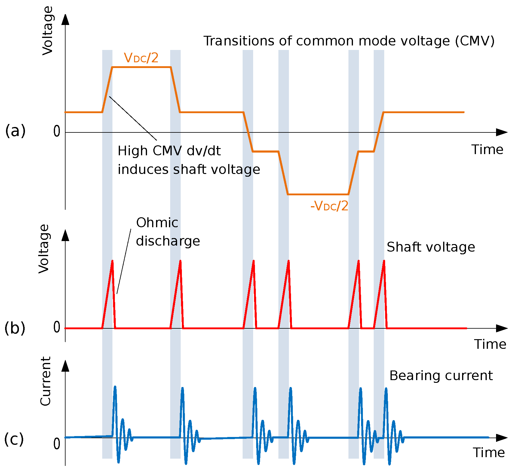
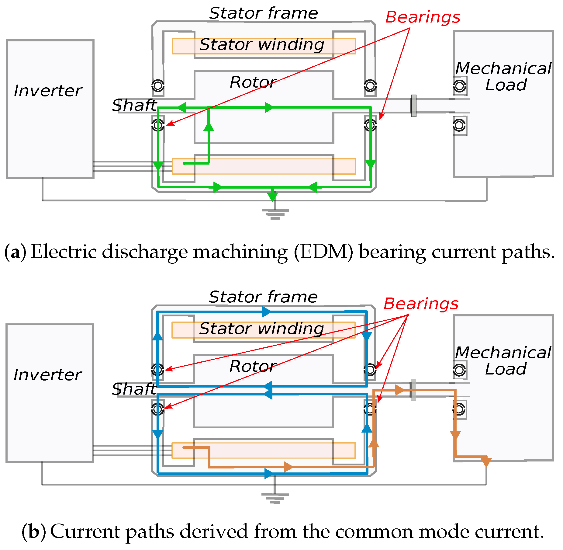
1. Introduction
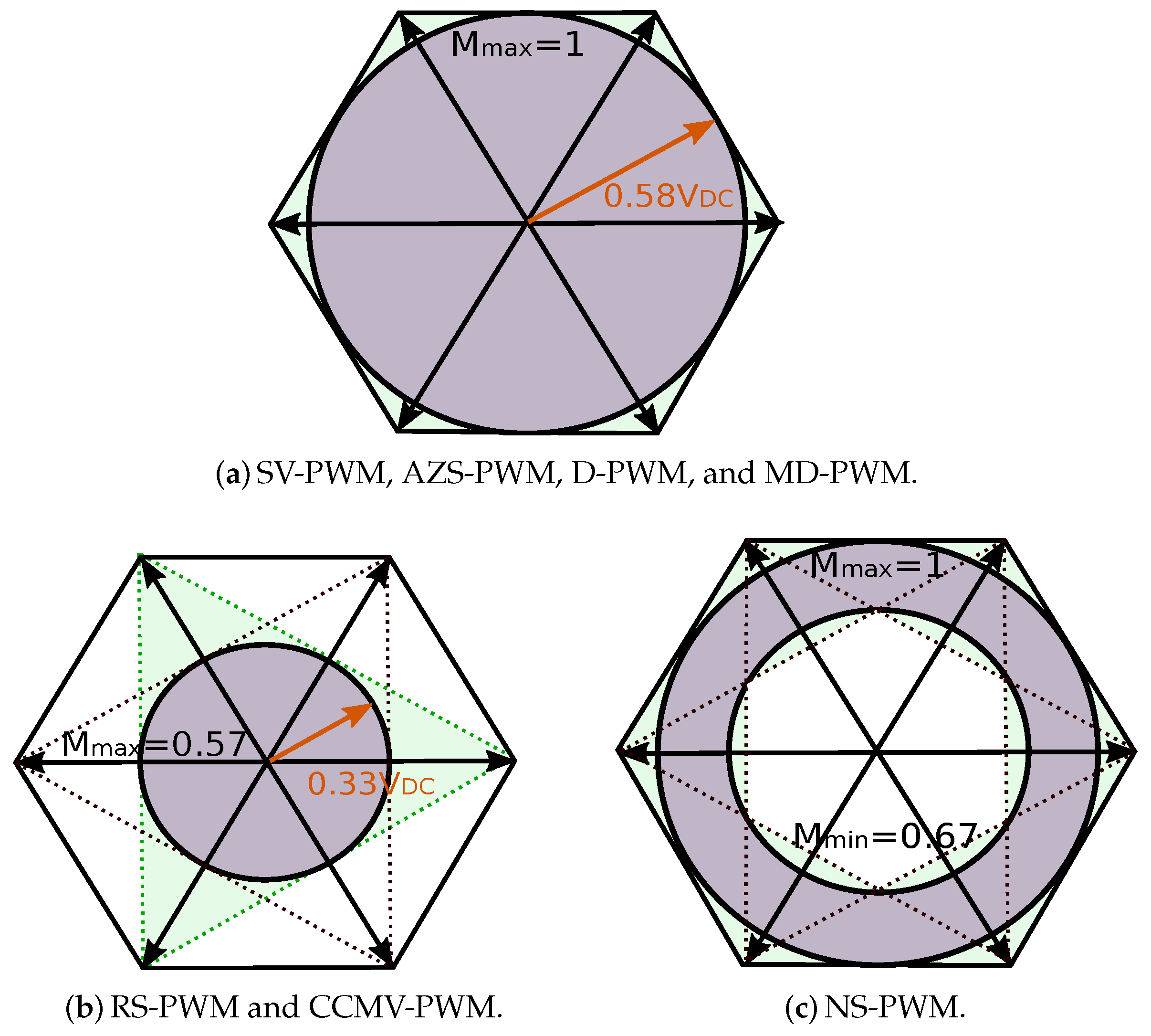
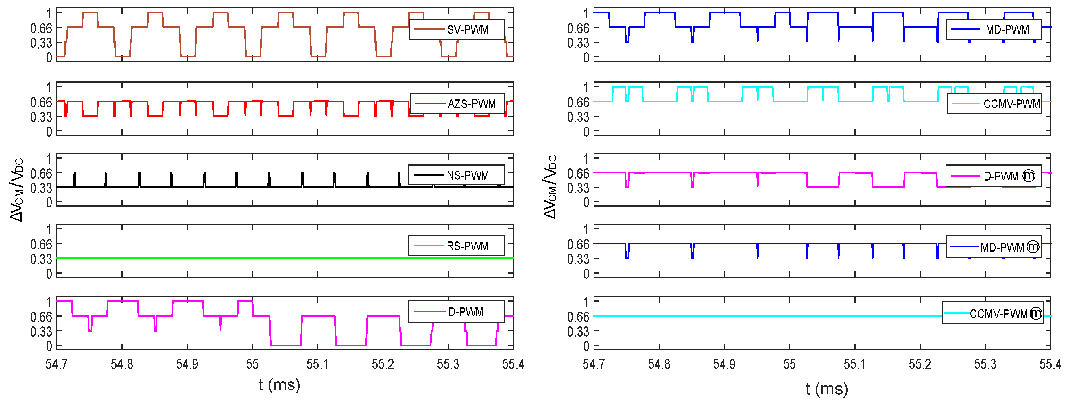
2. Conventional and CMV Mitigation Modulation Techniques for Two-Level Three-Phase Inverters
 ”.).
”.).3. Topologies for CMV Reduction
3.1. State-of-the-Art of Three-Phase Decoupling Topologies
- (a)
- H7: This topology is a derivative of the H5 architecture. The single-phase H5 topology was originally developed for non-isolated photovoltaic applications, and it has been a subject of study in the recent scientific literature. From this topology, various authors have proposed a three-phase extension (Figure 5a), known as H7 [25,37]. As in the H5, this architecture tries to reduce the CMV by including an additional switch. The disadvantage of this topology is that it does not use a clamping diode to control the CMV level.
- (b)
- H8: The H8 topology (Figure 5b) has its origin in the single-phase H6 topology. The difference from the traditional VSI is that incorporates two active DC-decoupling switches that are activated when the zero voltage vectors are applied [25,26,41,42]. This topology reduces the CMV to a greater extent than H7, but as it uses more devices, the power losses increase.
- (c)
- H8D2: This is a variant of the H8 topology (Figure 5c). This is constituted by a voltage divider, constituted by three balanced capacitors and two clamping diodes, placed between the two intermediate points of the voltage divider. This allows establishing the desired CMV during the zero voltage states [21,42,43]. However, as the H8, the greater number of devices increases the losses.
- (d)
- oH7: This topology (Figure 5d) is not as wide-spread as the others. It has one more clamping device than the H7 topology, and it is a modification of the single-phase oH5 topology [42]. However, the additional complexity of oH7 does not justify the benefits of this topology, as the utilization of only one controllable device is sufficient in the voltage divider to provide the desired CMV level.
- (a)
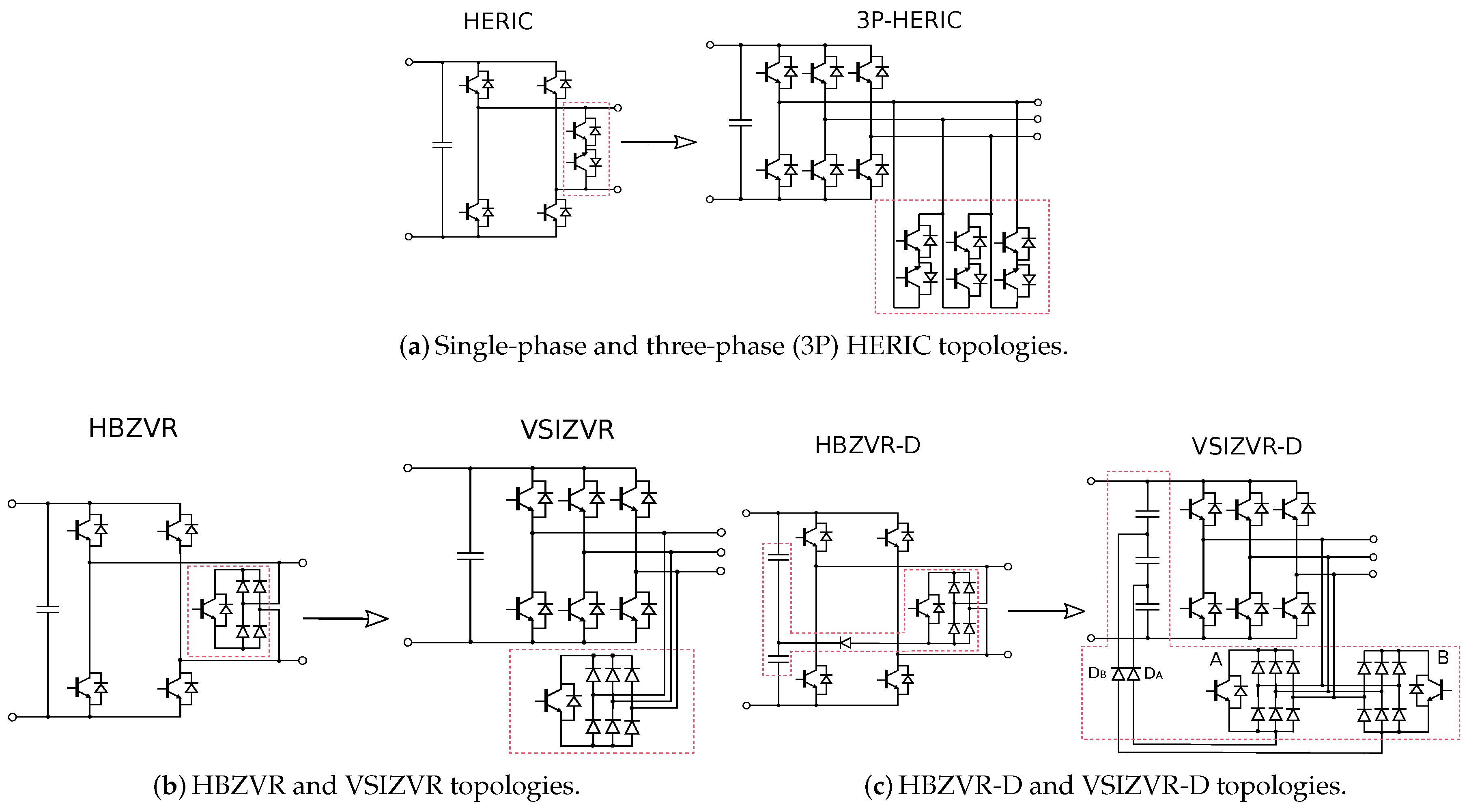
- 3P-HERIC: The best-known AC-decoupling single-phase topology is the high efficient and reliable inverter concept (HERIC) converter [32,33,34,35]. However, the three-phase conversion derivative of this topology, named 3P-HERIC (Figure 6a), is not found in the literature, because it can be considered as complex due to the excessive number of additional active devices required for its implementation.
- (b)
- VSIZVR: In [44], a new topology based on the extension of the H-bridge zero-voltage state rectifier (HBZVR) configuration was presented (Figure 6b). This topology, named the VSI zero-voltage state rectifier (VSIZVR), incorporates one rectifier circuit to reduce the CMV. However, as the H7 alternative, this topology is not very attractive, because it does not use the clamping method to control the voltage.
- (c)
- VSIZVR-D: Similar to the previous topology, another variant of the HBZVR-D converter was presented in [45] (Figure 6c). This topology, named the VSI zero-voltage state rectifier with clamping diodes (VSIZVR-D), incorporates two rectifier circuits connected to the DC bus by means of two clamping diodes. The drawback of this topology is that the B-rectifier clamping voltage level cannot be controlled.
3.2. Other Three-Phase DC and AC-Decoupling Topologies
- (a)
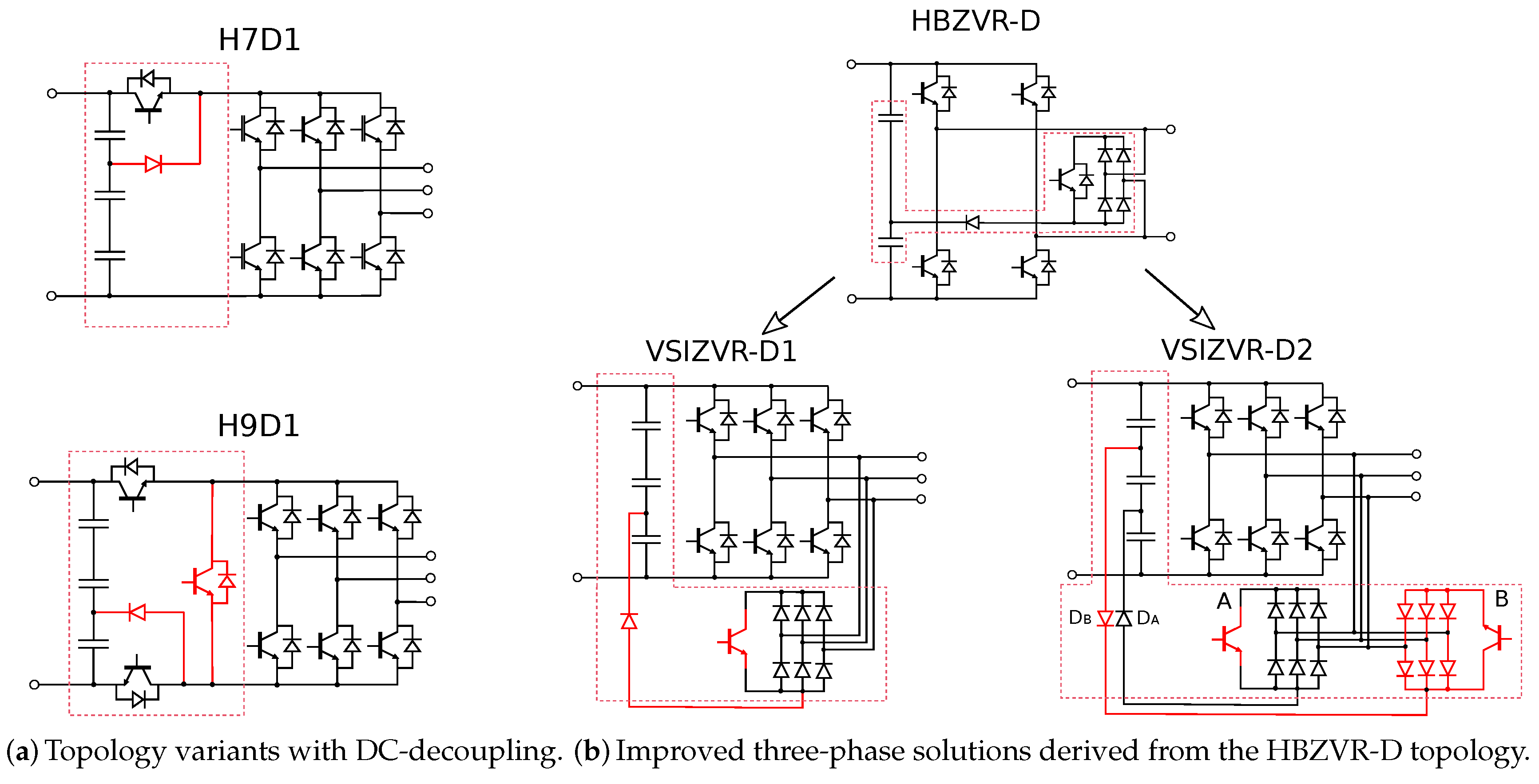
- H7D1: A proposed alternative to the H7 topology, named H7D1, is shown in Figure 7a. Unlike the oH7 topology, it uses a clamping diode to set the CMV to controllable values (portion of the DC bus voltage), which can be considered as a significant advantage.
- (b)
- H9D1: This alternative (Figure 7a) is the only one that has not been derived from a single-phase configuration. The objective of this topology is to improve CMV without incorporating additional AC-decoupling diodes and using only the VSI diodes. In order to achieve this goal, all the devices are opened during the application of zero vectors. For that reason, it is mandatory to incorporate a DC-decoupling mechanism as in the H8 configuration. However, the simultaneous use of DC-decoupling and AC-decoupling will significantly increase the losses of the converter. That is the reason why this alternative is not attractive for EV applications.
- (c)
- VSIZVR-D1: The VSIZVR topology (Figure 6b) has the limitation of not being able to control the CMV during the application of zero vectors. An improved topology that includes a clamping diode to provide the desired voltage level, named the VSI zero-voltage state rectifier with one clamping diode (VSIZVR-D1), can be seen in Figure 7b. Unlike the H9D1 variant, this topology achieves the same CMV without using the DC-decoupling solution, but adding a diode rectifier bridge. In addition, it is not necessary to use the rectifier bridge switch anti-parallel diode, because the current does not flow through it.
- (d)
- VSIZVR-D2: As stated before, the topology shown in Figure 6c has a significant drawback, as the B-rectifier clamping voltage level cannot be controlled, achieving the same result as in the VSIZVR-D1 topology (Figure 7b). Another alternative (Figure 7b), named VSIZVR-D2, incorporates two rectifier circuits properly connected to the DC bus by means of two clamping diodes. Due to the advantages offered by this topology, its operation principles will be thoroughly explained in Section 3.3.
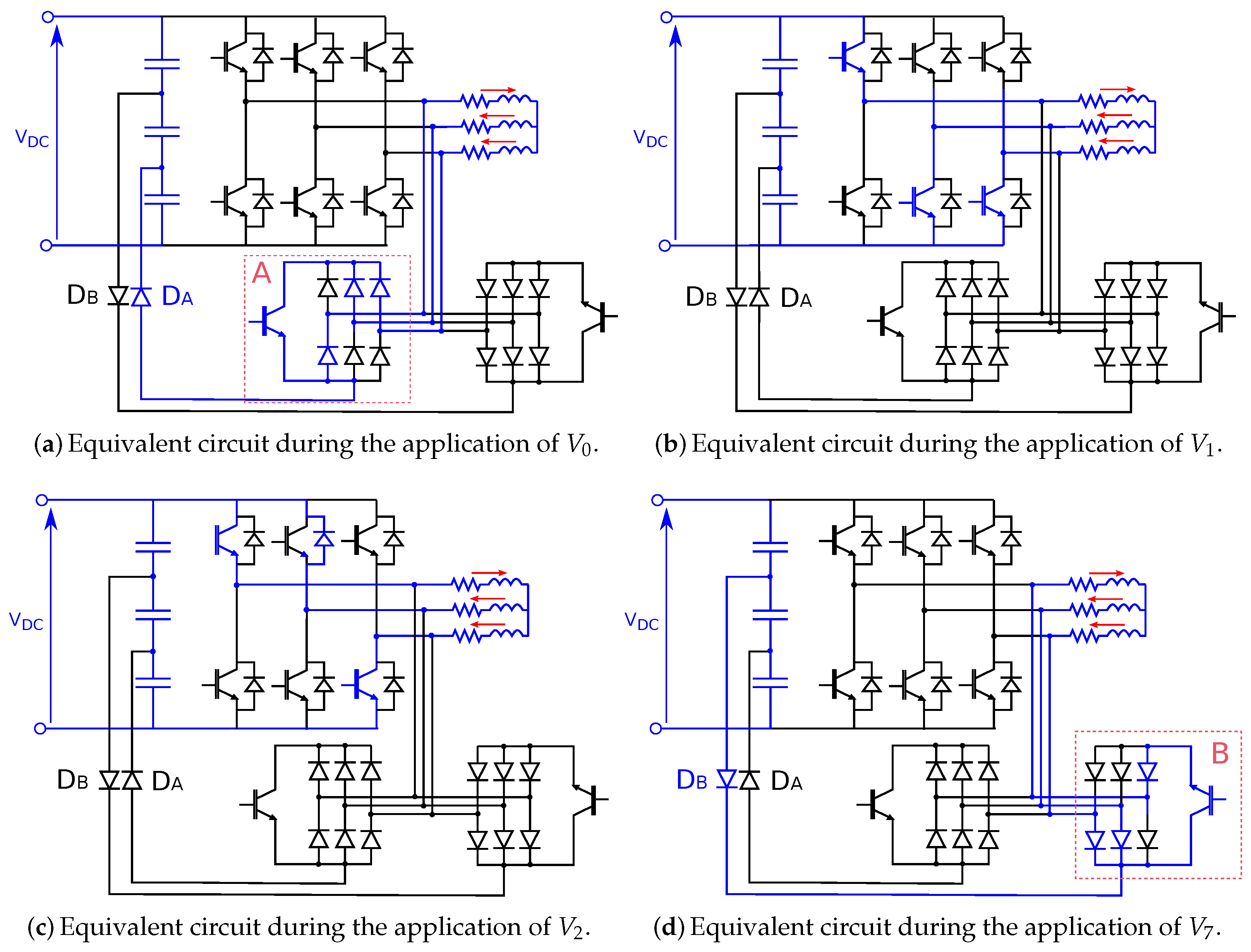
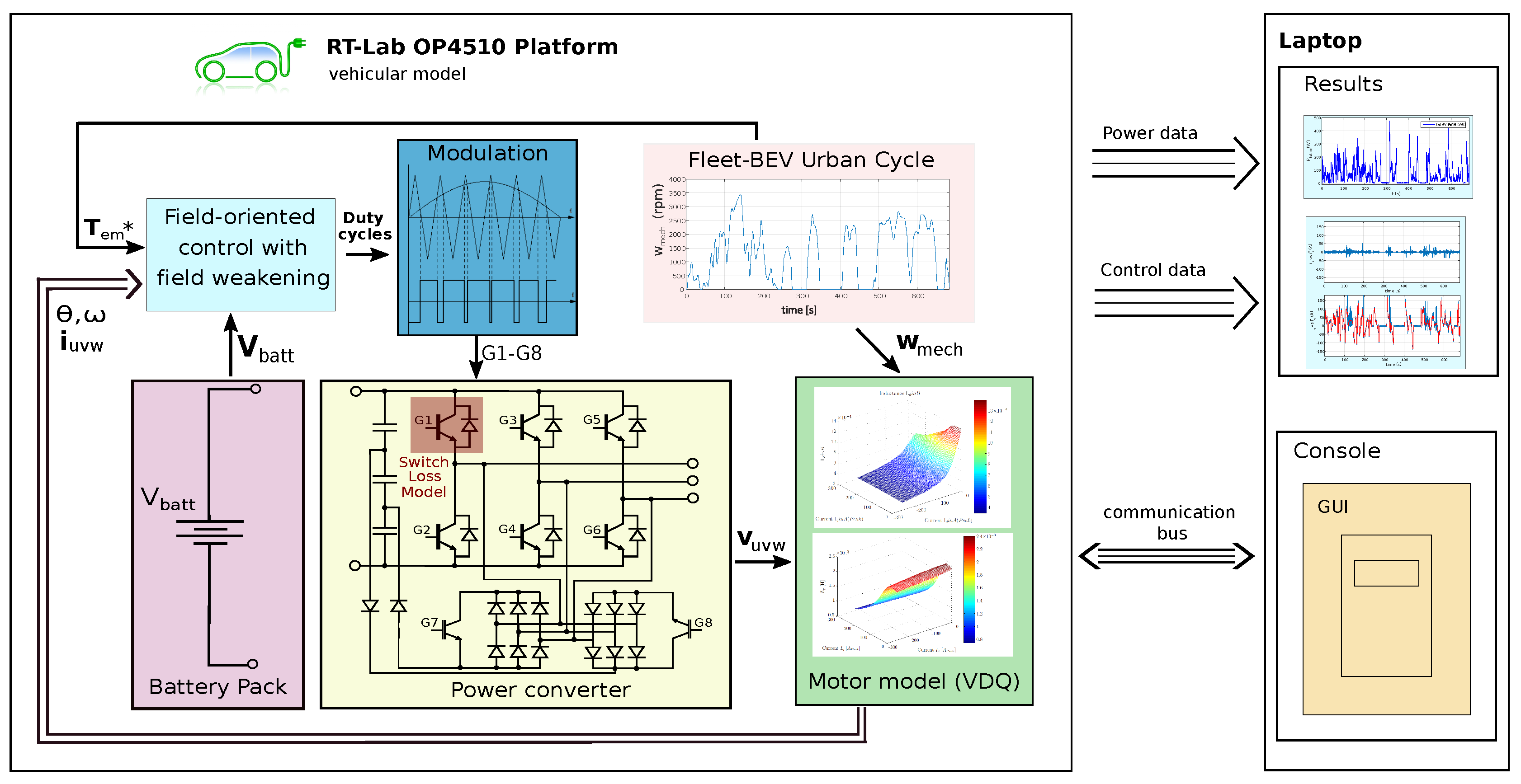
3.3. Operation Principles of the VSIZVR-D2 Topology
4. Analysis of the CMV Reduction Topologies
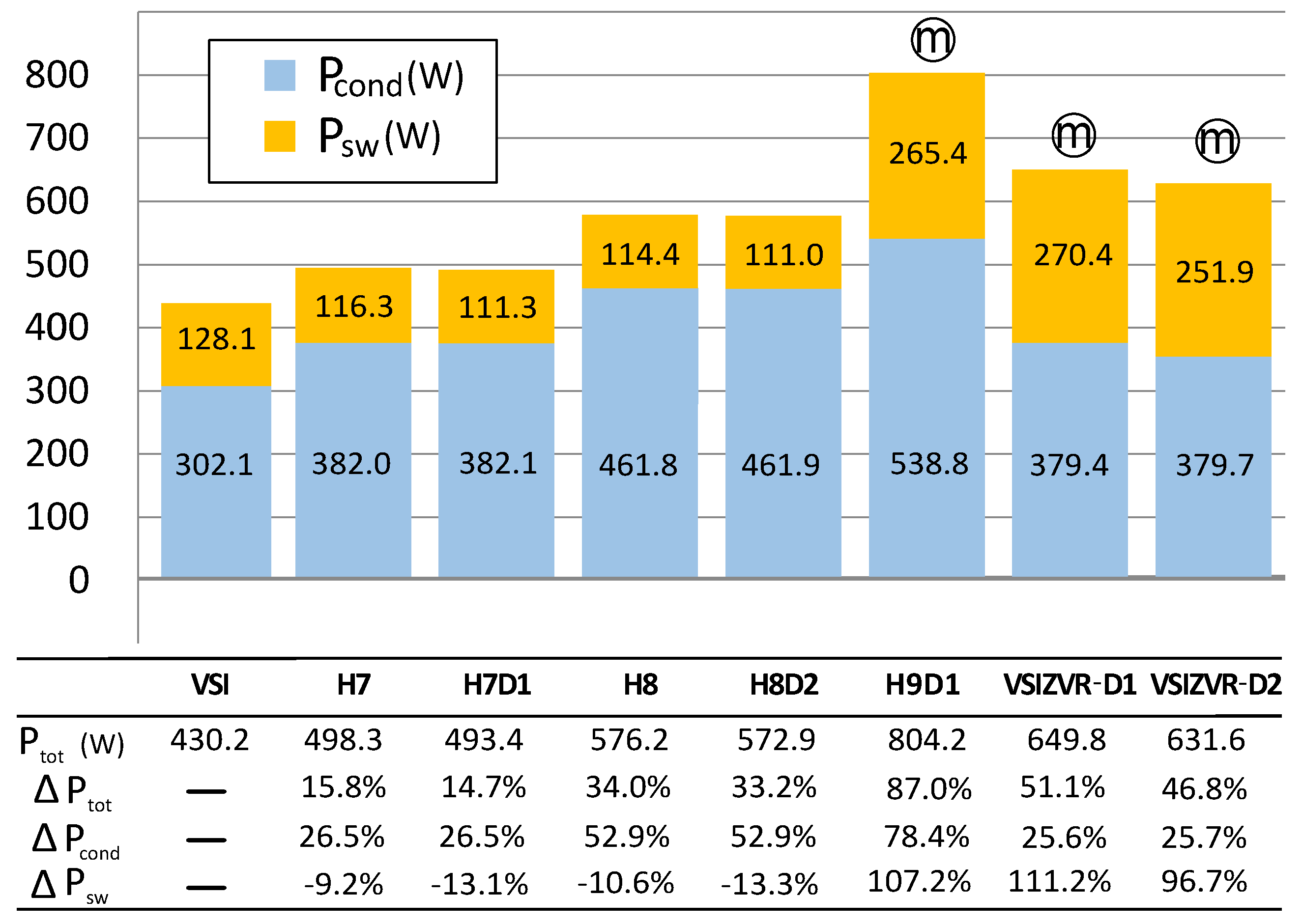
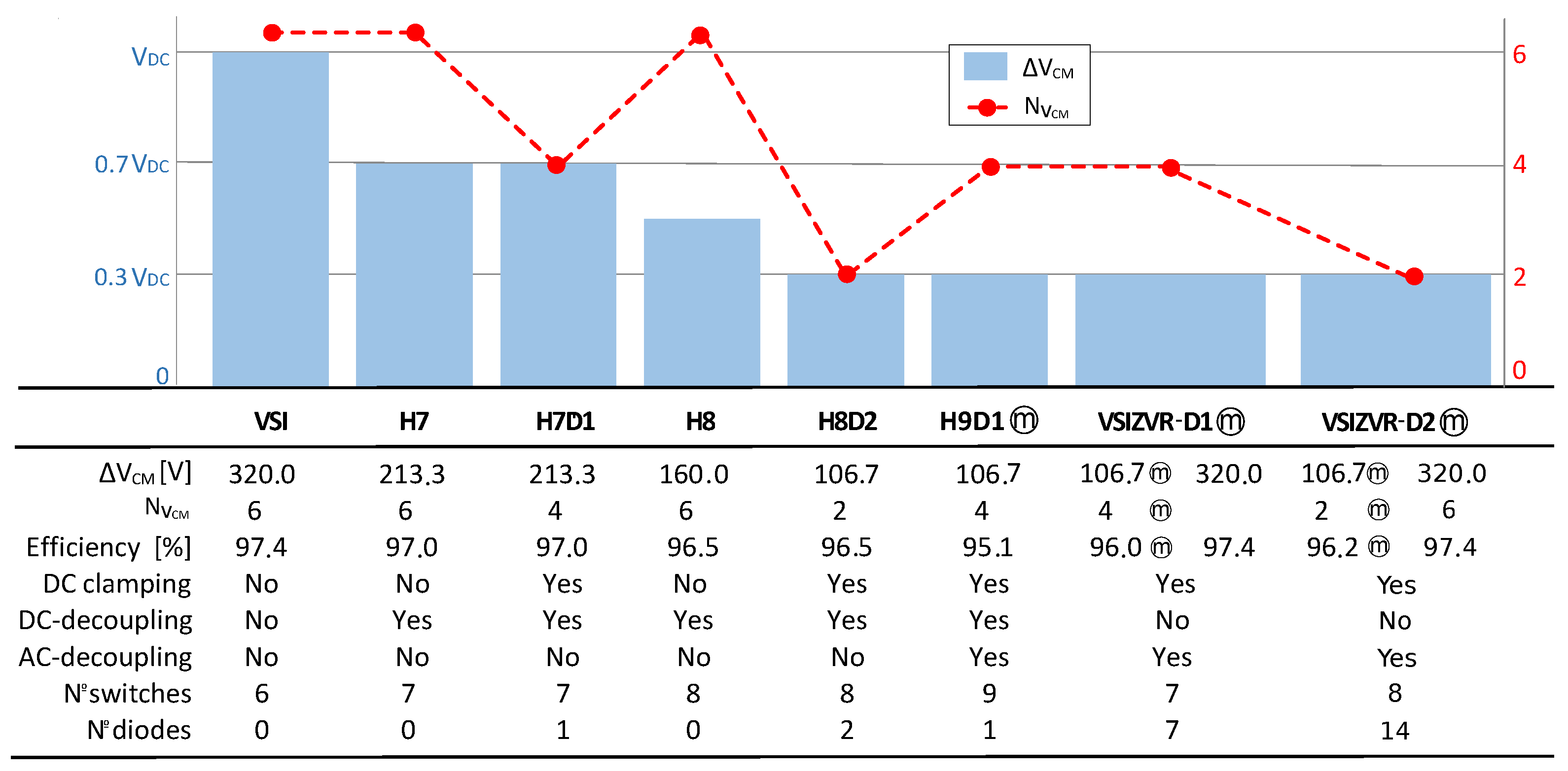
4.1. Comparison of the Studied Topologies
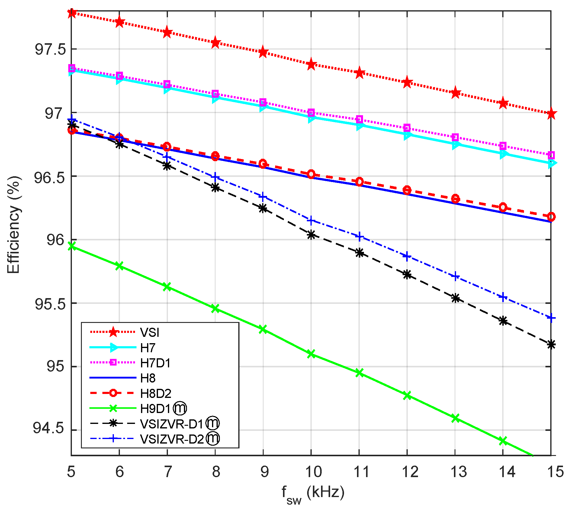
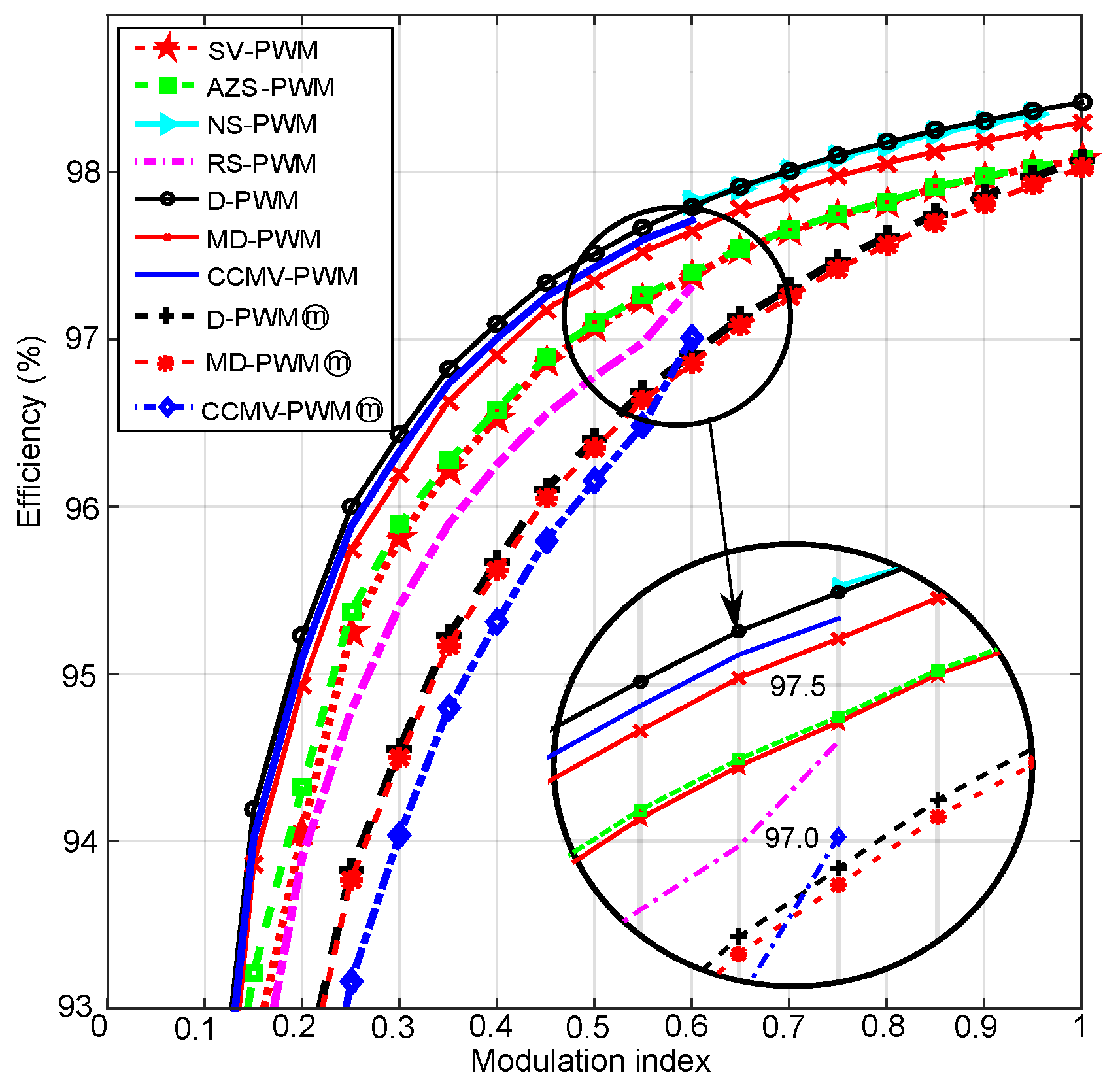
operation mode) and the H8D2. Both improved the and up to 66.6% when compared to the traditional VSI. Followed by these were the H9D1 and VSIZVR-D1 topologies, improving up to 66.6%, but only improving up to 33.3% due to the greater number of vector transitions. Without using the clamping method, the H8 topology improved up to 50% (but with the same as the VSI). Finally, the H7 and H7D1 topologies improved up to 33.3% and up to 33.3%. is represented for the AC-decoupling topologies, the efficiency would correspond to the VSI curve in the case of VSIZVR-D1 and VSIZVR-D2 when using traditional modulations without modifications). On the other hand, the distribution between conduction and switching losses varies according to the topology. For example, the DC-decoupling topologies increased the conduction losses, but reduced the switching losses (Figure 11).4.2. Analysis of the Influence of the Modulation Technique on the VSIZVR-D2 Topology
) and the rectifiers were activated, the CMV was completely eliminated.), the efficiency was also reduced. Otherwise, without using them, the efficiencies were higher than in the VSI with SV-PWM.5. VSIZVR-D2 Topology Performance during Realistic Driving Conditions
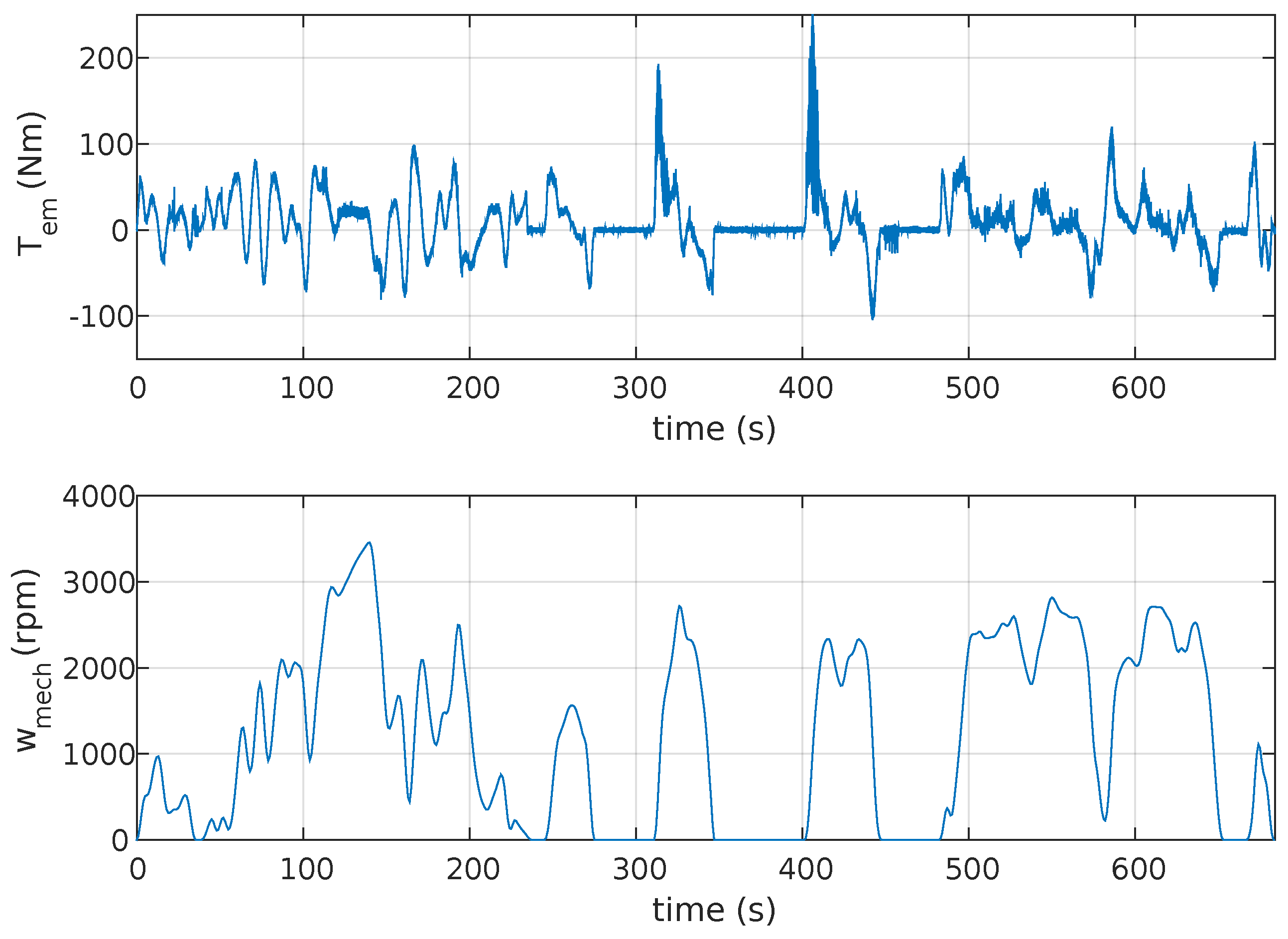
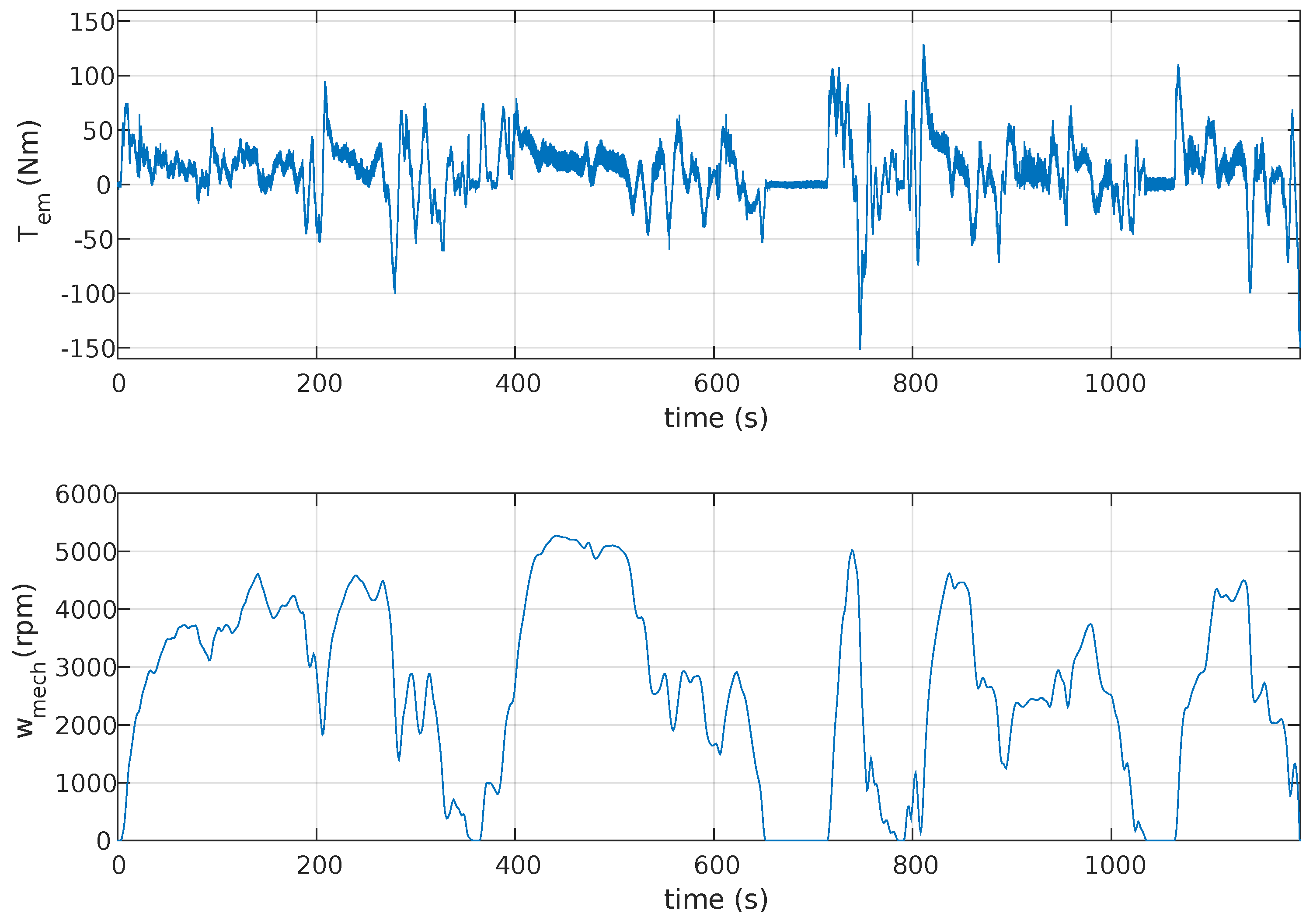
(when M < 0.57). The other one, named Hybrid 2, combined the D-PWM (when M > 0.57) and the CCMV-PWM (when M < 0.57).5.1. Results of the VSIZVR-D2 Topology under the Fleet-BEV-Urban-Cycle
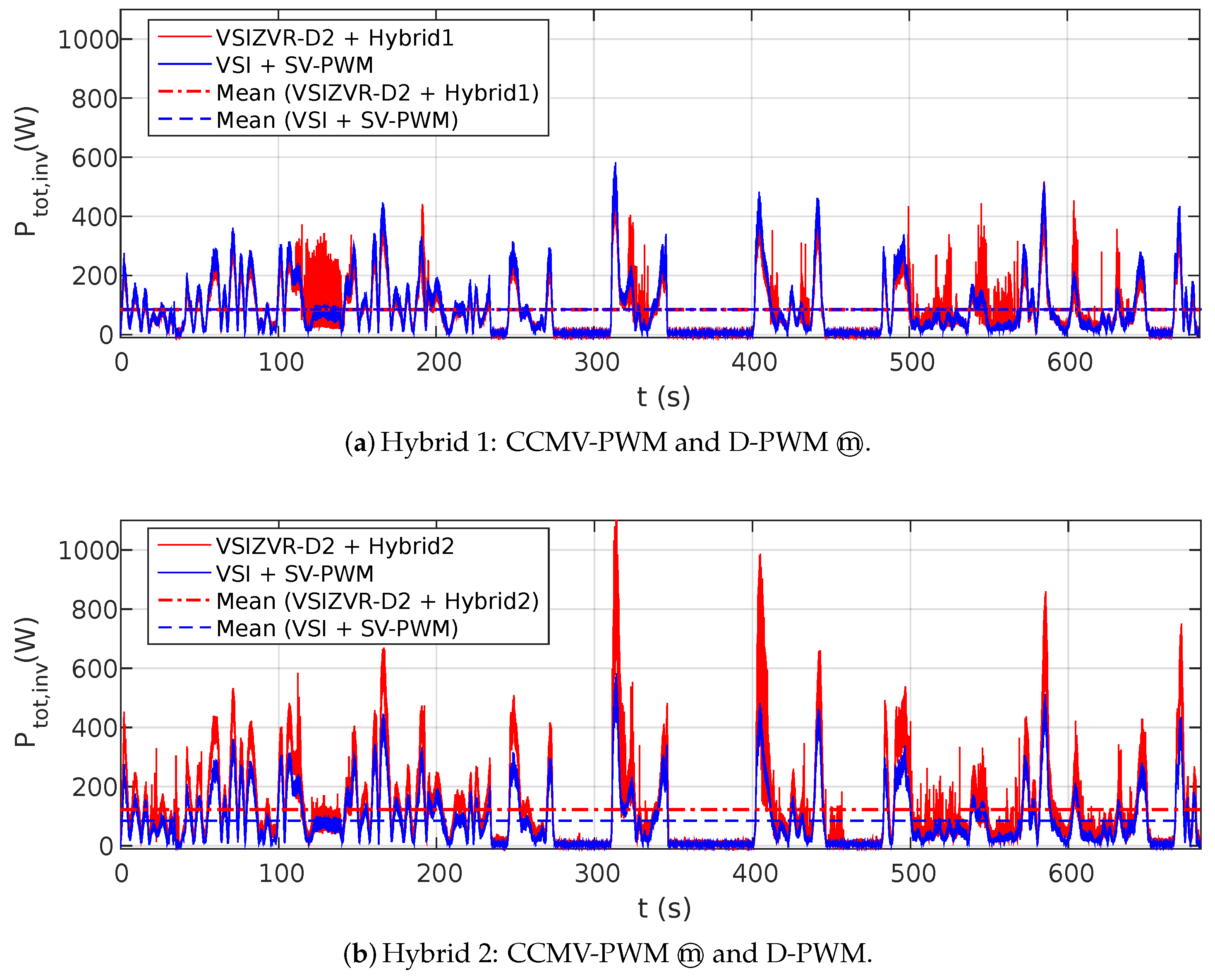
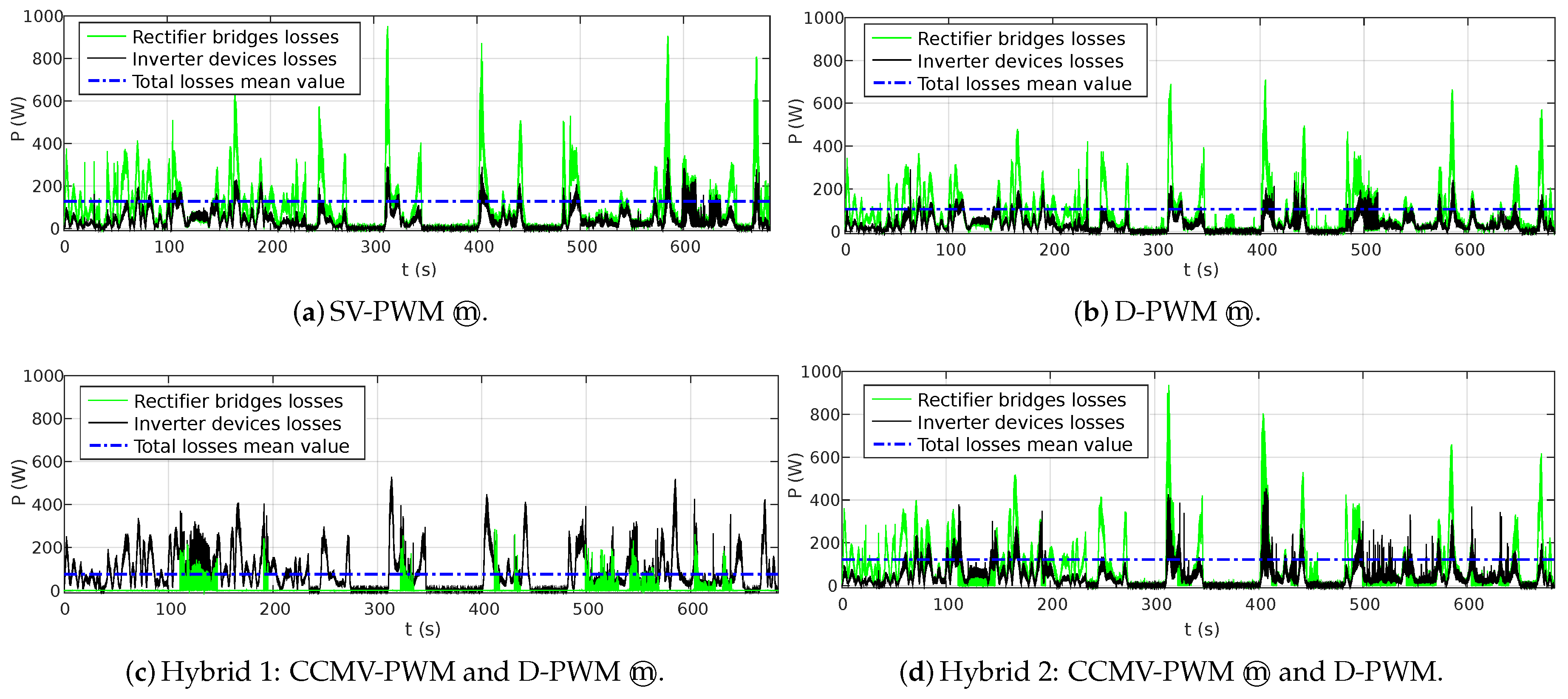
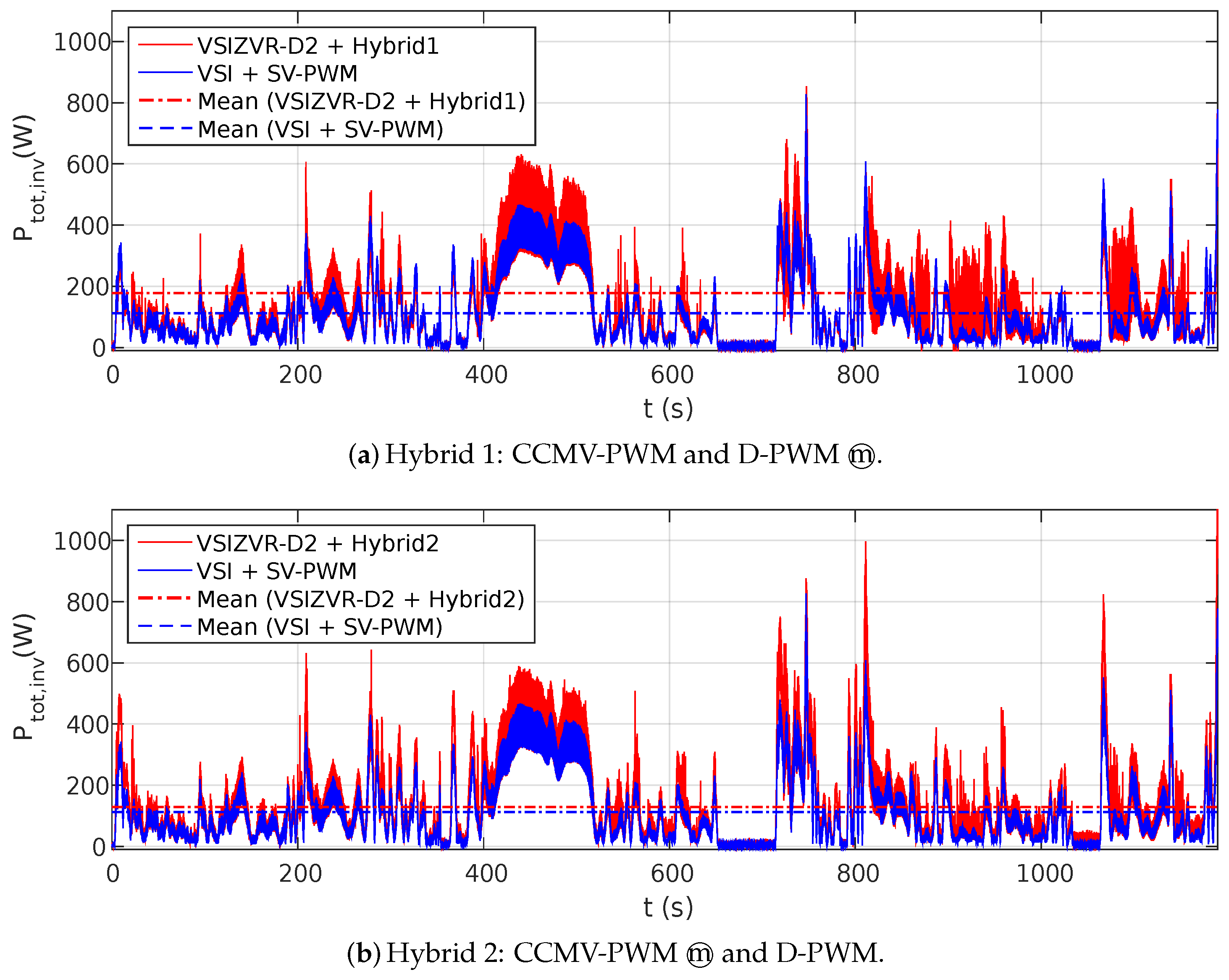
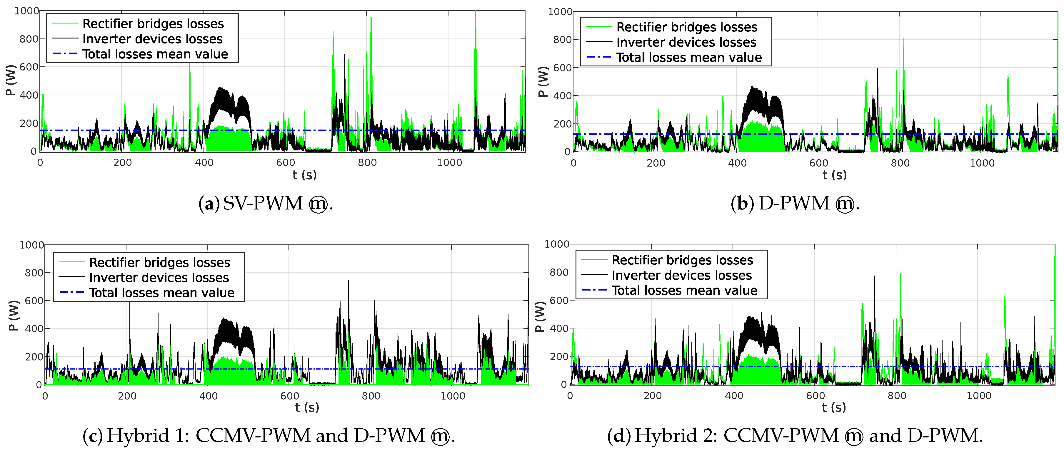
modified techniques had a lower converter efficiency, but were able to reduce CMV to a greater extent. In addition, when using hybrid modulations, a similar efficiency to the VSI topology with SV-PWM could be achieved, at the cost of losing some CMV reduction capability. In this sense, Figure 18 compares the VSI topology (using the SV-PWM modulation technique) and the VSIZVR-D2 using the hybrid modulations Hybrid 1 and Hybrid 2. It can be seen that the average values of the power losses were close in both curves. In addition, Figure 19 shows (for the studied modulation techniques) how the power converter losses were distributed between the traditional inverter devices and the rectifier bridges in the new VSIZVR-D2 inverter topology.5.2. Results of the VSIZVR-D2 Topology under the Fleet-BEV-Rural-Cycle
6. Conclusions
Author Contributions
Funding
Conflicts of Interest
Abbreviations
| AC | Alternating current |
| AZS-PWM | Active zero-state pulse width modulation |
| CCMV-PWM | Constant common mode voltage pulse width modulation |
| CMV | Common mode voltage |
| DC | Direct current |
| D-PWM | Discontinuous pulse width modulation |
| EDM | Electric discharge machining |
| EMI | Electromagnetic interferences |
| EV | Electric vehicle |
| Fleet-BEV | Fleet battery electric vehicle |
| FOC | Field-oriented control |
| HBZVR | H-Bridge zero-voltage rectifier |
| HERIC | High efficient and reliable inverter concept |
| IGBT | Insulated gate bipolar transistor |
| MD-PWM | Modified discontinuous pulse width modulation |
| NS-PWM | Near-state pulse width modulation |
| PWM | Pulse width modulation |
| RCMV-PWM | Reduced common mode voltage pulse width modulation |
| RS-PWM | Remote-state pulse width modulation |
| RT | Real time |
| SM-PMSM | Surface mounted permanent magnet synchronous machine |
| SV-PWM | Space vector pulse width modulation |
| THD | Total harmonic distortion |
| VSI | Voltage source inverter |
| VSIZVR | Voltage source inverter zero-voltage rectifier |
| WBG | Wide bandgap |
Appendix A. Description of the Power Loss and Thermal Model

| Parameter | Symbol | Value | Units |
|---|---|---|---|
| Nominal current per switch | 120 | A | |
| Maximum blocking voltage | 600 | V | |
| Typical collector-emitter voltage | 1.7 | V | |
| Typical turn-on switching loss | 8.2 | mJ | |
| Typical turn-off switching loss | 2.9 | mJ | |
| Typical diode reverse recovery | 2.4 | mJ | |
| Allowable junction temperature | −55 to +175 | C |

| Parameter | Symbol | Value | Units |
|---|---|---|---|
| 0.0564 | |||
| IGBT thermal resistances | 0.0888 | C/W | |
| 0.0547 | |||
| 0.0045 | |||
| IGBT thermal capacitances | 0.0355 | Ws/C | |
| 0.2723 | |||
| 0.0060 | |||
| IGBT thermal resistances | 0.1404 | C/W | |
| 0.1912 | |||
| 0.1016 | |||
| 0.0027 | |||
| Diode thermal capacitances | 0.0028 | Ws/C | |
| 0.0214 | |||
| 0.2092 |
References
- Kumar, M.S.; Revankar, S.T. Development scheme and key technology of an electric vehicle: An overview. Renew. Sustain. Energy Rev. 2017, 70, 1266–1285. [Google Scholar] [CrossRef]
- International Energy Agency. Energy Technology Perspectives; Technical Report; International Energy Agency: Paris, France, 2017. [Google Scholar]
- Riba, J.R.; López-Torres, C.; Romeral, L.; Garcia, A. Rare-earth-free propulsion motors for electric vehicles: A technology review. Renew. Sustain. Energy Rev. 2016, 57, 367–379. [Google Scholar] [CrossRef]
- Horizon 2020. The EU Framework Programme for Research and Innovation. Technical Report. Available online: https://ec.europa.eu/programmes/horizon2020 (accessed on 29 August 2019).
- United States Council for Automotive Rresearch LLC. Technical Report. Available online: http://www.uscar.org/guest/index.php (accessed on 29 August 2019).
- Espina, J.; Balcells, J.; Arias, A.; Ortega, C. Common mode EMI model for a direct matrix converter. IEEE Trans. Ind. Electron. 2011, 58, 5049–5056. [Google Scholar] [CrossRef]
- Chen, K.; Hsieh, M. Generalized Minimum Common-Mode Voltage PWM for Two-Level Multiphase VSIs Considering Reference Order. IEEE Trans. Power Electron. 2017, 32, 6493–6509. [Google Scholar] [CrossRef]
- Jeschke, S.; Tsiapenko, S.; Hirsch, H. Investigations on the shaft currents of an electric vehicle traction system in dynamic operation. In Proceedings of the IEEE International Symposium on Electromagnetic Compatibility (EMC), Dresden, Germany, 16–22 August 2015; pp. 696–701. [Google Scholar]
- Asefi, M.; Nazarzadeh, J. Survey on high-frequency models of PWM electric drives for shaft voltage and bearing current analysis. IET Electr. Syst. Transp. 2017, 7, 179–189. [Google Scholar] [CrossRef]
- Hadden, T.; Jiang, J.W.; Bilgin, B.; Yang, Y.; Sathyan, A.; Dadkhah, H.; Emadi, A. A Review of Shaft Voltages and Bearing Currents in EV and HEV Motors. In Proceedings of the Conference of the IEEE Industrial Electronics Society (IECON), Florence, Italy, 23–26 October 2016; pp. 1578–1583. [Google Scholar]
- Euerle, K.; Iyer, K.; Severson, E.; Baranwal, R.; Tewari, S.; Mohan, N. A compact active filter to eliminate common-mode voltage in a SiC-based motor drive. In Proceedings of the IEEE Energy Conversion Congress and Exposition (ECCE), Milwaukee, WI, USA, 18–22 September 2016; pp. 1–8. [Google Scholar]
- Mütze, A. Thousands of hits: On inverter-induced bearing currents, related work, and the literature. Elektrotechnik Und Informationstechnik 2011, 128, 382–388. [Google Scholar] [CrossRef]
- Muetze, A.; Binder, A. Don’t lose your bearings. IEEE Ind. Appl. Mag. 2006, 12, 22–31. [Google Scholar] [CrossRef]
- Schiferl, R.F.; Melfi, M.J. Bearing current remediation options. IEEE Ind. Appl. Mag. 2004, 10, 40–50. [Google Scholar] [CrossRef]
- ABB Drives. Technical Guide No. 5: Bearing Currents in Modern AC Drive Systems; Technical Report. ABB Drives, 2011. Available online: https://docplayer.net/30472048-Abb-drives-technical-guide-no-5-bearing-currents-in-modern-ac-drive-systems.html (accessed on 29 August 2019).
- Eaton Corporation. Bearing Currents Application Note AP040061E; Technical Report; Eaton Corporation: Dublin, Ireland, 2014. [Google Scholar]
- Willwerth, A. To Be Considered “True Inverter-Duty”, Motors Need Bearing Protection; Technical Report; Electro Static Technology (AEGIS): Mechanic Falls, ME, USA, 2016. [Google Scholar]
- Reimers, J.; Dorn-Bomba, L.; Mak, C.; Emadi, A. Automotive traction inverters: Current status and future trends. IEEE Trans. Veh. Technol. 2019, 68, 3337–3350. [Google Scholar] [CrossRef]
- Oustad, D.; Ameziani, M.; Lhotellier, D.; Lefebvre, S.; Petit, M. Estimation of the Losses in Si and SiC Power Modules for Automotive Applications. In Proceedings of the International Exhibition and Conference for Power Electronics, Intelligent Motion, Renewable Energy and Energy Management (PCIM), Shanghai, China, 27–29 June 2017; pp. 1–8. [Google Scholar]
- Chen, S.; Lipo, T.A. Bearing currents and shaft voltages of an induction motor under hard- and soft-switching inverter excitation. IEEE Trans. Ind. Appl. 1998, 34, 1042–1048. [Google Scholar] [CrossRef]
- Concari, L.; Barater, D.; Buticchi, G.; Concari, C.; Liserre, M. H8 Inverter for Common-Mode Voltage Reduction in Electric Drives. IEEE Trans. Ind. Appl. 2016, 52, 4010–4019. [Google Scholar] [CrossRef]
- Gao, H.; Wu, B.; Xu, D.; Pande, M.; Aguilera, R. Common-Mode-Voltage-Reduced Model-Predictive Control Scheme for Current-Source-Converter-Fed Induction Motor Drives. IEEE Trans. Power Electron. 2017, 32, 4891–4904. [Google Scholar] [CrossRef]
- Han, Y.; Lu, H.; Li, Y.; Chai, J. Analysis and Suppression of Shaft Voltage in SiC-based Inverter for Electric Vehicle Applications. IEEE Trans. Power Electron. 2018. [Google Scholar] [CrossRef]
- Hava, A.M.; Ün, E. Performance Analysis of Reduced Common-Mode Voltage PWM Methods and Comparison With Standard PWM Methods for Three-Phase Voltage-Source Inverters. IEEE Trans. Power Electron. 2009, 24, 241–252. [Google Scholar] [CrossRef]
- Ronanki, D.; Sang, P.H.; Sood, V.; Williamson, S.S. Comparative assessment of three-phase transformerless grid-connected solar inverters. In Proceedings of the IEEE International Conference on Industrial Technology (ICIT), Toronto, ON, Canada, 22–25 March 2017; pp. 66–71. [Google Scholar]
- Suan, F.T.K.; Rahim, N.A.; Ping, H.W. An improved three-phase transformerless photovoltaic inverter with reduced leakage currents. In Proceedings of the IET International Conference on Clean Energy and Technology (CEAT), Kuching, Malaysia, 24–26 November 2014; pp. 1–4. [Google Scholar]
- Nguyen, N.; Nguyen, T.; Lee, H. A reduced siwtching loss PWM strategy to eliminate common-mode voltage in multilevel inverters. IEEE Trans. Power Electron. 2015, 30, 5425–5438. [Google Scholar] [CrossRef]
- Liu, X.; Wang, D.; Peng, Z. An improved finite control-set model predictive control for nested neutral point-clamped converters under both balanced and unbalanced grid conditions. Int. J. Electr. Power Energy Syst. 2019, 104, 910–923. [Google Scholar] [CrossRef]
- Panda, A.K.; Suresh, Y. Research on cascade multilevel inverter with single DC source by using three-phase transformers. Int. J. Electr. Power Energy Syst. 2012, 40, 9–20. [Google Scholar] [CrossRef]
- Jung, C. Power up with 800-V systems. IEEE Electrif. Mag. 2017, 5, 53–58. [Google Scholar] [CrossRef]
- Gupta, K.K.; Jain, S. A multilevel Voltage Source Inverter (VSI) to maximize the number of levels in output waveform. Int. J. Electr. Power Energy Syst. 2013, 44, 25–36. [Google Scholar] [CrossRef]
- Syed, A.; Kalyani, S. Evaluation of single phase transformerless photovoltaic inverters. Electr. Electron. Eng. Int. J. 2015, 4, 25–39. [Google Scholar] [CrossRef]
- Patrao, I.; Figueres, E.; González-Espín, F.; Garcerá, G. Transformerless topologies for grid-connected single-phase photovoltaic inverters. Renew. Sustain. Energy Rev. 2011, 15, 3423–3431. [Google Scholar] [CrossRef]
- Kerekes, T.; Teodorescu, R.; Rodriguez, P.; Vazquez, G.; Aldabas, E. A New High-Efficiency Single-Phase Transformerless PV Inverter Topology. IEEE Trans. Ind. Electron. 2011, 58, 184–191. [Google Scholar] [CrossRef]
- Kouro, S.; Leon, J.I.; Vinnikov, D.; Franquelo, L.G. Grid-Connected Photovoltaic Systems: An Overview of Recent Research and Emerging PV Converter Technology. IEEE Ind. Electron. Mag. 2015, 9, 47–61. [Google Scholar] [CrossRef]
- Freddy, T.K.S.; Rahim, N.A.; Hew, W.P.; Che, H.S. Comparison and Analysis of Single-Phase Transformerless Grid-Connected PV Inverters. IEEE Trans. Power Electron. 2014, 29, 5358–5369. [Google Scholar] [CrossRef]
- Freddy, T.K.S.; Rahim, N.A.; Hew, W.P.; Che, H.S. Modulation Techniques to Reduce Leakage Current in Three-Phase Transformerless H7 Photovoltaic Inverter. IEEE Trans. Ind. Electron. 2015, 62, 322–331. [Google Scholar] [CrossRef]
- Sarlioglu, B.; Morris, C.; Han, D.; Li, S. A review of technological improvements for electric machines, power electronics, and batteries for electric and hybrid vehicles. IEEE Ind. Appl. Mag. 2017, 23, 14–25. [Google Scholar] [CrossRef]
- Bharatiraja, C.; Jeevananthan, S.; Munda, J.; Latha, R. Improved SVPWM vector selection approaches in OVM region to reduce common-mode voltage for three-level neutral point clamped inverter. Int. J. Electr. Power Energy Syst. 2016, 79, 285–297. [Google Scholar] [CrossRef]
- Dabour, S.M.; Abdel-Khalik, A.S.; Ahmed, S.; Massoud, A.M.; Allam, S. Common-mode voltage reduction for space vector modulated three- to five-phase indirect matrix converter. Int. J. Electr. Power Energy Syst. 2018, 95, 266–274. [Google Scholar] [CrossRef]
- Rahimi, R.; Farhangi, S.; Farhangi, B.; Moradi, G.R.; Afshari, E.; Blaabjerg, F. H8 Inverter to Reduce Leakage Current in Transformerless Three-Phase Grid-Connected Photovoltaic systems. IEEE J. Emerg. Sel. Top. Power Electron. 2018, 6, 910–918. [Google Scholar] [CrossRef]
- Guo, X.; Xu, D.; Wu, B. Three-phase DC-bypass topologies with reduced leakage current for transformerless PV systems. In Proceedings of the IEEE Energy Conversion Congress and Exposition (ECCE), Montreal, QC, Canada, 20–24 September 2015; pp. 43–46. [Google Scholar]
- Concari, L.; Barater, D.; Toscani, A.; Concari, C.; Franceschini, G.; Buticchi, G.; Liserre, M.; Zhang, H. Assessment of Efficiency and Reliability of Wide Band-Gap Based H8 Inverter in Electric Vehicle Applications. Energies 2019, 12, 1922. [Google Scholar] [CrossRef]
- Guo, X.; Xu, D.; Wu, B. Three-phase seven-switch inverter with common mode voltage reduction for transformerless photovoltaic system. In Proceedings of the Conference of the IEEE Industrial Electronics Society (IECON), Yokohama, Japan, 9–12 November 2015; pp. 2279–2284. [Google Scholar]
- Vazquez, G.; Kerekes, T.; Rocabert, J.; Rodríguez, P.; Teodorescu, R.; Aguilar, D. A photovoltaic three-phase topology to reduce Common Mode Voltage. In Proceedings of the IEEE International Symposium on Industrial Electronics (ISIE), Bari, Italy, 4–7 July 2010; pp. 2885–2890. [Google Scholar]
- Matallana, A.; Ibarra, E.; López, I.; Andreu, J.; Garate, J.; Jorda, X.; Rebollo, J. Power module electronics in HEV/EV applications: New trends in wide-bandgap semiconductor technologies and design aspects. Renew. Sustain. Energy Rev. 2019, 113, 1–33. [Google Scholar] [CrossRef]
- Robles, E.; Fernandez, M.; Ibarra, E.; Andreu, J.; Kortabarria, I. Modelado y simulacion de perdidas en convertidores de potencia aplicados al vehiculo electrico. In Proceedings of the Seminario Anual de Automática, Electrónica Industrial e Instrumentación (SAAEI), Barcelona, Spain, 4–6 July 2018. [Google Scholar]
- Shue, S.; Pan, C. Voltage-constraint-tracking-based field-weakening control for IPM synchronous motor drives. IEEE Trans. Ind. Electron. 2008, 55, 340–347. [Google Scholar] [CrossRef]
- Li, Q.; Chen, W.; Li, Y.; Liu, S.; Huang, J. Energy management strategy for fuel cell/battery/ultracapacitor hybrid vehicle based on fuzzy logic. Int. J. Electr. Power Energy Syst. 2012, 43, 514–525. [Google Scholar] [CrossRef]
- Trancho, E.; Ibarra, E.; Arias, A.; Kortabarria, I.; Prieto, P.; de Alegria, I.M.; Andreu, J.; Lopez, I. Sensorless control strategy for light-duty EVs and efficiency loss evaluation of high frequency injection under standardized urban driving cycles. Appl. Energy 2018, 224, 647–658. [Google Scholar] [CrossRef]
- Pfriem, M.; Gauterin, F. Development of real-world Driving Cycles for Battery Electric Vehicles. In Proceedings of the International Battery, Hybrid and Fuel Cell Electric Vehicle Symposium (EVS29), Montreal, QC, Canada, 19–22 June 2016. [Google Scholar]
- Sadigh, A.K.; Dargahi, V.; Corzine, K. Analytical determination of conduction power loss and investigation of switching power loss for modified flying capacitor multicell converters. IET Power Electron. 2016, 9, 175–187. [Google Scholar] [CrossRef]


 ; (b) D-PWM ; (c) Hybrid 1; (d) Hybrid 2.
; (b) D-PWM ; (c) Hybrid 1; (d) Hybrid 2.
; (b) D-PWM ; (c) Hybrid 1; (d) Hybrid 2.

 ; (b) D-PWM ; (c) Hybrid 1; (d) Hybrid 2.
; (b) D-PWM ; (c) Hybrid 1; (d) Hybrid 2.
; (b) D-PWM ; (c) Hybrid 1; (d) Hybrid 2.
| Topology | ||||||
|---|---|---|---|---|---|---|
| Item | Full-Bridge (unipolar modulation) | Full-Bridge (bipolar modulation) | H5 | H6D2 | HBZVR-D | HERIC |
| Switches | 4 | 4 | 5 | 6 | 5 | 6 |
| Capacitors | 1 | 1 | 1 | 2 | 2 | 1 |
| Diodes | 0 | 0 | 0 | 2 | 6 | 2 |
| Efficiency | ✓ | ✗ | ✓ | ✓ | ✓ | ✓✓ |
| CMV | ✗ | ✓✓ | ✗ | ✓✓ | ✓✓ | ✓ |
| Leakage current | ✗✗ | ✓ | ✓✓ | ✓✓ | ✓✓ | ✓✓ |
| Advantages | High efficiency | Constant CMV, low leakage current | Low current ripple | Constant CMV, low leakage current | Very low leakage current, high efficiency | Without losses during freewheeling, high efficiency |
| Disadvantages | High leakage current | Very high current ripple, impaired signal quality, 2 voltage levels, low efficiency | Losses during freewheeling, high switching losses, variable CMV | High conduction losses | Bipolar output voltage due to dead time between driving and freewheeling mode | Injection of reactive power to the grid, floating CMV |
| References | [32,33,34] | [32,33] | [32,33,35,36] | [32,35,36] | [32,34,36] | [32,33,34,35] |
| PWM Method | References | Sequence (Depending on the Plane Sector) | |||||
|---|---|---|---|---|---|---|---|
| SV-PWM | [21] | 0127210 | 0327230 | 0347430 | 0547450 | 0567650 | 0167610 |
| AZS-PWM | [25,37] | 6123216 | 4321234 | 2345432 | 6543456 | 4561654 | 2165612 |
| RS-PWM | [24,25] | 31513 | 31513 | 31513 | 31513 | 31513 | 31513 |
| NS-PWM | [24,25,37] | 21612 | 32123 | 43234 | 54345 | 65456 | 16561 |
| CCMV-PWM | [21] | 10301 | 30103 | 30503 | 50305 | 50105 | 10501 |
| D-PWM | [25,26,37] | 72127 | 23032 | 74347 | 45054 | 76567 | 61016 |
| MD-PWM | [25,26,37] | 72127 | 23732 | 74347 | 45754 | 76567 | 61716 |
| Voltage | Switching | CMV Depending on Each Topology | |||||||
|---|---|---|---|---|---|---|---|---|---|
| Vectors | States | VSI | H7 | H7D1 | H8 | H8D2 | H9D1  | VSIZVR-D1 | VSIZVR-D2 |
| 000 | |||||||||
| 100 | |||||||||
| 110 | |||||||||
| 010 | |||||||||
| 011 | |||||||||
| 001 | |||||||||
| 101 | |||||||||
| 111 | |||||||||
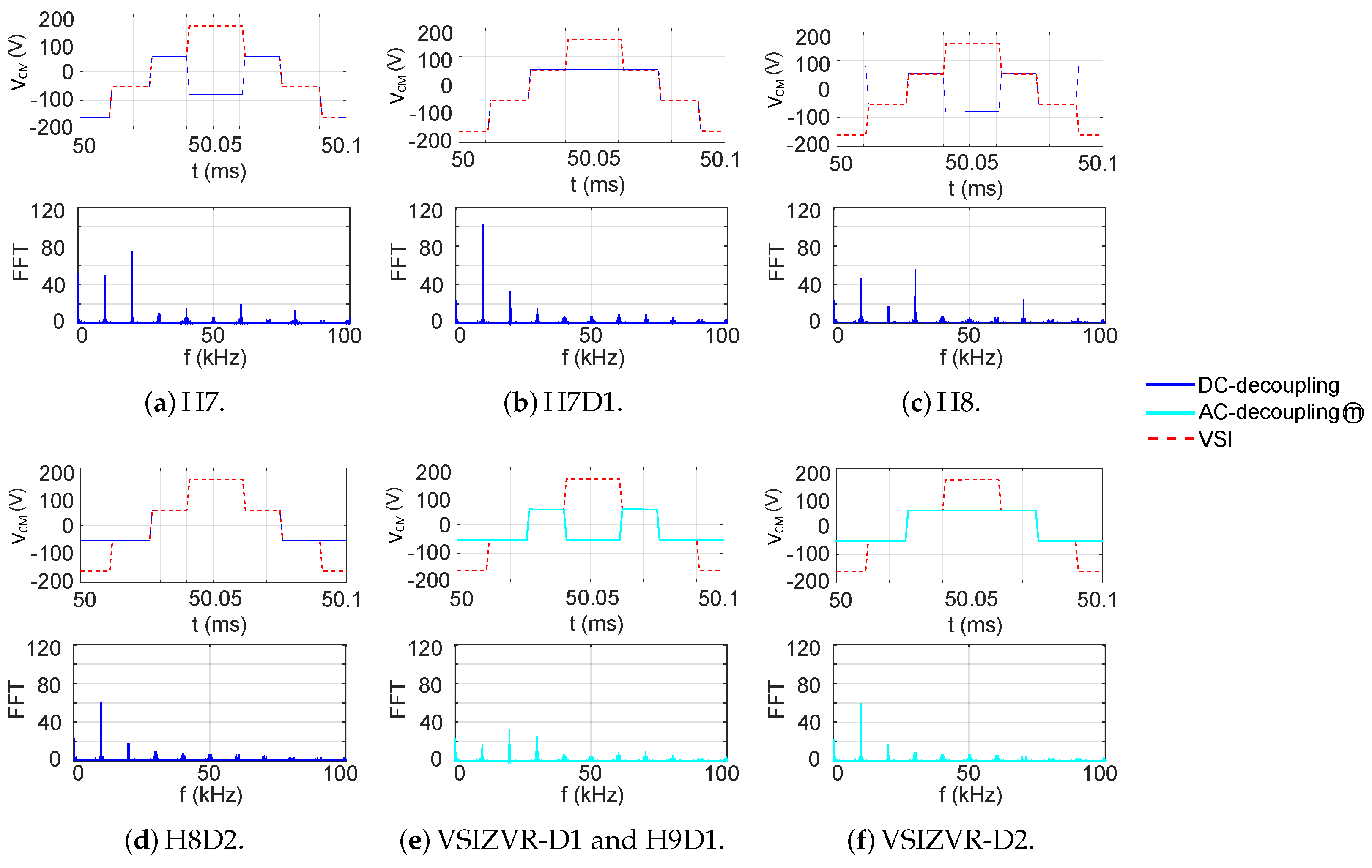
| SV-PWM CMV waveforms |  |  |  |  |  |  |  |  | |
Operation Mode 2 of the AC-decoupling topologies.| Devices | Losses | ||||
|---|---|---|---|---|---|
| Topology | (W) | (W) | (W) | (W) | |
| VSI | – | 37.2 | 13.1 | 19.2 | 2.6 |
| – | - | - | - | - | |
| – | - | - | - | - | |
| – | - | - | - | - | |
| VSIZVR-D2 | – | 26.8 | 1.1 | 16.9 | 0.7 |
| – | 34.5 | - | 61.1 | - | |
| – | - | 11.9 | - | 2.1 | |
| – | - | 11.9 | - | 2.1 | |
| Modulation | Voltage Linearity | Phase Current | Current THD | CMV Amplitude | Num. CMV Variations | CMV Levels | DC-link Current Ripple | Output Current Ripple | Efficiency | ||||
|---|---|---|---|---|---|---|---|---|---|---|---|---|---|
| [] | (%) | dev. (%) | dev. (%) | [] | dev. (%) | [] | dev. (%) | (%) | |||||
| SV-PWM | 0–1 | 104.5 | 1.1 | 320.0 | - | 6 | - | 4 | 32.4 | - | 2.2 | - | 97.4 |
| AZS-PWM | 0–1 | 104.5 | 2.7 | 106.7 | −66.7 | 6 | 0 | 2 | 34.3 | 5.6 | 3.3 | 49.5 | 97.4 |
| NS-PWM | 0.67–1 | 107.4 | 2.8 | 106.7 | −66.7 | 2 | −66.7 | 2 | 19.6 | −39.5 | 2.2 | 0.0 | 97.8 |
| RS-PWM | 0–0.57 | 104.6 | 2.5 | 0.0 | −100.0 | 0 | −100.0 | 1 | 32.5 | 0.3 | 3.6 | 60.4 | 97.3 |
| D-PWM | 0–1 | 105.1 | 1.6 | 320.0 | 0 | 4 | −33.3 | 4 | 22.9 | −29.5 | 2.5 | 12.2 | 97.8 |
| MD-PWM | 0–1 | 105.1 | 1.6 | 213.3 | −33.3 | 4 | −33.3 | 3 | 22.9 | −29.5 | 2.5 | 12.2 | 97.7 |
| CCMV-PWM | 0–0.57 | 104.9 | 2.5 | 213.3 | −33.3 | 3 | −50.0 | 2 | 23.1 | −28.8 | 1.2 | −48.2 | 97.7 |
| D-PWM | 0–1 | 105.1 | 1.6 | 106.7 | −66.7 | 2 | −66.7 | 2 | 22.9 | −29.5 | 2.5 | 12.2 | 96.9 |
| MD-PWM | 0–1 | 105.1 | 1.6 | 106.7 | −66.7 | 3 | −50.0 | 2 | 22.9 | −29.5 | 2.5 | 12.2 | 96.9 |
| CCMV-PWM | 0–0.57 | 104.9 | 2.5 | 0.0 | −100.0 | 0 | −100.0 | 1 | 23.1 | −28.8 | 1.1 | −48.7 | 97.0 |
| Modulation Technique | CCMV-PWM Utilization (%) | D-PWM Utilization (%) | SV-PWM Utilization (%) | Efficiency (%) | Reduction (%) | Reduction (%) | Average Power Dissipated (W) | Dev. Average Power Dissipated (%) |
|---|---|---|---|---|---|---|---|---|
| SV-PWM | 0 | 0 | 100 | 97.3 | - | - | 84.8 | - |
| SV-PWM | 0 | 0 | 100 | 96.0 | −66.7 | −66.7 | 129.0 | 52.1 |
| D-PWM | 0 | 100 | 0 | 97.7 | −33.3 | 0 | 71.9 | −15.2 |
| D-PWM | 0 | 100 | 0 | 96.6 | −66.7 | −66.7 | 106.9 | 26.1 |
| Hybrid 1 | 90.2 | 9.8 | 0 | 97.3 | −51.6 | −36.6 | 84.3 | −0.6 |
| Hybrid 2 | 90.5 | 9.5 | 0 | 96.1 | −93.7 | −90.5 | 122.5 | 44.5 |
| Modulation Technique | CCMV-PWM Utilization (%) | D-PWM Utilization (%) | SV-PWM Utilization (%) | Efficiency (%) | Reduction (%) | Reduction (%) | Average Power Dissipated (W) | Dev. Average Power Dissipated (%) |
|---|---|---|---|---|---|---|---|---|
| SV-PWM | 0 | 0 | 100 | 98.3 | - | - | 112.6 | - |
| SV-PWM | 0 | 0 | 100 | 97.7 | −66.7 | −66.7 | 148.7 | 32.1 |
| D-PWM | 0 | 100 | 0 | 98.4 | −33.3 | 0 | 101.8 | −9.6 |
| D-PWM | 0 | 100 | 0 | 97.9 | −66.7 | −66.7 | 131.2 | 16.5 |
| Hybrid 1 | 51.3 | 48.7 | 0 | 95.5 | −58.1 | −49.6 | 177.6 | 57.7 |
| Hybrid 2 | 51.4 | 48.6 | 0 | 98.0 | −67.6 | −51.4 | 129.3 | 14.8 |
© 2019 by the authors. Licensee MDPI, Basel, Switzerland. This article is an open access article distributed under the terms and conditions of the Creative Commons Attribution (CC BY) license (http://creativecommons.org/licenses/by/4.0/).
Share and Cite
Robles, E.; Fernandez, M.; Ibarra, E.; Andreu, J.; Kortabarria, I. Mitigation of Common Mode Voltage Issues in Electric Vehicle Drive Systems by Means of an Alternative AC-Decoupling Power Converter Topology. Energies 2019, 12, 3349. https://doi.org/10.3390/en12173349
Robles E, Fernandez M, Ibarra E, Andreu J, Kortabarria I. Mitigation of Common Mode Voltage Issues in Electric Vehicle Drive Systems by Means of an Alternative AC-Decoupling Power Converter Topology. Energies. 2019; 12(17):3349. https://doi.org/10.3390/en12173349
Chicago/Turabian StyleRobles, Endika, Markel Fernandez, Edorta Ibarra, Jon Andreu, and Iñigo Kortabarria. 2019. "Mitigation of Common Mode Voltage Issues in Electric Vehicle Drive Systems by Means of an Alternative AC-Decoupling Power Converter Topology" Energies 12, no. 17: 3349. https://doi.org/10.3390/en12173349
APA StyleRobles, E., Fernandez, M., Ibarra, E., Andreu, J., & Kortabarria, I. (2019). Mitigation of Common Mode Voltage Issues in Electric Vehicle Drive Systems by Means of an Alternative AC-Decoupling Power Converter Topology. Energies, 12(17), 3349. https://doi.org/10.3390/en12173349