Article

Seven-Level Active Power Filter Based on a Novel H-Bridge Power Topology Structure

School of Electrical and Electronic Engineering, Harbin University of Science and Technology, Harbin 150080, China
*
Author to whom correspondence should be addressed.
Energies 2019, 12(15), 2997; https://doi.org/10.3390/en12152997
Submission received: 8 July 2019 / Revised: 27 July 2019 / Accepted: 1 August 2019 / Published: 3 August 2019
(This article belongs to the Section F: Electrical Engineering)

Abstract

:
This paper proposes a novel seven-level power topology, that increases the number of output levels by using fewer power switches and capacitors compared to the traditional seven-level topology. Moreover, the working mechanism of the proposed topology and its implementation method are given. Furthermore, a two-stage capacitor-voltage equalization control strategy with overall control and independent control is proposed. Finally, the proposed topology is applied to the active power filter system, and simulations and experimental research of two types of working conditions are performed. The results verify the effectiveness and feasibility of the new topology and control strategy.

1. Introduction

Active power filters (APFs) are considered the best way to improve the power quality of the power supply systems because of their rapid compensation capacity and high precision [1,2,3,4]. It is difficult to apply the traditional two-level APF to high-voltage and high-power situations due to the voltage and power limitations of power switches [5]. The multilevel converter has attracted wide attention due to its low harmonic content (THD) and low electromagnetic interference (EMI) [6,7,8,9]. At present, the research on multilevel converters mainly focuses on optimizing topology and control algorithms [10,11,12,13,14].
There are three types of mature multilevel topologies; namely neutral point clamped (NPC), flying capacitor (FC), and cascade H-bridge (CHB) multilevel converters [15,16]. NPC and FC can significantly increase the number of power switches and DC capacitors if the number of output levels increases [17]. CHB topology can be divided into symmetric and asymmetric structures. The advantage of the symmetric topology is that the withstand voltage of the power switches can be reduced, while the disadvantage is that there are many power switches and capacitors [18]. Compared to the symmetric structure, the asymmetric structure can reduce the number of power switches to achieve the same multilevel output [19], but the key point to this topology is how to generate uniform output levels, reduce the harmonic content of the output voltage, and simplify the voltage-equalization control strategy [20,21,22,23].
For the control algorithm optimization, the main problem is the capacitor-voltage equalization; the current solution is to use the carrier phase shifted sinusoidal pulse width modulation (CPS-SPWM) to adjust the transmission power of each unit by fine-tuning the amplitude and phase of the modulated wave of each H-bridge unit [24,25]. The disadvantage of this method is that when the modulated wave of each unit is adjusted, the lower harmonics in the phase voltage cannot be eliminated, which results in the distortion of the output voltage waveform [26]. In contrast to the power distribution technology based on the CPS-SPWM, in the literature [27,28], the modulation technology of the carrier disposition and carrier rotation is proposed to realize multilevel output, and the power balancing distribution of each element is also realized. However, the power-balance control strategy is not given. In addition, methods based on step-wave modulation technology, multi-frequency power allocation, etc. have been proposed, but there are some limitations in terms of harmonic performance, implementation difficulty, and power balance distribution, etc. [29,30].
This paper proposes a novel seven-level power topology. Compared to other traditional seven-level topologies, it can reduce the number of power switches and capacitors, increase the number of output levels, and reduce the harmonic content of the output voltage and the complexity of the system. This paper deeply analyzes the working mechanism of the novel power topology and gives the engineering realization of the proposed topology. At the same time, an equalization control strategy with overall control and independent control of two-stage capacitor voltage is proposed to solve the problem of the capacitor-voltage imbalance in applications. Finally, the novel topology is applied to the three-phase APF system, and the harmonic suppression control strategy and cell capacitor-voltage regulation are proposed. The simulation and experimental work are carried out under different working modes, and the results verify the correctness and feasibility of the proposed novel topology and control strategy.

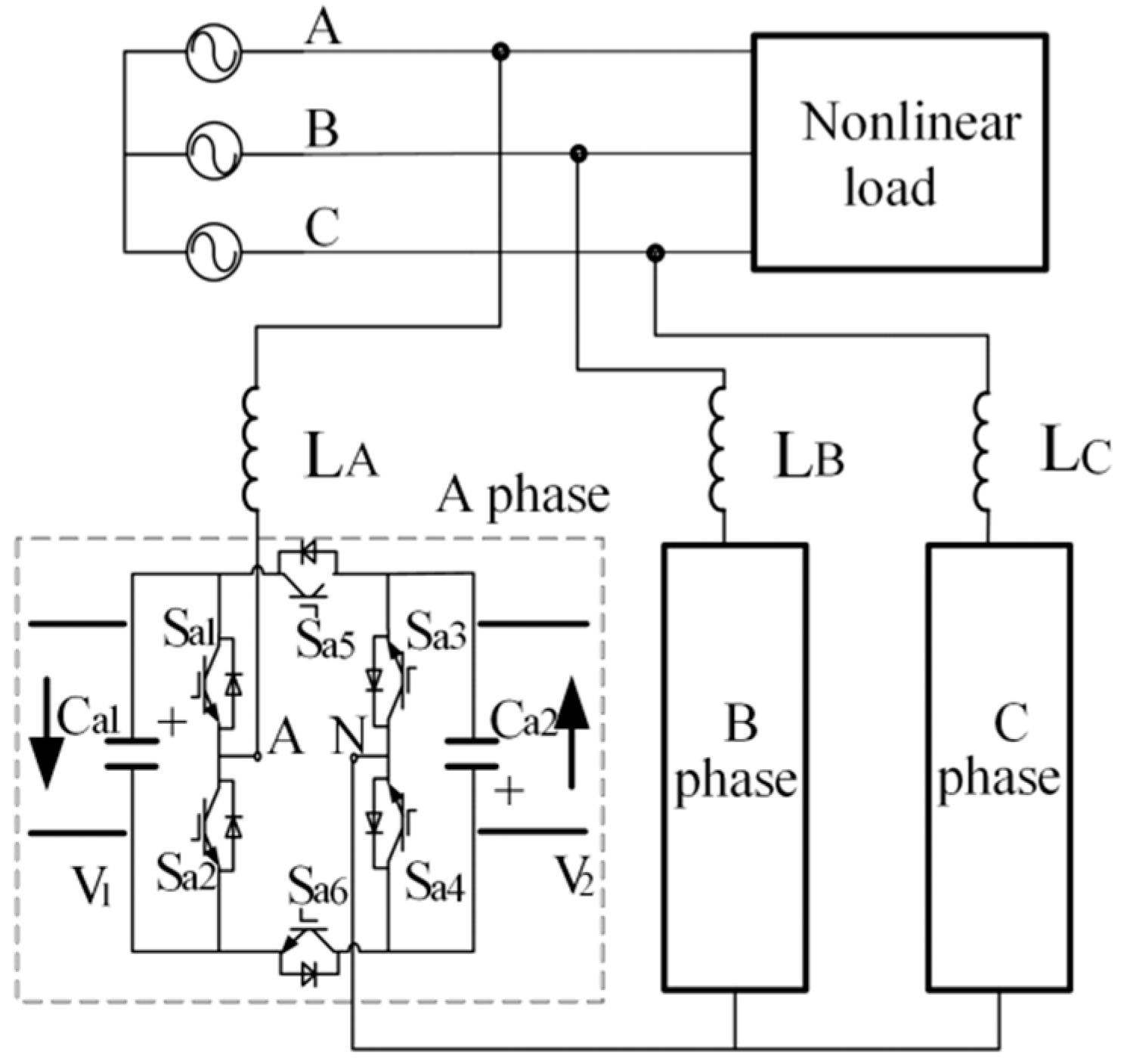
2. Analysis of the Novel Seven-Level Topology

2.1. The Structure and Working Mechanism of the Novel Seven-Level H-Bridge Topology

Figure 1 shows the main circuit of a novel seven-level APF. The three-phase units have the same structure; A phase contains six power switches Sa1Sa6 and two capacitors Ca1 and Ca2 which are called the seven-level H-bridge topology. As can be seen from the dotted box in Figure 1, when Sa1, Sa2 (or Sa3, Sa4) are simultaneously turned on, Ca1 (or Ca2) is short-circuited, so Sa1, Sa2 (or Sa3, Sa4) must work in a complementary state. In addition, when Sa5 and Sa6 are simultaneously turned on, Ca1 and Ca2 are also short-circuited, so Sa5 and Sa6 also work in a complementary state. As can be seen from Table 1, the novel topology has seven working states. Among them, Sa5 and Sa6 work at low frequency, which is consistent with the modulation wave frequency. The switching frequency of Sa1 and Sa2 is half of Sa3 and Sa4. V1 and V2 are the voltages of Ca1 and Ca2, respectively, V1 = 2V2. Inductors LA, LB, and LC connect the converter to the power grid, balance the voltage difference between the grid and the converter output, and perform reactive compensation or harmonic suppression.

2.2. Comparison with Other Seven-Level Structures

Table 2 shows the comparison of the novel topology with the traditional diode-clamped and cascaded seven-level converters, in which the number of power switches per phase is 6, 12, and 12, and the number of capacitors is 2, 6, and 3, respectively. It can be seen that the structure of the novel topology is simple, and reduces the system volume. At the same time, considering the withstand voltage limit, the novel topology is suitable for medium-voltage and low-voltage situations.

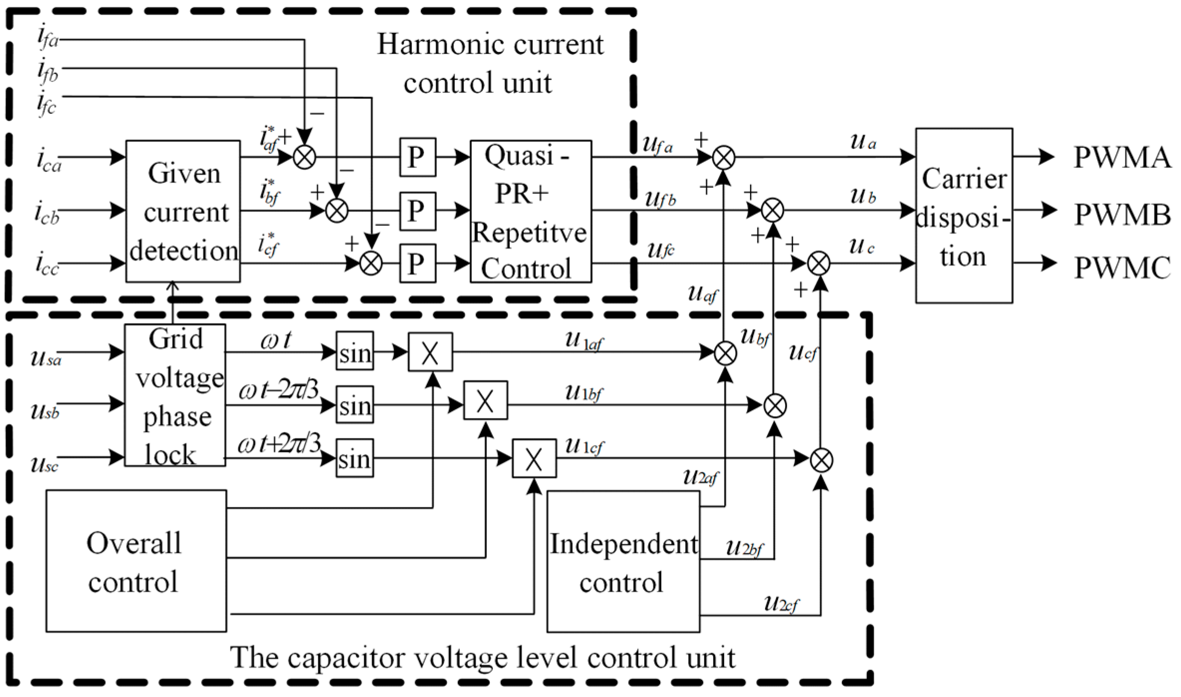
3. APF Control Method Based on Novel Topology Structure

3.1. Overall Control Strategy of the System

Figure 2 shows the diagram of the overall control structure of the novel APF system, including the harmonic current control unit and the capacitor-voltage stage control unit. In the harmonic current control unit, the output uf could be obtained based on the ipiq current detection method and quasi-proportional resonance (PR), repetitive control strategy. Considering that the imbalance of the capacitor voltage is caused by switch loss and drive pulse delay, the inverter output voltage is distorted, so the capacitor voltage must be regulated. Figure 2 shows the capacitor-voltage stage control unit, which uses a two-stage capacitor-voltage control strategy with overall control and independent control to obtain two-stage outputs u1f and u2f. Finally, the harmonic current control and the capacitor-voltage stage control are combined to obtain ua, ub, and uc. The carrier disposition is modulated to generate a pulse-width-modulated (PWM) signal, and the power amplifier drives the power switches to achieve harmonic suppression and capacitor-voltage regulation. The following cases, without loss of generality, are illustrated with the A phase as an example.

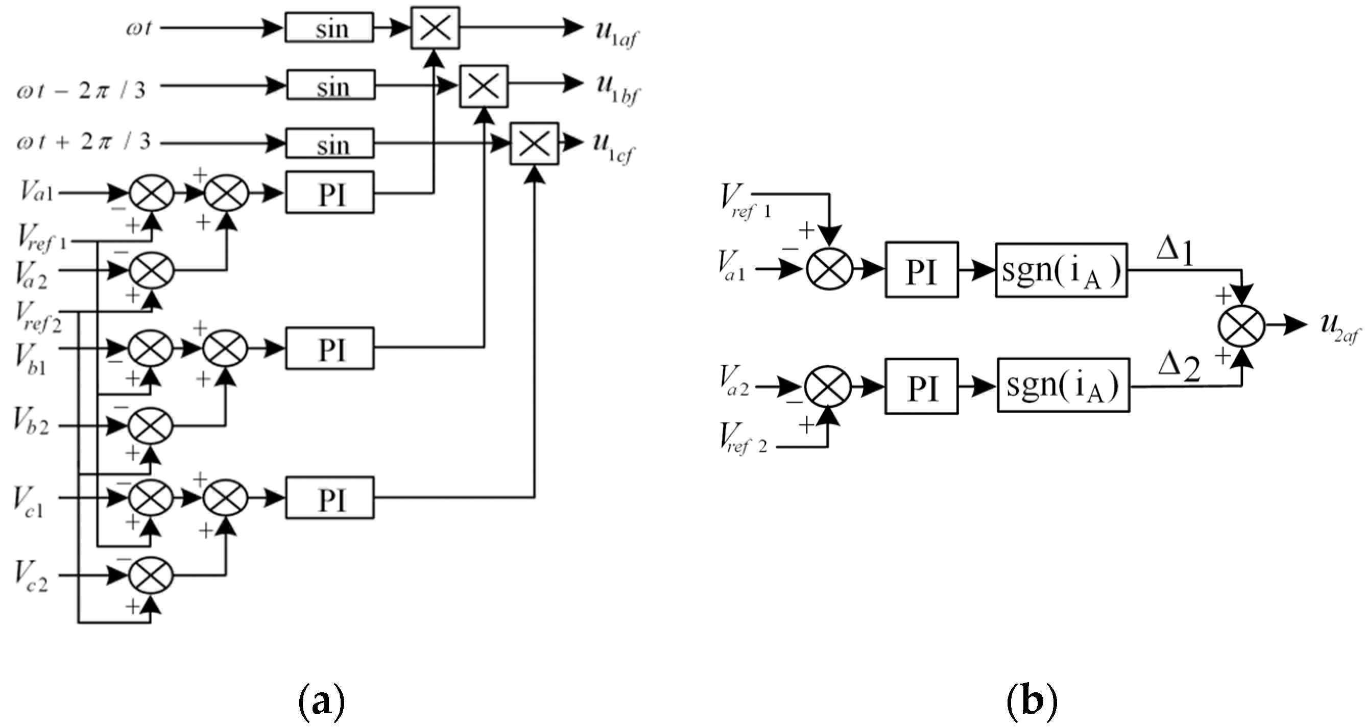
3.2. First-Stage Control Strategy of the Capacitor Voltage

The first stage is the overall control of capacitor Ca1 and Ca2, as shown in Figure 3a. Proportional integral regulator (PI) adjustment is performed for the sum of the given capacitor-voltage (Vref1 + Vref2) and the sum of the actual capacitor-voltage (Va1 + Va2). Its output is multiplied by the unit sine of the A-phase grid voltage to obtain the modulated wave u1af to realize the overall voltage control of the A-phase units Ca1 and Ca2, and obtain Vref1 + Vref2 = Va1 + Va2.

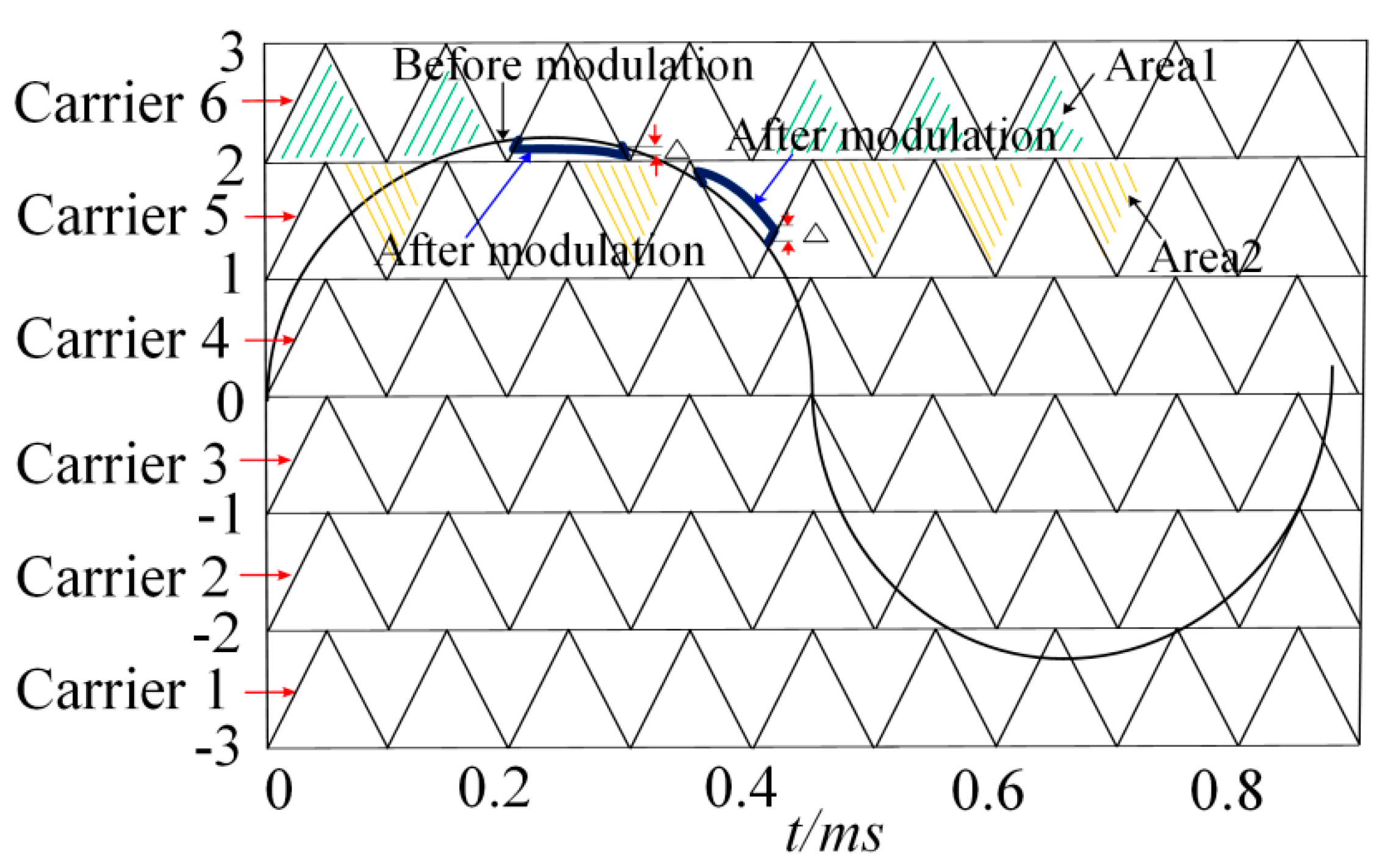
3.3. Second-Stage Control Strategy of the Capacitor Voltage

The second stage is the independent control of capacitors Ca1 and Ca2, as shown in Figure 3b, which consists of the determination of charge and discharge status and the control strategy of charge and discharge; sgn (iA) is the symbol function of iA.

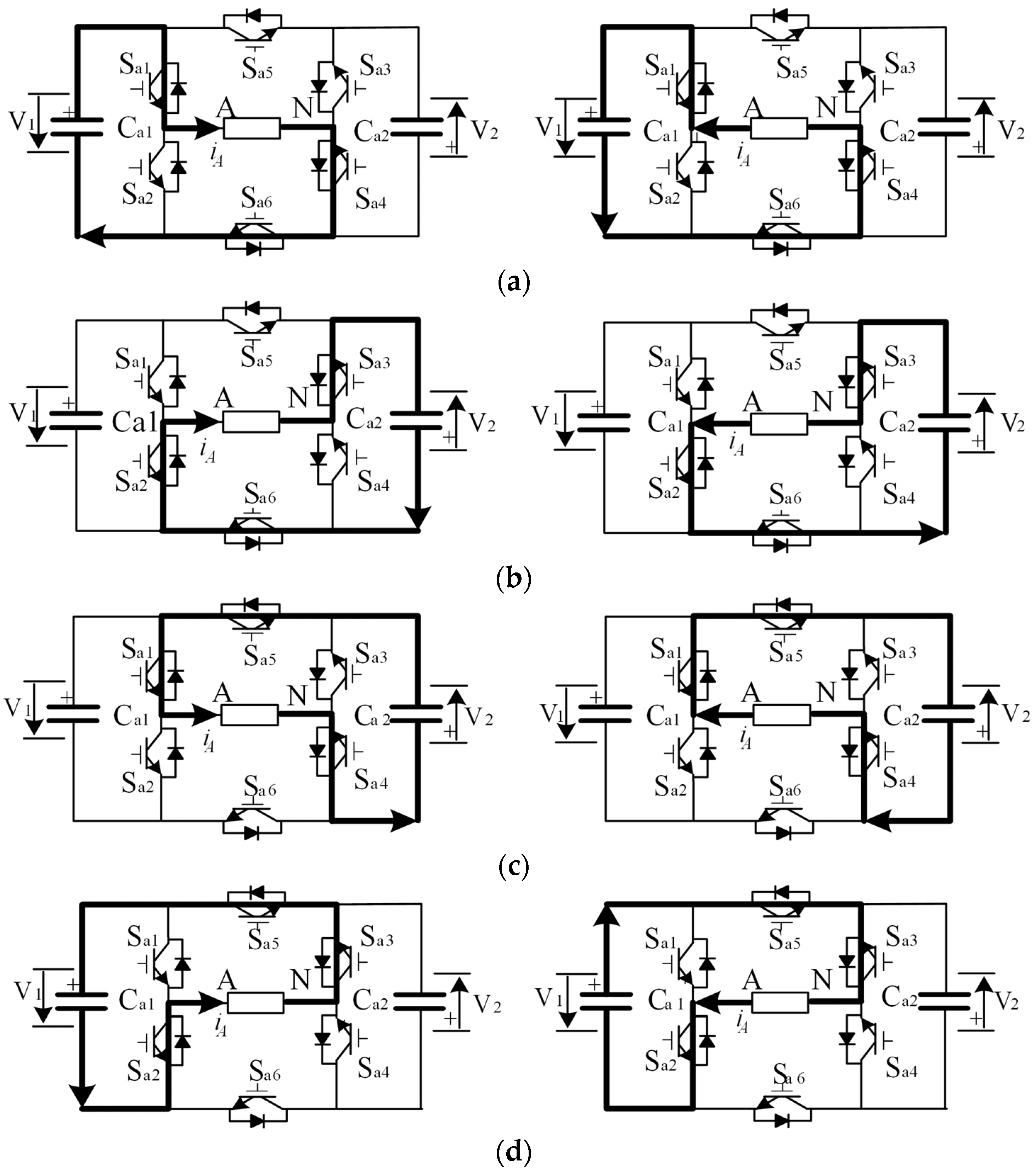
3.3.1. Determination of Charge and Discharge Status

Figure 4 shows the operating state of the unit circuit when Ca1 and Ca2 in the A-phase are charged and discharged, where iA is the output current. Table 3 gives the charge and discharge status of Ca1 and Ca2. First, the charge and discharge status of Ca1 and Ca2 are judged by the unit output status and the direction of iA. When the status is 1 or 7 (Table 3), if the charge and discharge of Ca1 and Ca2 are carried out, the output of the unit will change. At the same time, considering that Ca1 and Ca2 are suspended at state 4, the charge and discharge are not adjusted under these three conditions.

3.3.2. Control Strategy of Charge and Discharge

Figure 3b shows the charge and discharge control of Ca1 and Ca2. The actual voltage Va1, Va2 and the reference voltage Vref1, Vref2 are, respectively subjected to PI adjustment to obtain Δ1, Δ2, and U2af could be obtained after synthesis. Figure 5 shows a schematic diagram of the seven-level phase capacitor-voltage adjustment. The six-layer carriers output seven level states, which are defined as levels 1–7 from low to high. According to the carrier-disposition modulation principle, when the modulated wave is located in area 1 or 2, it outputs six levels (corresponding to V1 in Table 3). If the actual capacitor-voltage Va1 is greater than the reference voltage Vref1, reduction in the Va1 output could be achieved by increasing the discharging time of Ca1 or shortening the charging time of Ca1. When Ca1 is in a discharged state, if the modulated wave is compared with carrier 6 at that moment, the output is level 6 or level 7, if the amplitude of the modulated wave is decreased, and the output time of level 6 could be increased accordingly, that is, the discharge time of Ca1 is increased. Similarly, when Ca1 is in the charge state, the charging time of Ca1 could be reduced by changing the amplitude of the modulated wave. The voltage adjustment of Ca2 is the same as that of Ca1. It can be seen that the capacitor-voltage stabilization can be achieved by changing the amplitude of the modulated wave.

3.4. Parameter Calculation of Passive Elements

The larger the connected inductance value of APF is, the smaller the current ripple, but the smaller the rate of change of the compensation currens, and the weaker the current tracking ability. Secondly, the compensation current should be able to track the maximum rate of change of the command current. The smaller the inductance value is, the higher the rate of change of the current, and the faster the dynamic response speed of APF. However, the more drastic the current change is, the larger the ripple of the current. The DC side capacitor provides a stable DC power supply for the APF. The larger the capacitance, the more stable the DC side voltage. As the capacitor capacity increases, the volume and cost of the capacitor also increases.

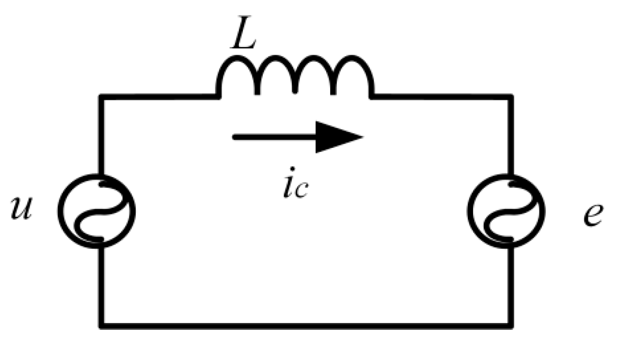
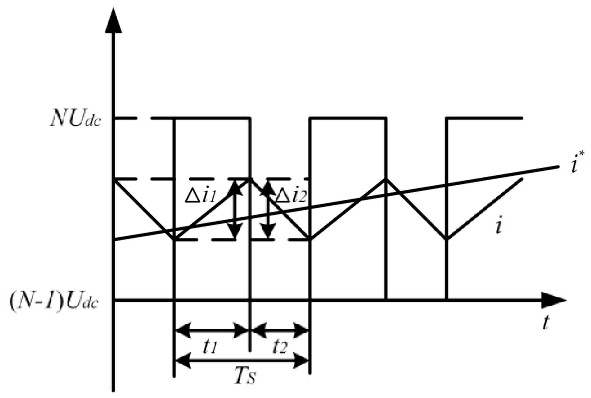
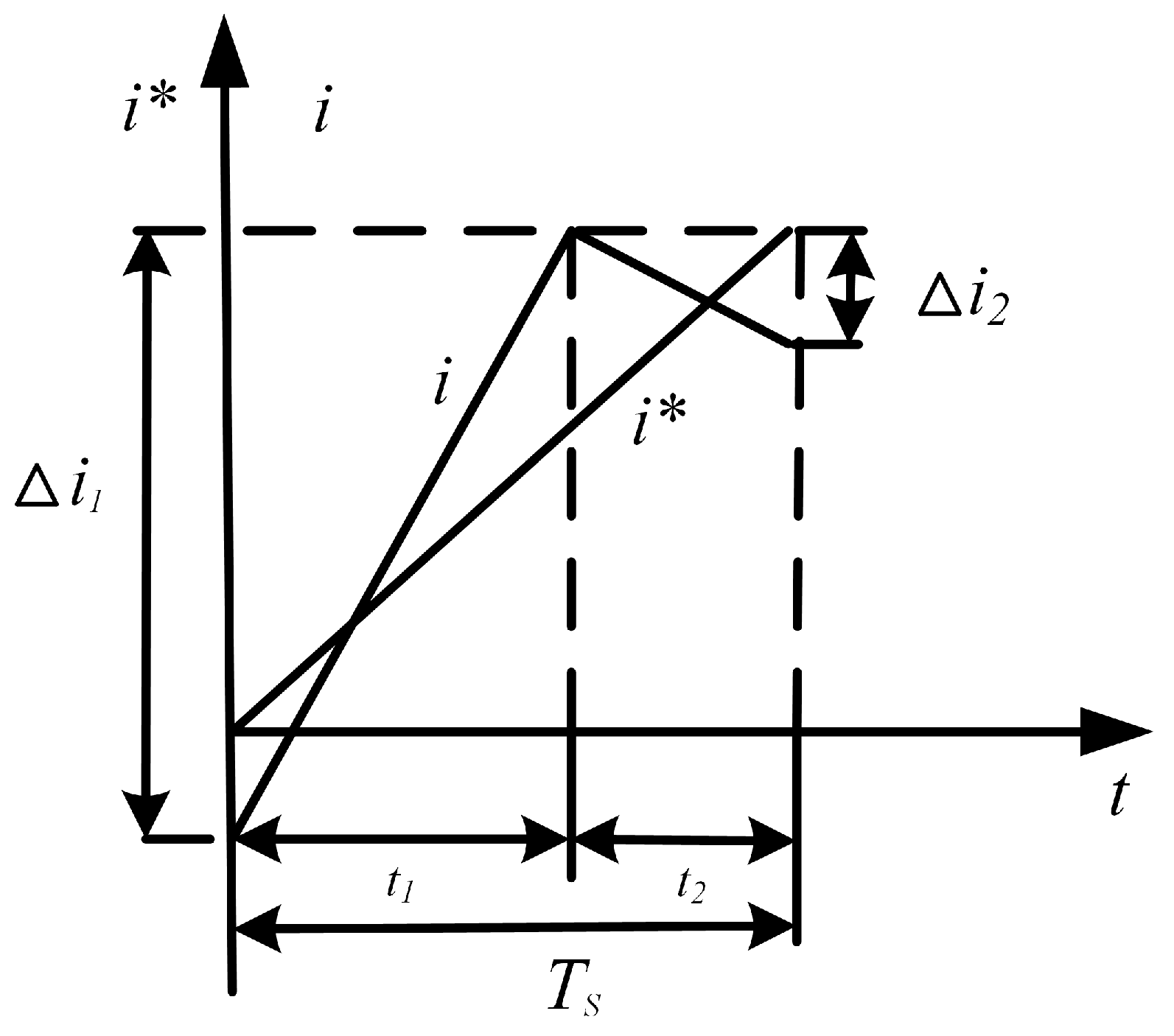
3.4.1. Parameter Calculation of Connected Inductor

a. Inductance parameter selection based on ripple constraint condition
The equivalent circuit of the APF device is shown in Figure 6, we can get:
u e = L d i c d t
where u is the AC side voltage of the inverter, e is the grid side voltage, L is the connection inductance, and ic is the compensation current.
In the process of the harmonic current compensation of APF, high-frequency harmonic components exist in the output of the AC side, which generates a ripple current under the action of inductance, and the ripple is the largest at the peak of the output current. Figure 7 shows, in a multilevel inverter, NUdc and (N–1)Udc levels are included at the peak output current of thr AC side. It is assumed that the high-level duration of NUdc is t1 and the low-level duration of (N–1)Udc is t2 in a switching period Ts, when the output current is at the peak, applying u = NUdc, dic/dt = Δic/Tc into Equation (1), we can get:
{ N U d c e = L Δ i 1 t 1 e ( N 1 ) U d c = L Δ i 2 t 2
When the output current is at the peak, it satisfies Δi1 = Δi2, t1 + t2 = Ts. Applying them into Equation (1):
t 1 = e ( N 1 ) U d c U d c T s
Δ i 1 = ( N U d c e ) [ e ( N 1 ) U d c ] L U d c T s
L = ( N U d c e ) [ e ( N 1 ) U d c ] Δ i 1 U d c T s
It can be seen from Equation (4) that increasing the connected inductance L can reduce the ripple current Δi1. In practical engineering, the ripple current usually takes 5% of the compensation current peak value. Thus, the lower limit of connection inductance could be obtained:
L ( N U d c e ) [ e ( N 1 ) U d c ] Δ i max U d c T s
In the Equation (6), fs = 20 kHz, N = 3, Udc = 130 V, e = 311 V, we can get:
L 1.55   mH
b. Inductance parameter selection based on the tracking ability of the compensation current at zero crossing
During one cycle of the command current, it changes the fastest at zero-crossing point (wt = 0), and the upper limit of the connected inductance could be determined according to the rate of change of the command current at zero. The current tracking waveform is shown in Figure 8. Δi1 and Δi2 are the current increments across the connected inductor during t1 and t2, and TS is a PWM switching cycle.
U d c e = L Δ i 1 t 1
e 0 = L Δ i 2 t 2
It can be seen from Equations (8) and (9) that the current has a maximum rate of change at the current zero-crossing point. When t1 = TS, t2 = 0, Δi2 = 0, Δi1 = Δi, e = 0, we can get:
d ( I m sin ω t ) d t | t = 0 = I m ω cos ω t | t = 0 = ω I m
U d c L max = ω I m
where Im is the current peak, we can get:
L max U d c ω I m
where Udc = 130 V, Im = 28.28 A, f = 50 Hz, w = 2πf, we can get:
L 14.6   mH
According to Equations (7) and (13), the value of the connected inductor LA, LB, and LC could be selected as 3 mH.

3.4.2. Parameter Calculation of Capacitor

The main considerations for the DC-side capacitors are: switching frequency fs, average value of DC bus voltage Udcavg, DC bus voltage ripple rate γv, and current peak Im.
The DC bus voltage ripple rate γv could be expressed as:
γ v = U d c max U d c a v g U d c a v g = U d c a v g U d c min U d c a v g
where Udcmax and Udcmin are the maximum value and the minimum value of the DC bus voltage, respectively.
From Equation (14), we can get:
U d c max = ( 1 + γ v ) U d c a v g
U d c min = ( 1 γ v ) U d c a v g
Since Q = it, Q = CU, there is:
Δ U d c max = U d c max U d c a v g = γ v U d c a v g = Δ Q C = 1 C T s I m
According to Equation (17), it could be inferred that the DC side capacitor C is:
C = 1 γ v U d c a v g T s I m = 1 γ v U d c a v g f s I m
where γv is 0.9%, fs is 20 kHz, Udcavg is 390 V, Im is 28.28 A, then C = 403 uF, the value of the capacitor Ca1 and Ca2 could be selected as 1000 uF.

4. System Simulation and Result Analysis

In order to verify the correctness and feasibility of the proposed topology, voltage-balance control strategy, and its application in the APF system, the following simulation is conducted. The parameters of the simulation are as follows: the voltage of the capacitor Ca1 Ud1 is 260 V, the voltage of the capacitor Ca2 Ud2 is 130 V, the grid frequency f is 50 Hz, he switching frequency fs is 20 kHz, and the inductance L is 3 mH.

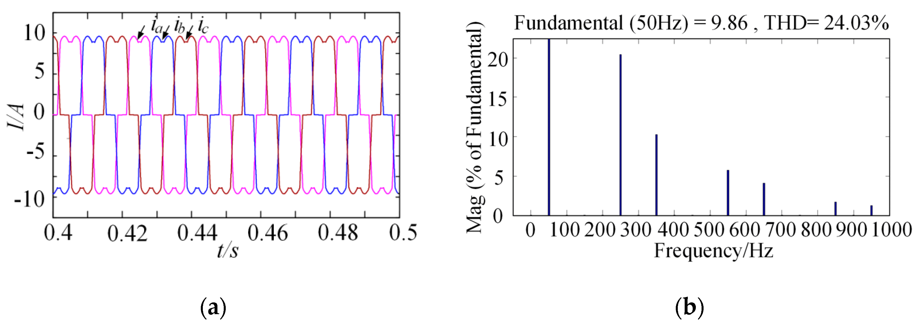
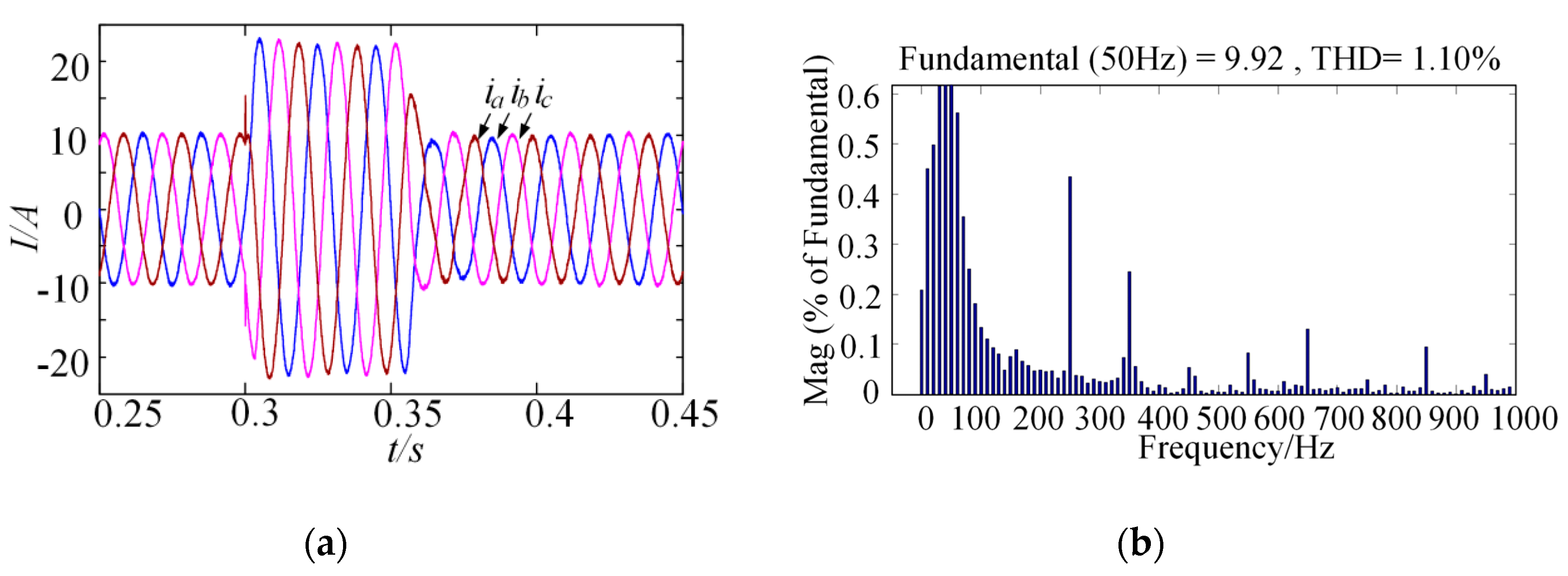
4.1. Under the Conditions of Balanced Grid and Load

The grid voltages UA, UB, and UC, are all 220 V, and the rectifier bridge is followed by the resistance of 40 Ω. Figure 9 and Figure 10 show the gird current in the A-phase and its THD before and after compensation, where the THD decreases from 24.03% to 1.10%. As shown in Figure 10a, before 0.3 s, the system load is a three-phase rectifier bridge with a resistance of 40 Ω, at 0.3 s, a resistance of 40 Ω is connected in parallel, and after 0.35 s, the load is changed to 40 Ω. It can be seen that in the case of a sudden change of load, the grid current fluctuates slightly, and tracks the reference input quickly, the voltage fluctuation is small, and there is no mutation substantially. Figure 11 shows the voltage of each capacitor, the fluctuation does not exceed 1 V, and it also shows the unit output, which is seven levels.

4.2. Under the Conditions of Unbalanced Grid and Load

The grid phase voltages UA, UB, and UC, are 220 V, 180 V, and 180 V, respectively. A single-phase rectifier load with a resistance of 10 Ω is connected between the A-phase and the B-phase, and the three-phase rectifier bridge is followed by a resistance of 40 Ω. Figure 12 and Figure 13 show the grid current and its current THD before and after compensation. It can be seen that the THD decreases from 20.98% to 1.89%, and the compensation effect is obvious. As shown in Figure 13a, before 0.3 s, the system load is a three-phase rectifier bridge with a resistance of 40 Ω, at 0.3 s, a resistance of 40 Ω is connected in parallel, and after 0.35 s, the load is changed to 40 Ω. It can be seen that in the case of a sudden change in system load, the grid current fluctuates slightly, and track the reference input quickly, the voltage fluctuation is small, and there is no substantial mutation. Figure 14 shows the voltage waveforms of each capacitor, which enter the steady-state at 0.05 s, and the fluctuation does not exceed 1 V, and it also shows the unit output of the novel power topology, which is seven levels.

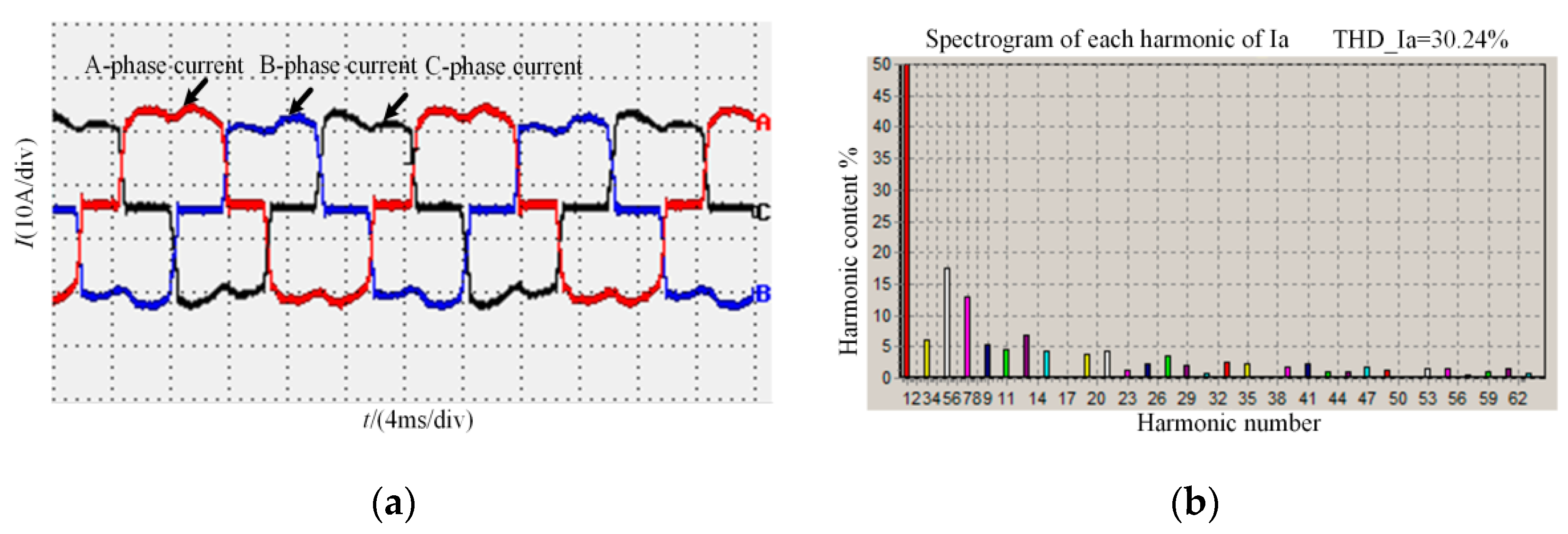
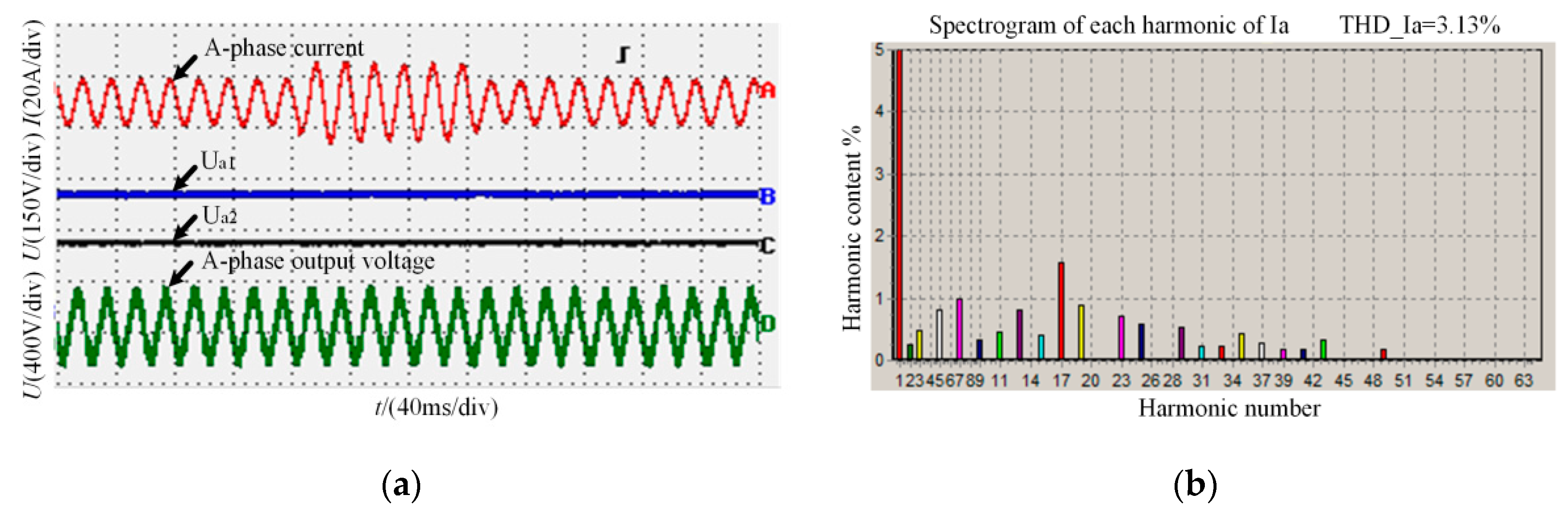
5. Experiment and Result Analysis

In order to verify the correctness and feasibility of the proposed topology, the voltage-balance control strategy, and its application in the APF system, the following experiment is conducted. Table 4 shows the parameters of the experiment, and the experiment system platform is shown in Figure 15.

5.1. Under the Conditions of Balanced Grid and Load

The grid phase voltages UA, UB, and UC, are all 220 V, and the rectifier bridge is followed by the resistance of 40 Ω. Figure 16 and Figure 17 show the grid current waveforms of the A-phase and its THD before and after compensation, where the phase current THD is reduced from 29.49% to 2.79%, and the compensation effect is obvious. At the same time, the dynamic compensation performance of the system was studied. The rectifier was connected with a 40 Ω resistance load, then a 40 Ω load resistance was connected in parallel, and finally removed. It can be seen from Figure 17a that Ua1 and Ua2 are stable at a reference value, and the system has good dynamic compensation performance if the power grid and load are all balanced, and it also shows the unit output of the novel power topology, which is seven levels.

5.2. Under the Conditions of Unbalanced Grid and Load

The grid phase voltages UA, UB, and UC are 220 V, 180 V, and 180 V, respectively. A single-phase rectifier load with a resistance of 10 Ω is connected between A phase and B phase, and the three-phase rectifier bridge is followed by a resistance of 40 Ω. Figure 18 and Figure 19 show the grid current and its current THD before and after compensation. It can be seen that the THD decreases from 30.24% to 3.13%, and the compensation effect is obvious. At the same time, the dynamic compensation performance of the system was studied. The rectifier was connected with a 40 Ω resistance load; then a 40 Ω load resistance is connected in parallel, and finally removed. It can be seen from Figure 19a that Ua1 and Ua2 are stable at a reference value, and the system has a good dynamic compensation performance if the power grid and load are all balanced, and it also shows the unit output of the novel power topology, which is seven levels.

6. Conclusions

This paper proposes a novel seven-level power topology. Compared to the novel seven-level topology, each power switch in a traditional two-level topology withstands the total DC bus voltage, while some power switches in the novel seven-level topology only withstand one-third of the total DC bus voltage; therefore, the novel seven-level topology has large power capacity, and reduces the withstand voltage of the power switches. The novel seven-level topology makes the output waveform closer to a sine wave by increasing the number of output levels and thereby improves the quality of the output waveform. According to the simulation and experimental results in this paper, the compensated grid current THD with the seven-level APF is only 1%–3%, much lower than the traditional two-level and three-level APF whose compensated grid current THD is usually greater than 5%, and the harmonic suppression effect is obvious. Compared to other seven-level topologies, the novel seven-level topology reduces the number of power switches and capacitors; thus reducing the size and cost of the device. Through the in-depth analysis of the working mechanism of the proposed topology, the engineering realization of the seven-level output is given. Besides, for the problem of capacitor-voltage imbalance in the application, an equalization control strategy with overall control and independent control of the two-stage capacitor voltage is proposed. In addition, the passive elements have been selected based on detailed mathematical analysis. Finally, from the above simulation and experimental work, we can see that the voltage control strategy described in this paper can achieve better cell capacitor-voltage regulation and the three-phase APF can achieve better compensation effect.

Author Contributions

H.G. conceived and designed the simulations and experiments; P.Z. analyzed the data; X.L. and S.F. wrote the paper; J.M. and R.L. checked the paper.

Funding

This research work was funded by the National Natural Science Foundation of China grant number 51177031 and the Science and Technology Planning Project of Guangdong Province of China(2016B010135001).

Conflicts of Interest

The authors declare no conflict of interest.

References

  1. Gadgune, S.Y.; Jadhav, P.T.; Chaudhary, L.R.; Waware, M.M. Implementation of shunt APF based on Diode Clamped and Cascaded H-bridge multilevel inverter. In Proceedings of the International Conference on Electrical, Computer and Communication Technologies (ICECCT), Coimbatore, India, 5–7 March 2015; pp. 1–7. [Google Scholar]
  2. Choi, W.; Lam, C.; Wong, M.; Han, Y. Analysis of DC link voltage controls in three-phase four-wire hybrid active power filters. IEEE Trans. Power Electron. 2013, 28, 2180–2191. [Google Scholar] [CrossRef]
  3. Hou, S.; Fei, J. Adaptive fuzzy sliding control with fuzzy sliding term for three-phase active power filter. In Proceedings of the IEEE International Conference on Control and Automation (ICCA), Hangzhou, China, 12–14 June 2013; pp. 1318–1323. [Google Scholar]
  4. Lam, C.; Wong, M.; Choi, W.; Cui, X.; Mei, H.; Liu, J. Design and performance of an adaptive low-DC-voltage-controlled LC-hybrid active power filter With a neutral inductor in three-phase four-wire power systems. IEEE Trans. Ind. Electron. 2014, 61, 2635–2647. [Google Scholar] [CrossRef]
  5. Alishah, R.S.; Hosseini, S.H.; Babaei, E.; Sabahi, M. Optimal Design of New Cascaded Switch-Ladder Multilevel Inverter Structure. IEEE Trans. Ind. Electron. 2017, 64, 2072–2080. [Google Scholar] [CrossRef]
  6. Zhu, H.; Shu, Z.; Gao, F. Five-level diode-clamped active power filter using voltage space vector-based indirect current and predictive harmonic control. IET Power Electron. 2014, 7, 713–723. [Google Scholar] [CrossRef]
  7. Banaei, M.R.; Jannati Oskuee, M.R.; Khounjahan, H. Reconfiguration of semi-cascaded multilevel inverter to improve systems performance parameters. IET Power Electron. 2014, 7, 1106–1112. [Google Scholar] [CrossRef]
  8. Babaei, E.; Laali, S.; Bayat, Z. A Single-Phase Cascaded Multilevel Inverter Based on a New Basic Unit With Reduced Number of Power Switches. IEEE Trans. Ind. Electron. 2015, 62, 922–929. [Google Scholar] [CrossRef]
  9. Chen, Z.; Wang, Z.; Li, M. A hybird cascade H-bridge seven-level converter for active power filter. In Proceedings of the IECON 2014—40th Annual Conference of the IEEE Industrial Electronics Society, Dallas, TX, USA, 29 October–1 November 2014; pp. 1041–1047. [Google Scholar]
  10. Boora, K.; Kumar, J.; Himanshu. A new general topology for asymmetrical multilevel inverter with reduced number of switching components. In Proceedings of the 2017 Recent Developments in Control, Automation & Power Engineering (RDCAPE), Noida, India, 26–27 October 2017; pp. 66–71. [Google Scholar]
  11. Hameed, U.; Ali, M.; Sadiq, H.; Khawaja, A.H.; Abdullah Khalid, H. Comparative study of Cascaded H-Bridge Multi-level Inverter using different Phase Shifted PWM Techniques. In Proceedings of the 2018 International Conference on Power Generation Systems and Renewable Energy Technologies (PGSRET), Islamabad, Pakistan, 10–12 September 2018; pp. 1–6. [Google Scholar]
  12. Singhai, S.; Pandey, A.; Singh, V. New Topology of Asymmtrical Multilevel inverter [15/29 Level]. In Proceedings of the 2018 International Conference on Current Trends towards Converging Technologies (ICCTCT), Coimbatore, India, 1–3 March 2018; pp. 1–6. [Google Scholar]
  13. Koshti, A.K.; Rao, M.N. A brief review on multilevel inverter topologies. In Proceedings of the 2017 International Conference on Data Management, Analytics and Innovation (ICDMAI), Pune, India, 24–26 February 2017; pp. 187–193. [Google Scholar]
  14. Sajedi, S.; Basu, M.; Farrell, M. New grid-tied cascaded multilevel inverter topology with reduced number of switches. In Proceedings of the 2017 52nd International Universities Power Engineering Conference (UPEC), Heraklion, Greece, 28–31 August 2017; pp. 1–6. [Google Scholar]
  15. Amamra, S.; Meghriche, K.; Cherifi, A.; Francois, B. Multilevel Inverter Topology for Renewable Energy Grid Integration. IEEE Trans. Ind. Electron. 2017, 64, 8855–8866. [Google Scholar] [CrossRef]
  16. Haji-Esmaeili, M.M.; Naseri, M.; Khoun-Jahan, H.; Abapour, M. Fault-tolerant structure for cascaded H-bridge multilevel inverter and reliability evaluation. IET Power Electron. 2017, 10, 59–70. [Google Scholar] [CrossRef]
  17. Mora, A.; Juliet, J.; Santander, A.; Lezana, P. Dead-Time and Semiconductor Voltage Drop Compensation for Cascaded H-Bridge Converters. IEEE Trans. Ind. Electron. 2016, 63, 7833–7842. [Google Scholar] [CrossRef]
  18. Dhanamjayulu, C.; Meikandasivam, S. Performance verific-ation of symmetric hybridized cascaded multilevel inverter with reduced number of switches. In Proceedings of the 2017 Innovations in Power and Advanced Computing Technologies (i-PACT), Vellore, India, 21–22 April 2017; pp. 1–5. [Google Scholar]
  19. Hasan, M.M.; Abu-Siada, A. A novel three phase cascaded multilevel inverter topology. In Proceedings of the 2016 IEEE Industrial Electronics and Applications Conference (IEACon), Kota Kinabalu, Malaysia, 20–22 November 2016; pp. 31–35. [Google Scholar]
  20. Kangarlu, M.F.; Babaei, E. A Generalized Cascaded Multilevel Inverter Using Series Connection of Submultilevel Inverters. IEEE Trans. Power Electron. 2018, 28, 625–636. [Google Scholar] [CrossRef]
  21. Srinivas, C.; PhaniSanthoshi, K.; AppaRao, G.V.; Siva, K.N.V. A Novel Seven Level Asymmetrical Inverter Topology to Reduce Total Harmonic Distortion. In Proceedings of the 2018 International Conference on Current Trends towards Converging Technologies (ICCTCT), Coimbatore, India, 1–3 March 2018; pp. 1–4. [Google Scholar]
  22. Ramya, D.; Mary Antony, A.S. A reconfigurable five/seven level inverter with reduced switching losses. In Proceedings of the 2017 International Conference on Computation of Power, Energy Information and Commuincation (ICCPEIC), Melmaruvathur, India, 22–23 March 2017; pp. 656–659. [Google Scholar]
  23. Yarlagadda, A.K.; Eate, V.k.; Babu, Y.S.K.; Chakraborti, A. A Modified Seven Level Cascaded H Bridge Inverter. In Proceedings of the 2018 5th IEEE Uttar Pradesh Section International Conference on Electrical, Electronics and Computer Engineering (UPCON), Gorakhpur, India, 2–4 November 2018; pp. 1–6. [Google Scholar]
  24. Guo, H.F.; Chen, M.; Cao, Y.; Ma, Q.D.; Ling, Z.B. Design of 2MW/10kV cascaded H-bridge power conversion system. In Proceedings of the 2014 International Conference on Power System Technology, Chengdu, China, 20–22 October 2014; pp. 3335–3340. [Google Scholar]
  25. Kawakami, N.; Ota, S.; Kon, H.; Konno, S.; Akagi, H.; Kobayashi, H.; Okada, N. Development of a 500-kW Modular Multilevel Cascade Converter for Battery Energy Storage Systems. IEEE Trans. Ind. Appl. 2014, 50, 3902–3910. [Google Scholar] [CrossRef]
  26. Townsend, C.D.; Summers, T.J.; Betzl, R.E. Impact of Practical Issues on the Harmonic Performance of Phase-Shifted Modulation Strategies for a Cascaded H-Bridge StatCom. IEEE Trans. Ind. Electron. 2014, 61, 2655–2664. [Google Scholar] [CrossRef]
  27. Angulo, M.; Lezana, P.; Kouro, S.; Rodriguez, J.; Wu, B. Level-shifted PWM for Cascaded Multilevel Inverters with Even Power Distribution. In Proceedings of the 2007 IEEE Power Electronics Specialists Conference, Orlando, FL, USA, 17–21 June 2007; pp. 2373–2378. [Google Scholar]
  28. Sochor, P.; Akagi, H. Theoretical and Experimental Compa-rison Between Phase-Shifted PWM and Level-Shifted PWM in a Modular Multilevel SDBC Inverter for Utility-Scale Photovoltaic Applications. IEEE Trans. Ind. Appl. 2017, 53, 4695–4707. [Google Scholar] [CrossRef]
  29. Alex Bao Zambra, D. Comparison of Phase-Shift and Step Wave Modulation Technique applied to Symmetrical Cascaded Multilevel Inverter. IEEE Lat. Am. Trans. 2013, 11, 1156–1162. [Google Scholar] [CrossRef]
  30. Ko, Y.; Andresen, M.; Buticchi, G.; Liserre, M. Power Routing for Cascaded H-Bridge Converters. IEEE Trans. Power Electron. 2017, 32, 9435–9446. [Google Scholar] [CrossRef]
Figure 1. Seven-level active power filter (APF) main circuit.
Energies 12 02997 g001
Figure 2. The overall control structure of the new APF system.
Energies 12 02997 g002
Figure 3. Control strategy of the capacitor voltage: (a) Overall control, (b) Independent control.
Energies 12 02997 g003
Figure 4. Circuit state during Ca1, Ca2 charge and discharge: (a) Level 6; iA > 0, iA < 0; (b) Level 5; iA > 0, iA < 0; (c) Level 3; iA > 0, iA < 0; (d) Level 2; iA > 0, iA < 0.
Energies 12 02997 g004
Figure 5. Unit capacitor-voltage regulator schematic.
Energies 12 02997 g005
Figure 6. The equivalent circuit of the APF device.
Energies 12 02997 g006
Figure 7. Current ripple at current peak.
Energies 12 02997 g007
Figure 8. Current ripple at the current zero-crossing point.
Energies 12 02997 g008
Figure 9. Before compensation: (a) Grid current; (b) Current Total Harmonic Distortion (THD).
Energies 12 02997 g009
Figure 10. After compensation: (a) Grid current; (b) Current THD.
Energies 12 02997 g010
Figure 11. Each capacitor-voltage and the A-phase output voltage waveform.
Energies 12 02997 g011
Figure 12. Before compensation: (a) Grid current; (b) Current THD.
Energies 12 02997 g012
Figure 13. After compensation: (a) Grid current; (b) Current THD.
Energies 12 02997 g013
Figure 14. Each capacitor-voltage and the A-phase output voltage waveform.
Energies 12 02997 g014
Figure 15. Experiment system platform.
Energies 12 02997 g015
Figure 16. Before compensation: (a) Grid current; (b) Current THD.
Energies 12 02997 g016
Figure 17. After compensation: (a) Grid current, two capacitor voltages, and the output voltage of the A-phase; (b) Current THD.
Energies 12 02997 g017
Figure 18. Before compensation: (a) Grid current; (b) Current THD.
Energies 12 02997 g018
Figure 19. After compensation: (a) Grid current, two capacitor voltages, and the output voltage of the A-phase; (b) Current THD.
Energies 12 02997 g019
Table 1. Switching states of the seven-level topology.
Switch StatusOutput Level
Sa1,Sa2Sa3,Sa4Sa5,Sa6
1,01,00,1+(V1 + V2)
1,00,10,1+V1
0,11,00,1+V2
1,0 or 0,11,0 or 0,11,0 or 0,10
1,00,11,0V2
0,11,01,0V1
0,10,11,0−(V1 + V2)
Table 2. Seven-level topology comparison.
StructureDiode ClampCascading H-BridgeNew Topology
Category
Topology Energies 12 02997 i001 Energies 12 02997 i002 Energies 12 02997 i003
Number of single-phase power switches12126
Number of single-phase capacitors632
Table 3. State determination of Ca1, Ca2 charge and discharge.
CurrentiA > 0iA < 0
Output Level
7: V1 + V2--
6: V1Ca1 discharge, Ca2 suspendCa1 charge, Ca2 suspend
5: V2Ca1 suspend, Ca2 dischargeCa1 suspend, Ca2 charge
4: 0--
3: −V2Ca1 suspend, Ca2 chargeCa1 suspend, Ca2 discharge
2: −V1Ca1 charge, Ca2 suspendCa1 discharge, Ca2 suspend
1: −(V1 + V2)--
Table 4. Main parameters of the system.
System ParametersValues
The voltage of capacitor Ca1260 V
The voltage of capacitor Ca2130 V
The capacitor Ca11000 uF
The capacitor Ca21000 uF
The switching frequency fs20 kHz
The grid frequency f50 Hz
The inductor LA, LB, LC3 mH
The balanced grid phase voltages UA, UB, UC220 V
The balanced resistance load R40 Ω
The unbalanced grid phase voltages UA, UB, UC220 V, 180 V, 180 V
A single-phase rectifier load RAB10 Ω

