Article

Assessment of the Impact of Stagnation Temperatures in Receiver Prototypes of C-PVT Collectors

Department of Construction, Energy and Environmental Engineering, Gävle University, 801 76 Gävle, Sweden
Energies 2019, 12(15), 2967; https://doi.org/10.3390/en12152967
Submission received: 30 April 2019 / Revised: 20 July 2019 / Accepted: 26 July 2019 / Published: 1 August 2019

Abstract

:
Concentrating Photovoltaic Thermal (C-PVT) solar collectors produce both thermal and electric power from the same area while concentrating sunlight. This paper studies a C-PVT design where strings of series-connected solar cells are encapsulated with silicone in an aluminium receiver, inside of which the heat transfer fluid flows, and presents an evaluation on structural integrity and performance, after reaching stagnation temperatures. Eight test receivers were made, in which the following properties were varied: Size of the PV cells, type of silicone used to encapsulate the cells, existence of a strain relief between the cells, size of the gap between cells, and type of cell soldering (line or point). The test receivers were placed eight times in an oven for one hour at eight different monitored temperatures. The temperature of the last round was set at 220 °C, which exceeds the highest temperature the panel design reaches. Before and after each round in the oven, the following tests were conducted to the receivers: Electroluminescence (EL) test, IV-curve tracing, diode function, and visual inspection. The test results showed that the receivers made with the transparent silicone and strain relief between cells experienced less microcracks and lower power degradation. No prototype test receiver lost more than 30% of its initial power, despite some receivers displaying a large number of cell cracks. The transparent and more elastic silicone is better at protecting the solar cells from the mechanical stress of thermal expansion than the compared silicone alternative, which was stiffer. As expected, larger cells are more prone to develop microcracks after exposure to thermal stress. Additionally, existing microcracks tend to grow in size relatively fast under thermal stress. EL imaging taken during our experiment leads us to conclude that it is far more likely for existing cracks to expand than for new cracks to appear.

1. Introduction

Photovoltaic thermal (PVT) solar panels produce both thermal and electric power from the same area. Combining solar thermal and photovoltaic production can be a way to increase the efficiency of silicone cells by reducing the working temperature through active cooling [1,2,3,4].
Additionally, the concentration has the potential to allow cost reduction by decreasing the receiver size in the panel. In fact, according to Giovinazzo et al., the biggest advantage of this type of collector design is to decrease material cost by reducing the amount of expensive components utilized such as solar cells, thermal receiver and/or selective surface [1].
This way, combining concentration with PVT (C-PVT) can also prove to be advantageous. However, concentrating does not only bring advantages. For non-tracking PVT collectors, one disadvantage is the longitudinal shading caused by the frame or the absence of reflector at larger solar incidence angles. This can have a very large impact, particularly on the electrical performance, if measures such as placing extra diodes are not taken [3].
Apart from performance and cost, another key aspect in solar collectors design is durability. Solar collectors must survive 20 years outdoors in order for the owners to be able to profit from the installation and this carries implications in terms of UV and temperature resistance. The stagnation temperature of a collector is reached when the heat losses are equal to the energy received from the sun [5,6,7]. This basically means that all incoming solar radiation is transferred to the surrounding environment either as heat losses or as optical losses. A particularly important disadvantage of concentration is the increase of the stagnation temperature, which can cause damage to the materials of the collector, in particular to the solar cells [1]. This issue will be covered in detail in this paper, namely, the survivability of the solar cells under stagnation conditions.
Hot-spots are a commonly known problem in PV panels that can lead to module failure [8,9,10,11] with much attention being given by researchers to developing methods for non-intrusive detection and prevention of hot-spots [10,11]. Extensive research has also been carried out on optimal power point tracking under shading or differential light conditions [11,12] and in the reduction of the impact of shading in the electrical output [3]. PVT panels have the ability to cool down the solar cells and, thus, the PV cells are not exposed, on a daily basis, to the same level of temperature variation as a PV panel. Since this temperature variation carries an inherent thermal stress, cooling the cells is expected to increase the longevity of the solar cells [1]. However, in the event of a system malfunction, such as pump failure, stagnation temperatures can be reached in a PVT, which means that the materials in these collectors either need to be able to withstand the stagnation temperatures, or there must be a system in place to prevent reaching stagnation, such as a tracker that moves away from the sun [3]. Either way, although PVT have less risk of hot-spot formation due to the heat extraction, this is still possible. It is important to mention that hot-spots are more problematic in concentrating PV or PVT panels, since stagnation temperature is generally higher than in a non-concentrating PV or PVT panels [1].
The most critical part in the manufacture of the PVT collector is the receiver [13,14]. A major technical design difficulty for PVT collectors is to find a material for encapsulating the solar cells that is able to effectively conduct the heat from the solar cells to the receiver while still maintaining a number of critical characteristics such as high electrical insulation, high transparency, low cost, ability to cope with thermal stress in order to protect the solar cells, resistance to moisture penetration, resistance to UV, and achieve a durability of 20 years or more. This difficulty is even more severe in C-PVT, since they face higher stagnation temperatures.
The electroluminescence test (EL) is a powerful tool commonly used to control the quality of the PV cell strings which is used by both research and industry [15,16]. Using this technique, it is possible to identify defects that are not visible to the naked eye such as microcracks and black (or so called “dead”) areas. These two defects are the principal cause of power losses in the cell strings, a fact which can be confirmed in the IV-Curve test. [16]
A C-PVT prototype collector was designed to produce 240 W (electricity) and 1250 W (thermal). An installation with eight prototype C-PVT collectors was carried out. The collectors were found to produce only 1200 W (el) directly after being installed. One day later, during which the stagnation temperature was reached, the production was found to have degraded significantly to 200 W (el). This incident highlighted to the authors the importance of the impact of stagnation temperatures in the performance of C-PVT collectors. This paper evaluates potential solutions to the mechanical stress induced by the thermal expansion caused by reaching stagnation temperature.
Problems with the manufacturing process of the prototypes, in particular, with the manual solar cell soldering, account for the difference between the installation expected electrical output of 1920 W and the initial measured electrical output of 1200 W. Such issues can easily be eliminated by automation of the cell soldering process with an automatic tabbing stringer machine, which the production company accomplished following the discovery of the above mentioned issue, and are thus not analyzed in the paper. However, a more important issue that was highlighted with this prototype installation, consisted in the post-stagnation electrical power reduction. A number of hypotheses on the possible reasons for this decrease, such as the encapsulation silicone or the intermetallic compounds, have been identified. A set of tests was designed with the goal of gathering data to evaluate each hypothesis.
This paper builds upon the work of Gomes et al. presented at the Solar World Congress in 2015, which presented an early evaluation of the impact of stagnation in PVT receivers [17]. Although addressing a relevant and novel topic for the construction of PVT receivers, this preliminary work required further clarification on points such as: ensuring the repeatability of the protocol by fully detailing the method and the equipment; presenting in a clear manner vital information such as the collector parameters and adding a section on the calculation of the stagnation temperature; a more in depth discussion of the results, namely by expanding the analysis of the thermal stress test results and adding a section on the evaluation of microcracks under electroluminescence; the introduction was also expanded with several new references to more adequately portray the state-of-the-art in PVT collectors and the use of EL methods.
This paper presents a novel study on tackling thermal stress challenges in C-PVT collectors using silicone-based encapsulation techniques.

2. Materials and Method

2.1. Description of the Prototype Collector and the Properties of Its Components

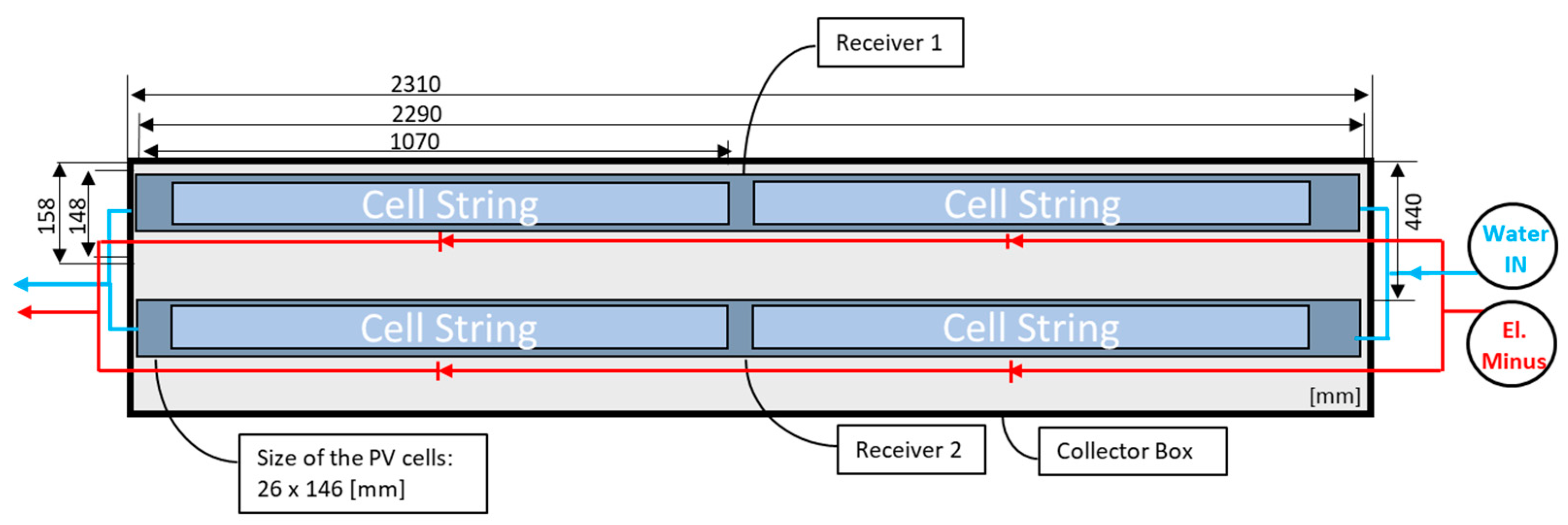
Figure 1 shows a schematic of the prototype collector viewed from the top, while 
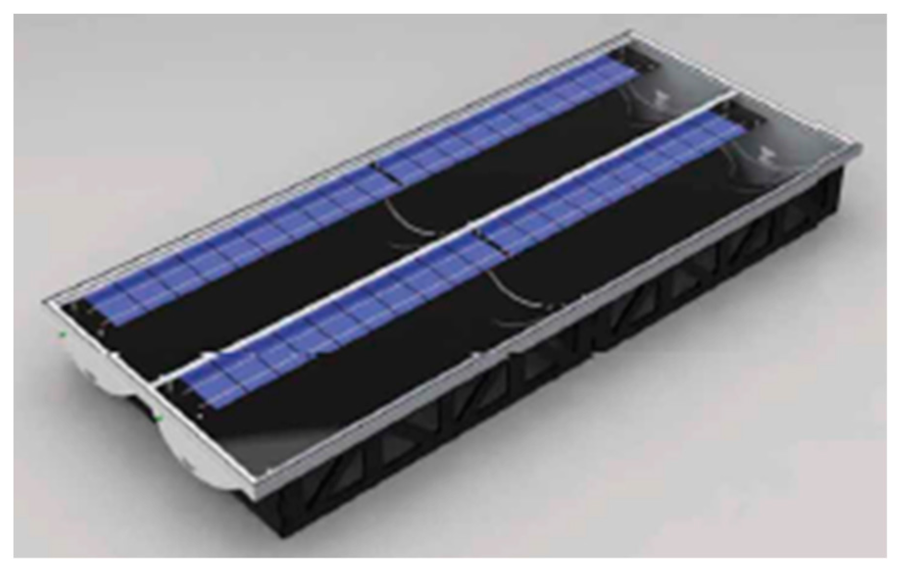
Figure 2 shows an image of the actual prototype. The total size of the collector is 2.31 × 0.955 m. The length of the thermal receiver is 2.290 m and the height is 0.158 m.
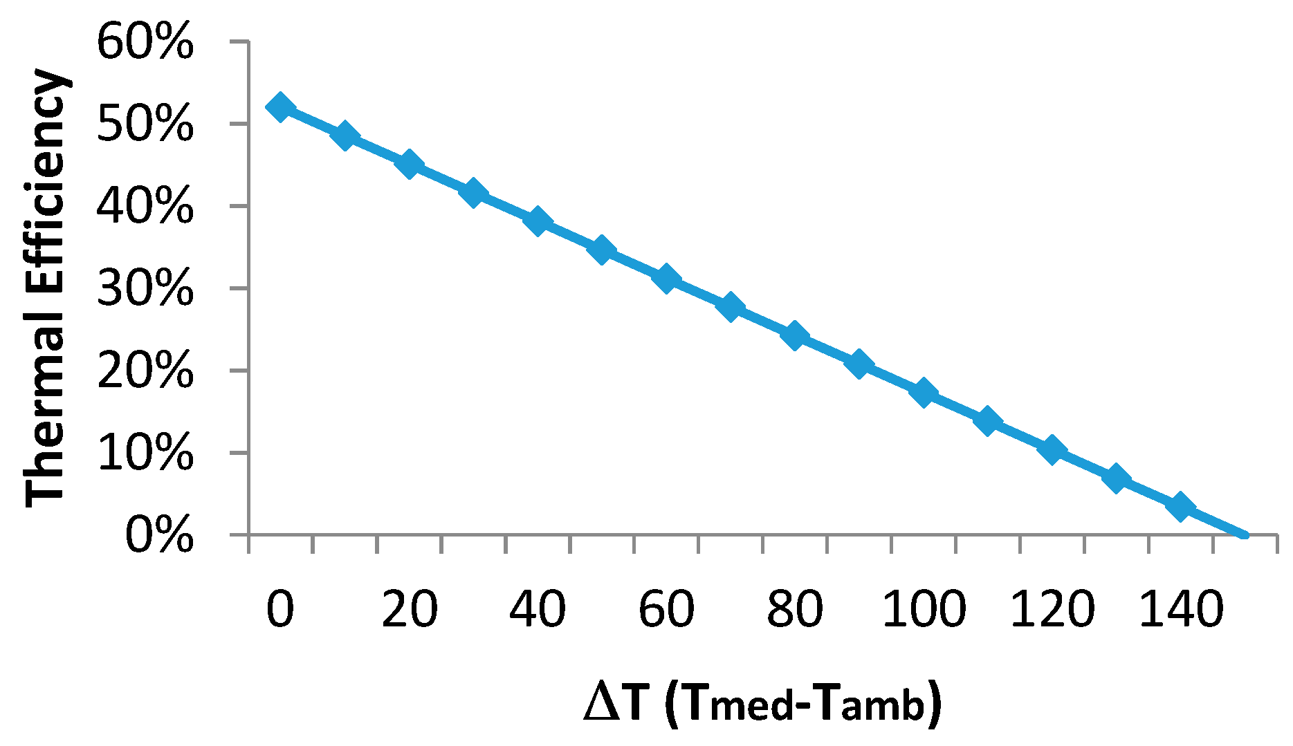
The manufacturer specifies an overall thermal efficiency of 52%. Furthermore, the linear loss coefficient a is 3.47 W/(m2K) [18]. Furthermore, the temperature dependence electrical coefficient has been tested by Bernardo et al. and found to be 0.4%/K. [2]
The following list shows some of the key components of the prototype collector:
Reflector: The reflector geometry of the prototype collector was initially developed by the Swedish company Vattenfall AB. The design is called Maximum Reflector Concentration (MaReCo), which belongs to a family of stationary reflectors patented by the company Solarus Sunpower AB. The reflector is composed of a compound parabolic and circular reflective that concentrates the solar radiation onto the receiver. Adsten et al. describe the geometry in full detail [19,20]. The reflector is purchased from Almeco and has a total solar reflectance ρtotal of 95%.
Receiver: The receiver is an aluminium extrusion that is 2.29 m long. A maximum expansion of 8mm has been calculated for a temperature variation between −20 °C and 150 °C based on linear temperature expansion. Solar cells and silicone are laminated on both sides of the receiver with one side facing the receiver and one side facing the reflector.
Cell encapsulation and Silicone: Cell encapsulation is done with two layers of silicone purchased from Wacker. A bottom layer of 0.5 mm that located between the receiver aluminium core and the solar cells and a top layer of 1 mm located between the solar cells and the air inside the collector box. In the prototypes created for the tests, two types of silicone gels are used:
  • A highly transparent and electrically insulating silicone (Elastosil 3201), which can be used both for the top layer and bottom layer. Thermal conductivity is 0.2 W/mK.
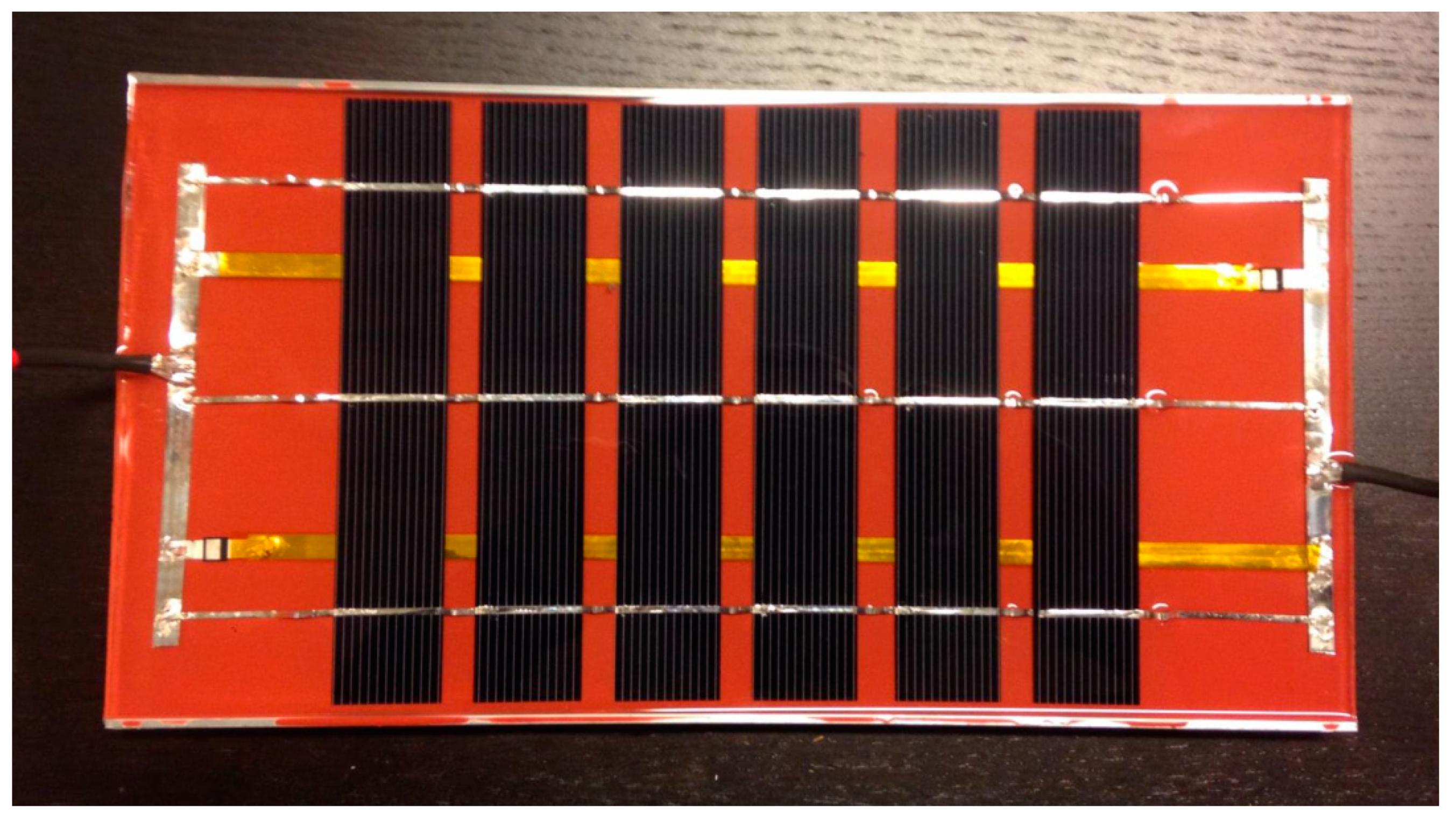
  • A reddish brown silicon (RT 740) that has the same electrical insulation properties as 3201 but has an improved thermal conductivity 0.5 W/mK which would allow more heat to be transferred from the cells to the receiver over the thin layer of silicon. It is important to note that this silicone can only be used in the bottom layer since it is not transparent and if used on the top layer would block the sunlight from reaching the cells. Another important point is that the red silicone is considerably stiffer than the transparent silicone, and thus transmits more thermal stress to the cells when the receiver experiences thermal expansion.
Standard Solar Cells: Each receiver side has two strings of 38 PV cells connected in parallel. Each receiver has two sides with cells: (a) the front side, which faces the glass, and (b) the back side, which faces the reflector. For the receivers tested in this paper, two cell sizes were used: (a) 28 × 148 mm and (b) 52 × 148 mm. A prototype C-PVT collector using cells with 52 × 148 mm would have 152 cells in total. These cells were laser cut in order to obtain these sizes. The goal of cutting the cells is to lower the current though the cell, which is specifically important for concentrating collectors.
Cell interconnecting Copper Ribbon: This is the small copper strip that connects the solar cells. In the industry, it is commonly called cell ribbon. Ribbon dimension is 1.6 mm × 0.2 mm with a total thickness of 0.2 mm. The coating of the ribbon is composed of 96.5% Tin and 3.5% Silver with a thickness varying between 16 and 24 µm. Yield strength is 90 N/mm2 (max), tensile strength is 210/mm2 (max) and elongation is 25% (minimal) According to the manufacturer (Ulbrich), this ribbon has a melting temperature of 220 °C.
Glass: The module contains a glazed protection which is made of SunArc low iron glass with a solar weighted transmittance τglass of 95%.

2.2. Description of the Implications of the Stagnation Temperature for the C-PVT Prototype Collectors

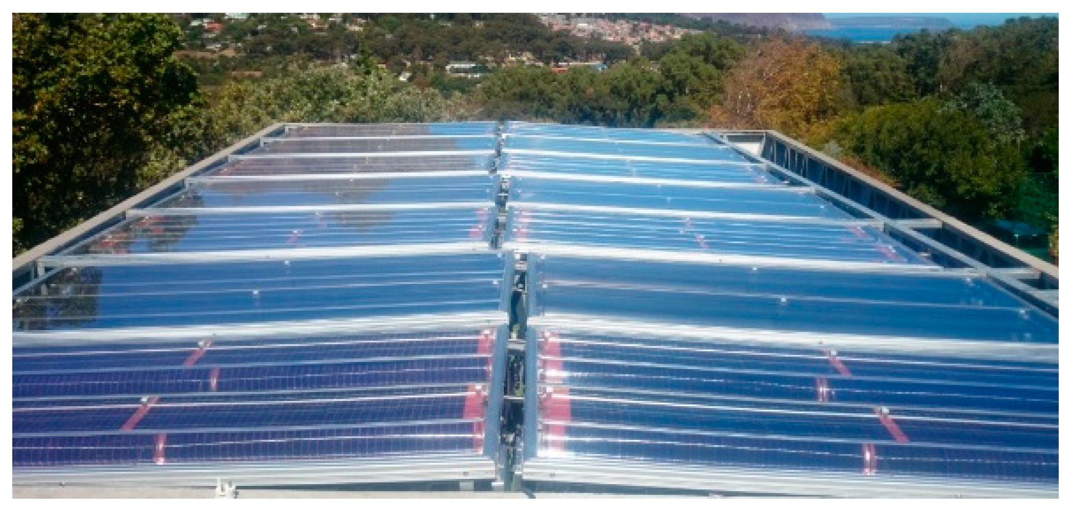
Eight C-PVT collectors and six concentrating thermal (T) collectors were installed in a warm country as show in Figure 3. The eight C-PVT collectors were connected to eight micro-inverters. Four thermal loops were connected to a central tank. Three of these loops contained two PVTs and two Ts while one loop contained only two PVT collectors.
The water outlet was not connected in the first day, when the collector was uncovered. Since it was a very sunny and warm summer day, this implies that the collector has reached stagnation temperature, which has been calculated to be around 180 °C.
The electrical power of this prototype installation was monitored. After the first hour of exposure to sunlight without cooling, the combined output of the eight PVT’s was found to be only 1200 W instead of the expected 1920 W. In the following day, also at peak sun, the electrical production of the installation was again measured and it had been greatly reduced to only 200 W.
The above measurements highlight two serious issues with this prototype installation:
  • The first concerns the measured electrical output of 1200 W, which is well below the 1920 W that would be expected according to the datasheet supplied by manufacturer where each of the eight collectors produces 240 W. This output decrease is likely to originate in the manufacturing process. The company that produced the prototypes is not only aware that this decrease is caused by the manual hand soldering process as they have also solved this issue by purchasing of an automatic tabbing stringer machine.
  • The second and most important issue is the reduction of the electrical power from 1200 to 200 W that the installation displayed in the second day, after cooling down and reaching stagnation again. This second issue is certainly not due to the manufacturing process but to the actual collector design and material selection. It is also important to mention that this power reduction is not so pronounced, if high temperatures are not reached, as shown by other tests.
Four hypotheses on the possible reasons for this large decrease (from 1200 to 200 W) have been identified and are described below:
  • The diodes broke down due to the high temperature.
  • The thermal expansion of the copper cell ribbon has damaged the cells.
  • The thermal expansion of the aluminium receiver has damaged the cells.
  • The high stagnation temperature has caused the copper ribbon to unsolder, cutting the electrical path to the inverter.
The thermal part of the C-PVT installation was not negatively affected in any way by stagnation. No water leaks were found, as well as no reduction in thermal power output. In fact, a slight thermal output increase has been measured, since the solar cells stopped converting the incoming solar irradiation into electricity and that solar radiation became heat instead.

2.3. The Prototype Receivers

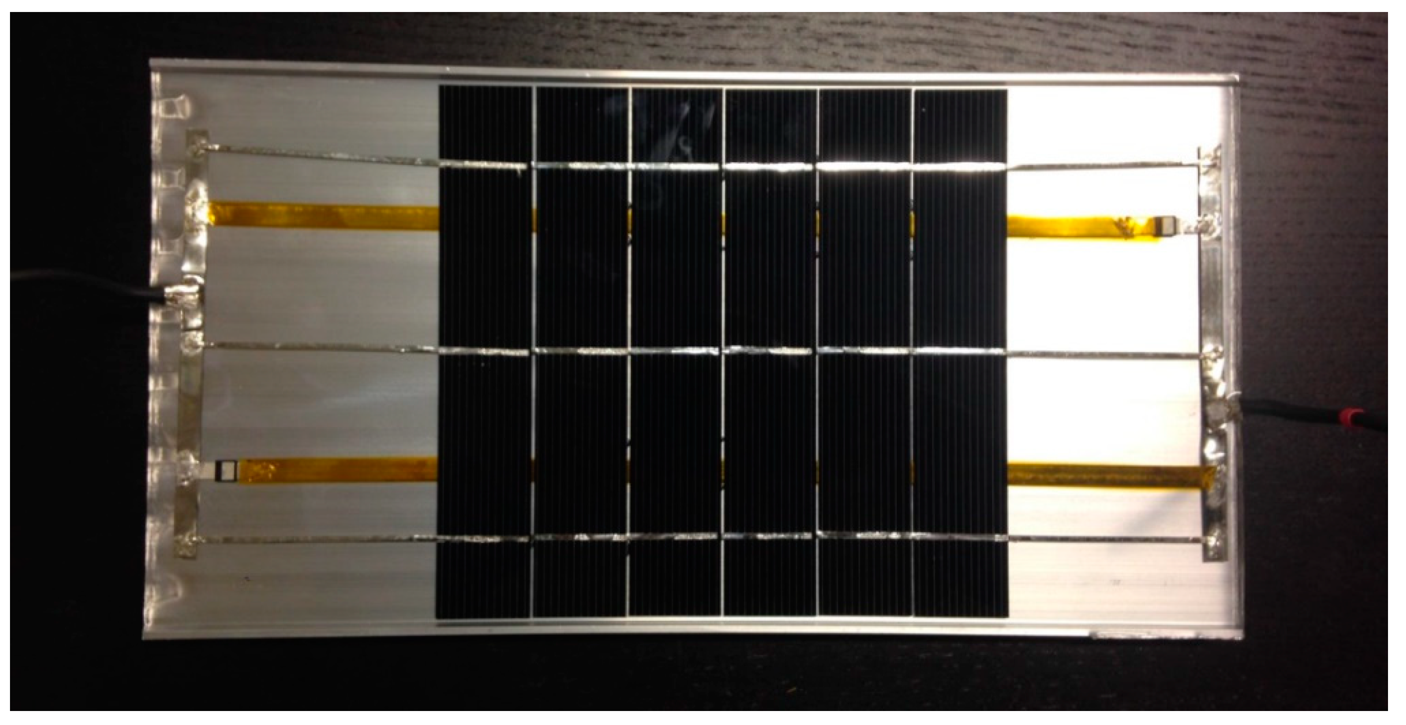
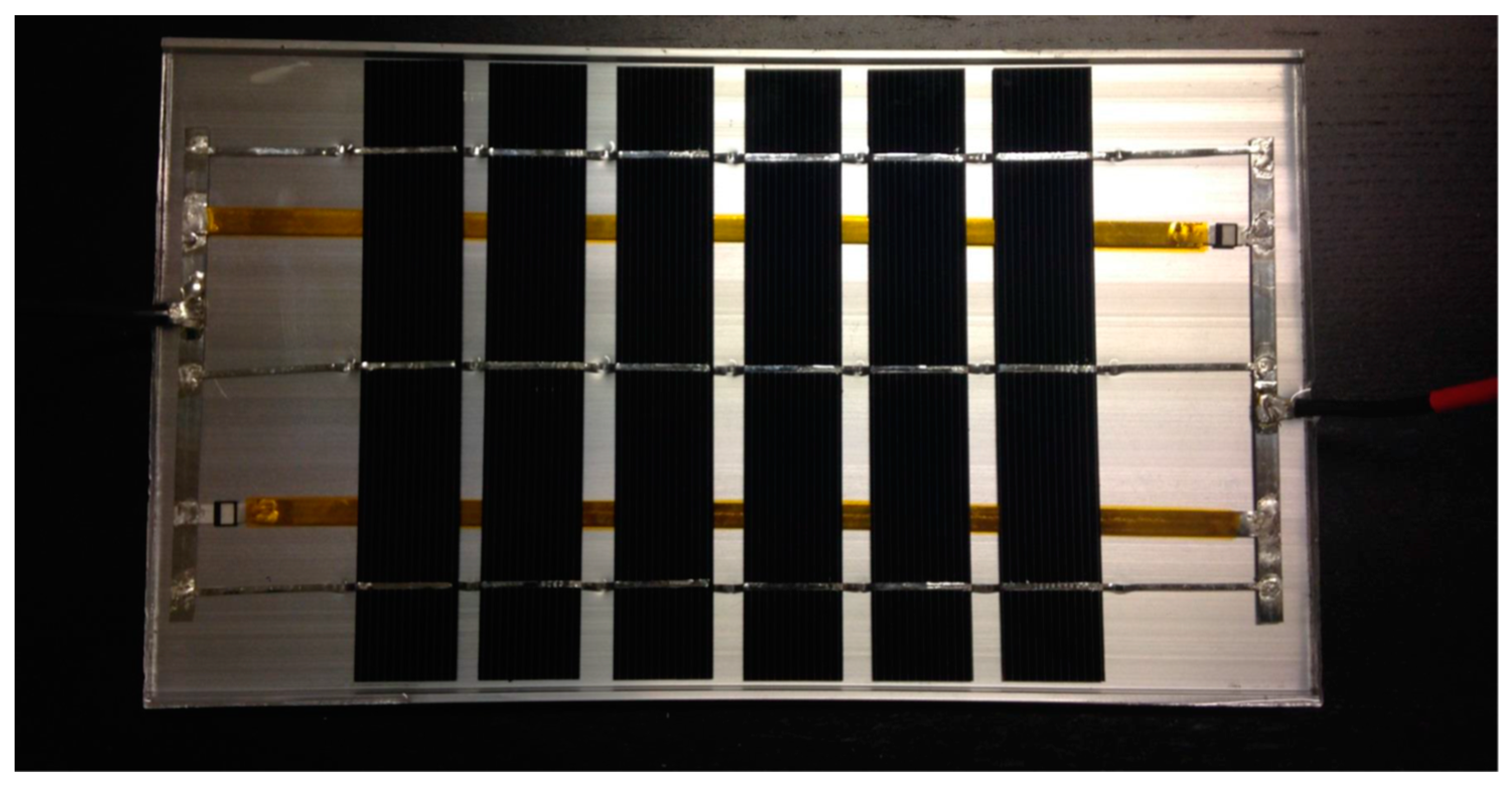
In order to discover the cause of the electrical performance reduction, eight prototype small receivers were manufactured at the company that made the prototypes C-PVT in the installation. Table 1 summarizes the characteristics of each small receiver. 
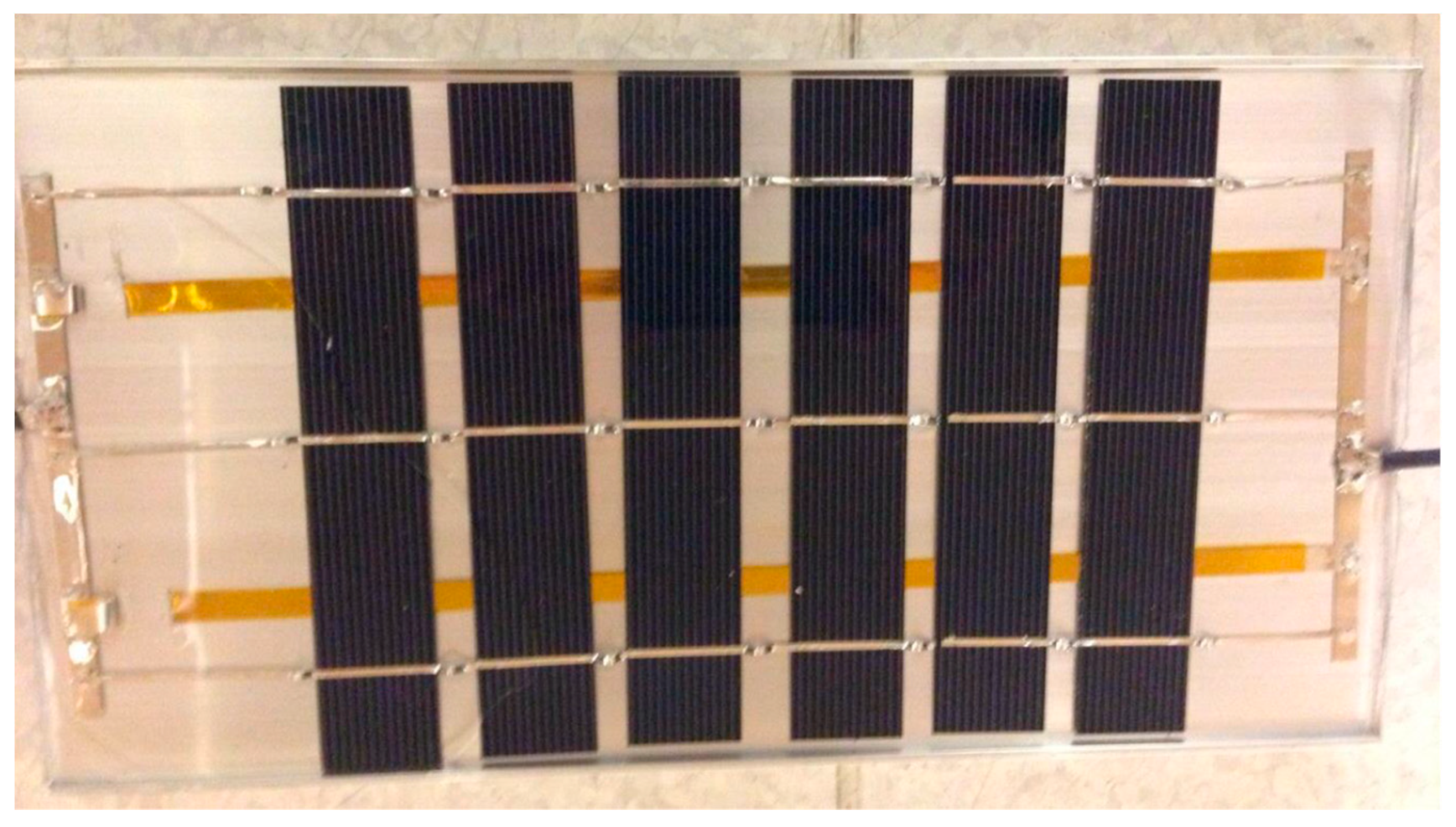
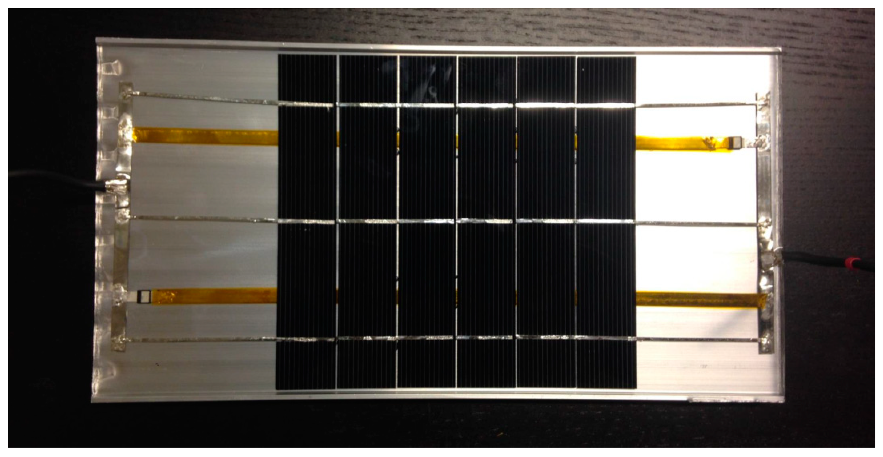
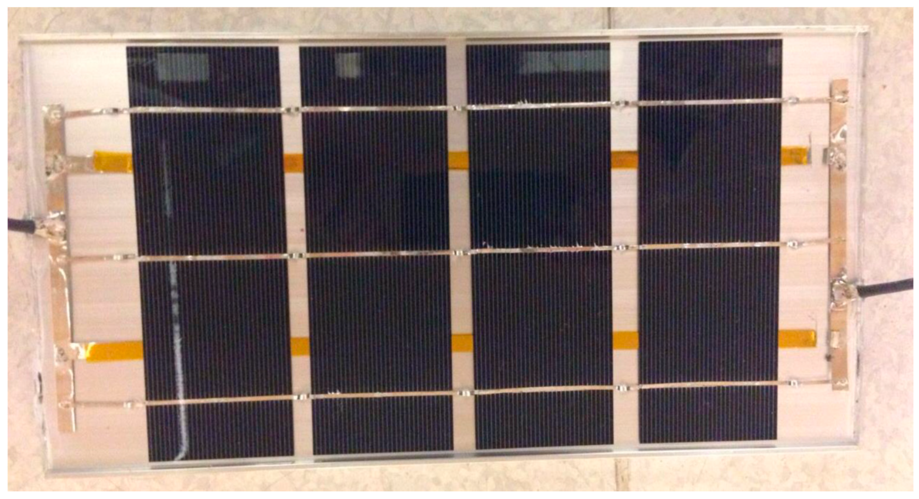
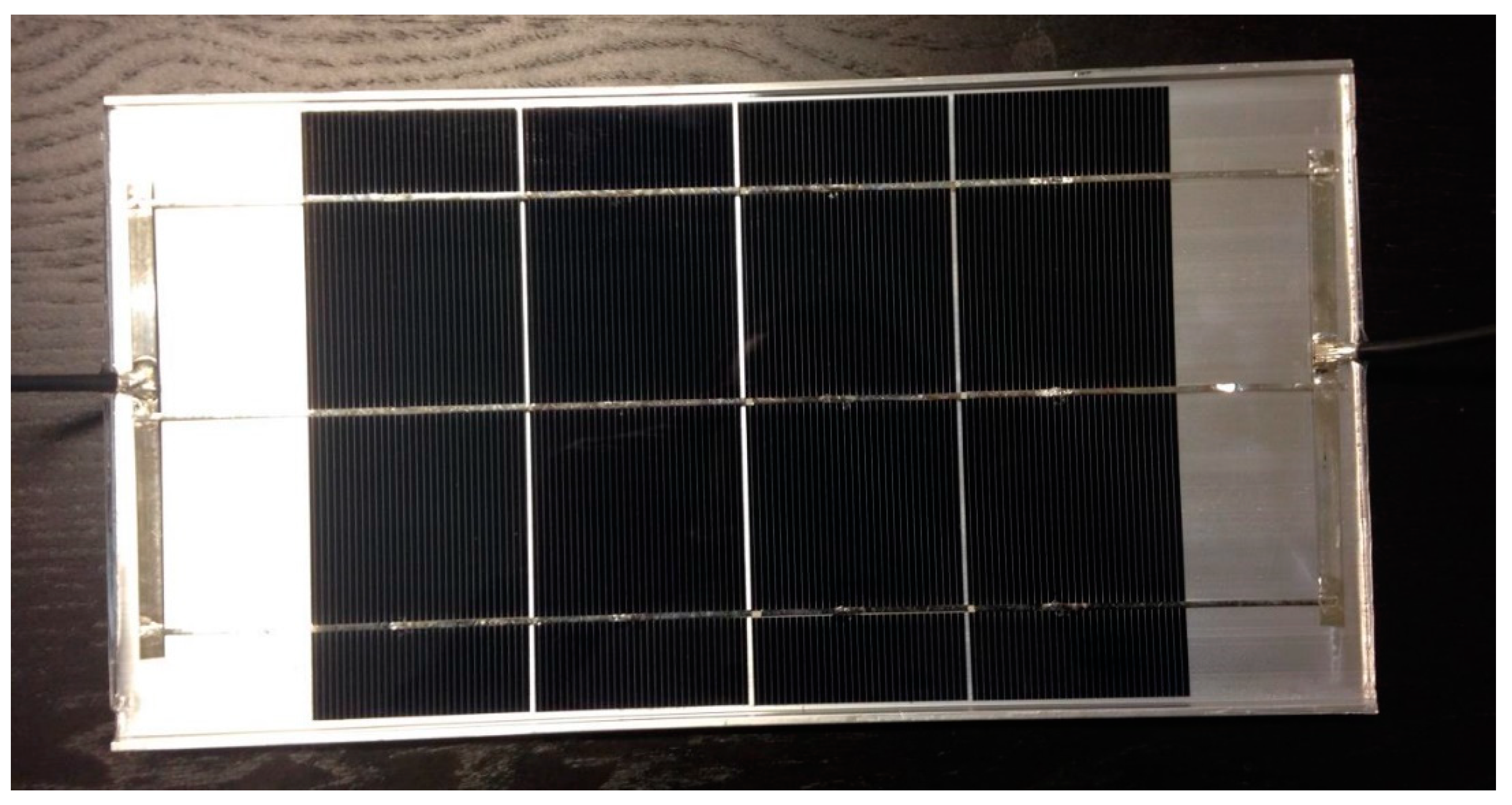
Appendix A presents a picture of each of this receivers for completeness.
The eight receivers were identical with the exception of the six parameters that were varied: Cell size, cell gap, number of cells, type of soldering, type of silicon used and existence of a strain relief.
Four of this six parameters are further explained below:
  • Two cell sizes were used: 1/3 (52 × 148 mm) and 1/6 (28 × 148 mm);
  • The cell gap is the space between the cells. The word “No” means that the small standard cell gap of 0.5mm was utilized, while “Yes” means a longer gap (triple of the standard gap);
  • The strain relief is an exaggerated “s” shape bent in the tabbing strip between each cell. The goal is that this shape absorbs the thermally-induced mechanical stress, instead of the cells.
  • As mentioned earlier the silicone is applied in two layers. An initial bottom layer that is placed on the aluminium receiver before the cells and a top layer that is placed at the same time as the solar cells, after the initial bottom layer of silicone has already solidified. Two types of silicone were used, as described in Section 2.1.

2.4. Test Method and Equipment

The testing procedure consisted of submitting each receiver to eight rounds of gradually increasing temperatures inside an oven for a duration of one hour. In the first round the receiver temperature was raised from room temperature to 60 °C, and in the next rounds from room temperature to 80 °C, 100 °C, 130 °C, 150 °C, 180 °C, 200 °C, and finally to 220 °C. This process was repeated in exactly the same manner for all receivers. The Table 2 below describes the heating rounds:
It is important to point out that the collectors stagnation temperature is 180 °C. Nevertheless, the tests at 200 °C and 220 °C give interesting results in order to determine a safety margin.
Before and after each thermal cycle round, the following parameters were recorded:
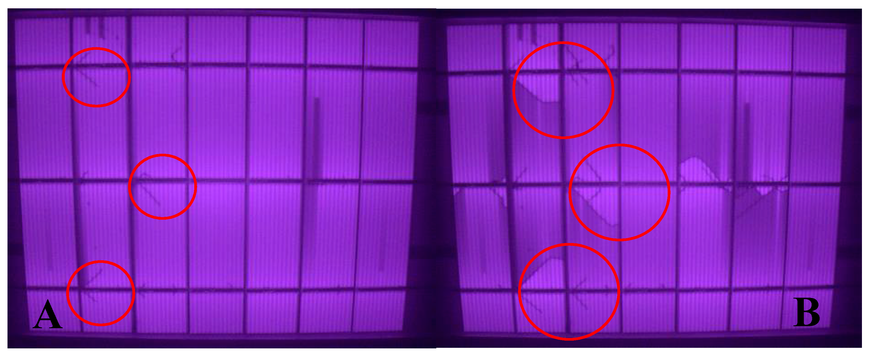
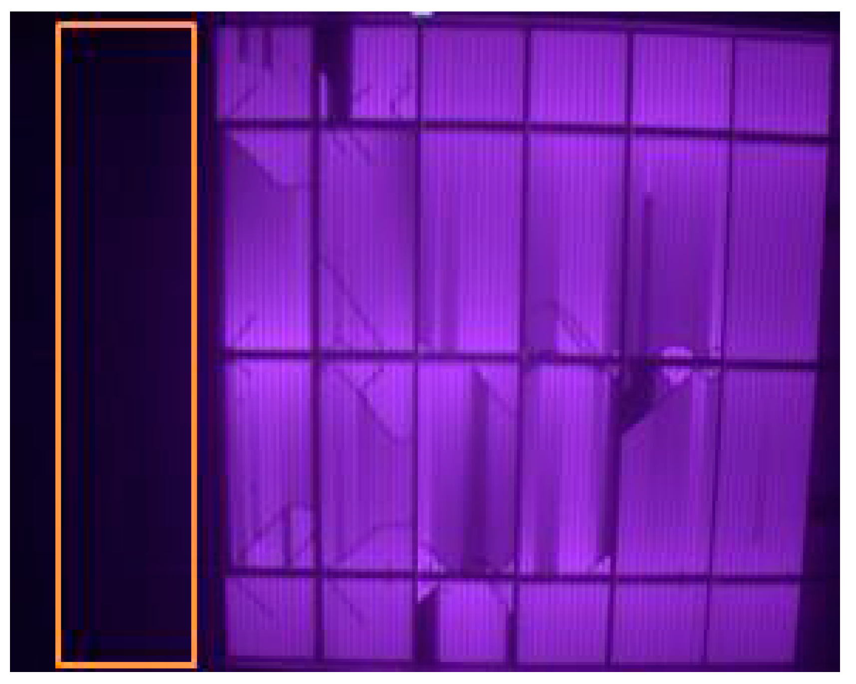
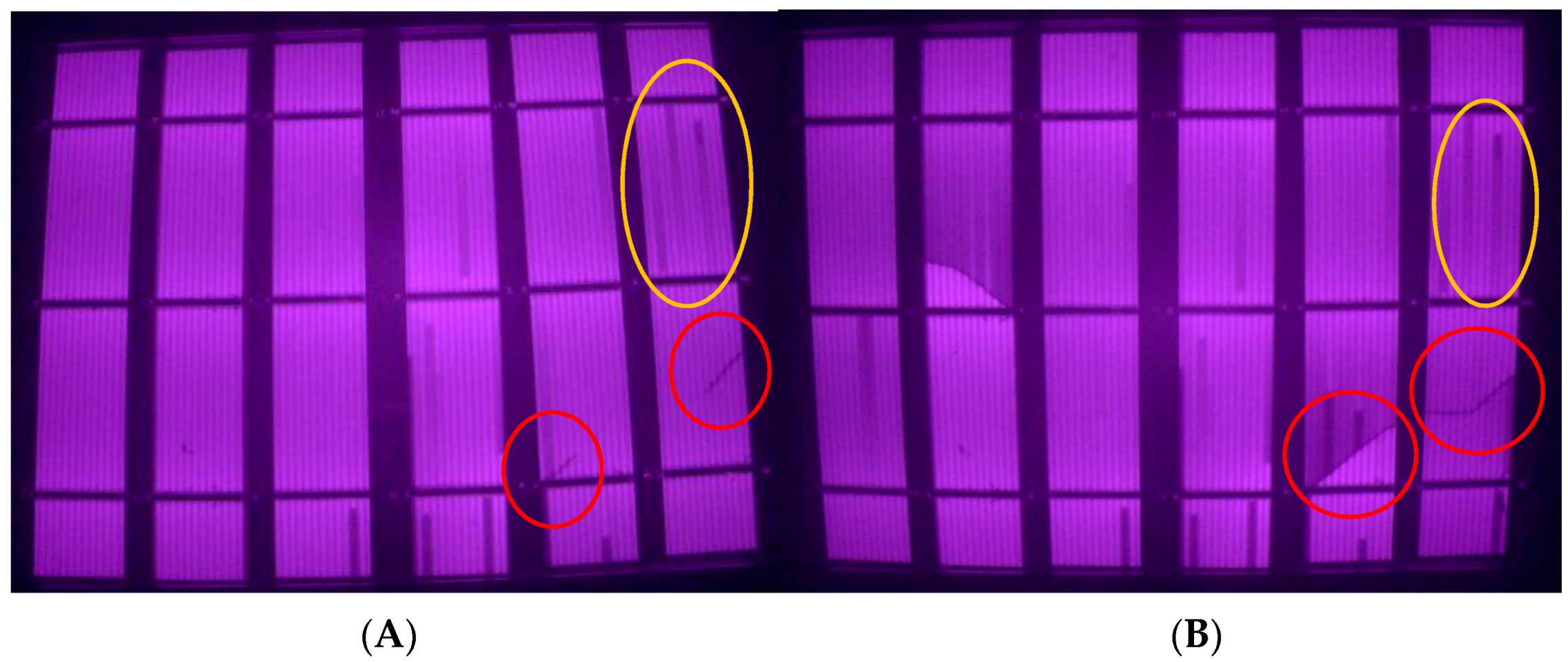
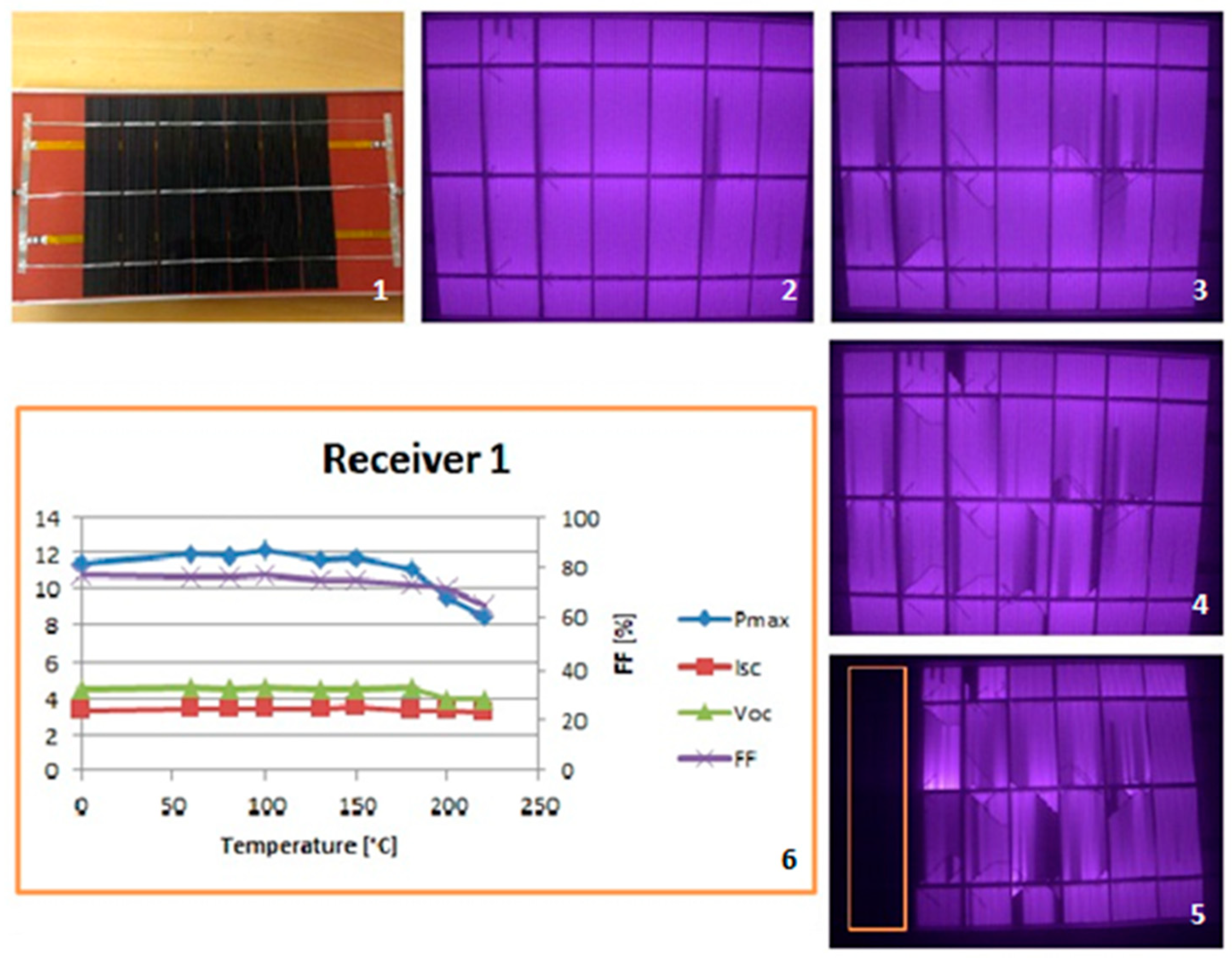
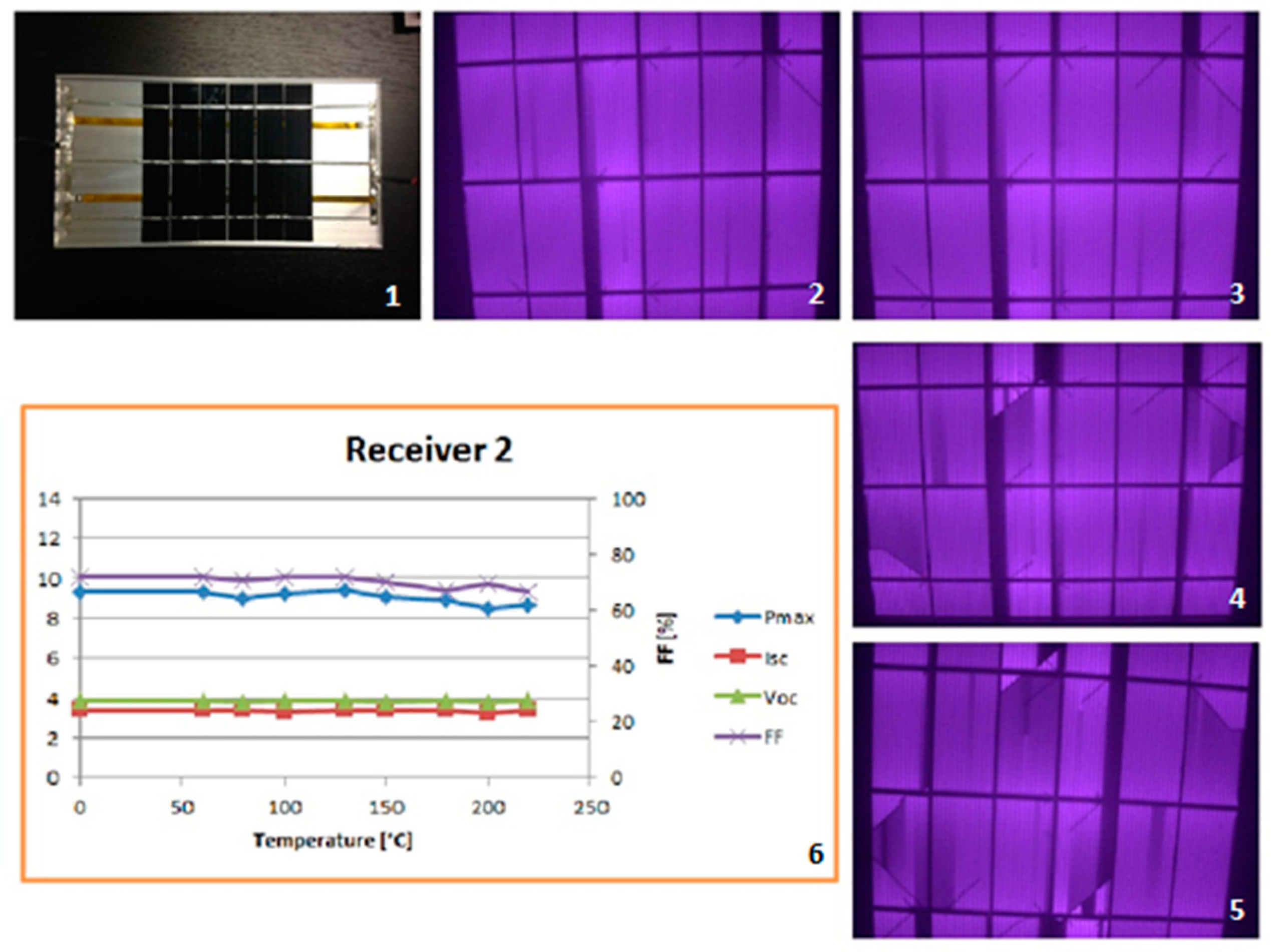
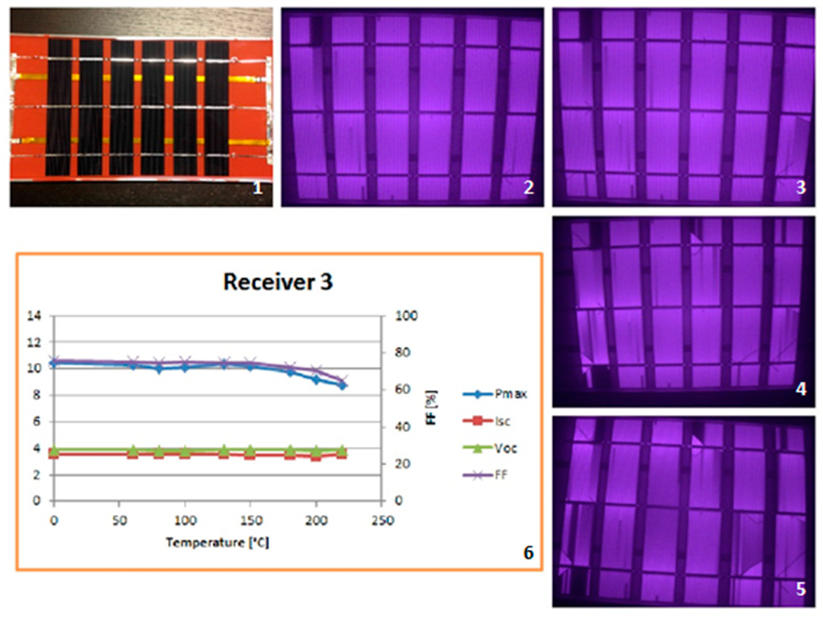
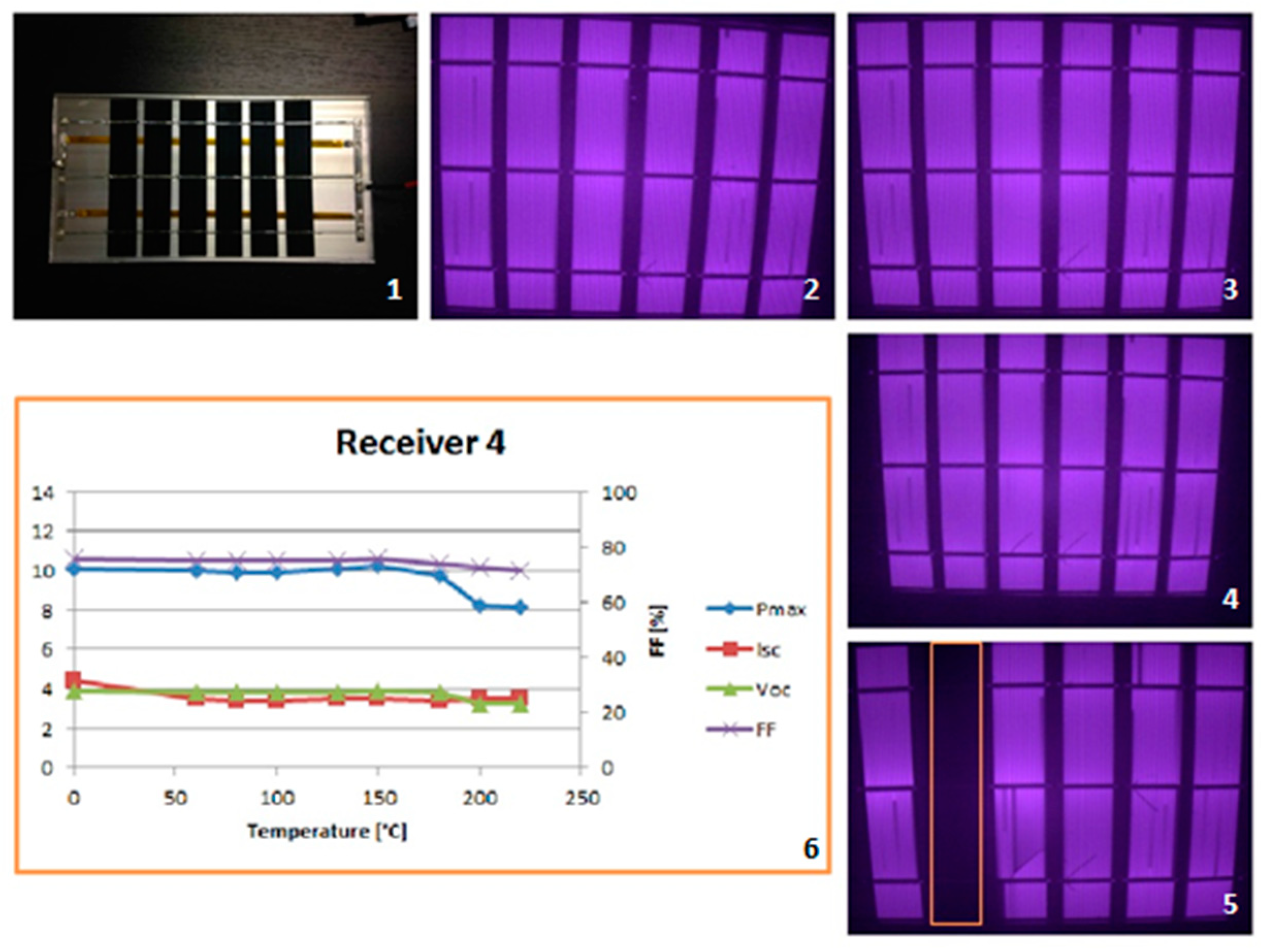
  • Electroluminescence Test: IR photograph of the cells on the receiver was made using a Digital Rebel XTi Black Canon Camera without an IR filter. The system features an image size of (3888 × 2592) in RAW format with 10 megapixels. The test was done in a completely dark chamber. Cells were in forward bias with a current close to 4A. This test allowed the team to spot microcracks that would otherwise not be visible to the naked eye.
  • Diode Function test, which yielded a response of working or not working.
  • Visual Inspection, which consisted in a simple visual check to the overall condition of the cells, discoloration of the silicone or any other potential issue.
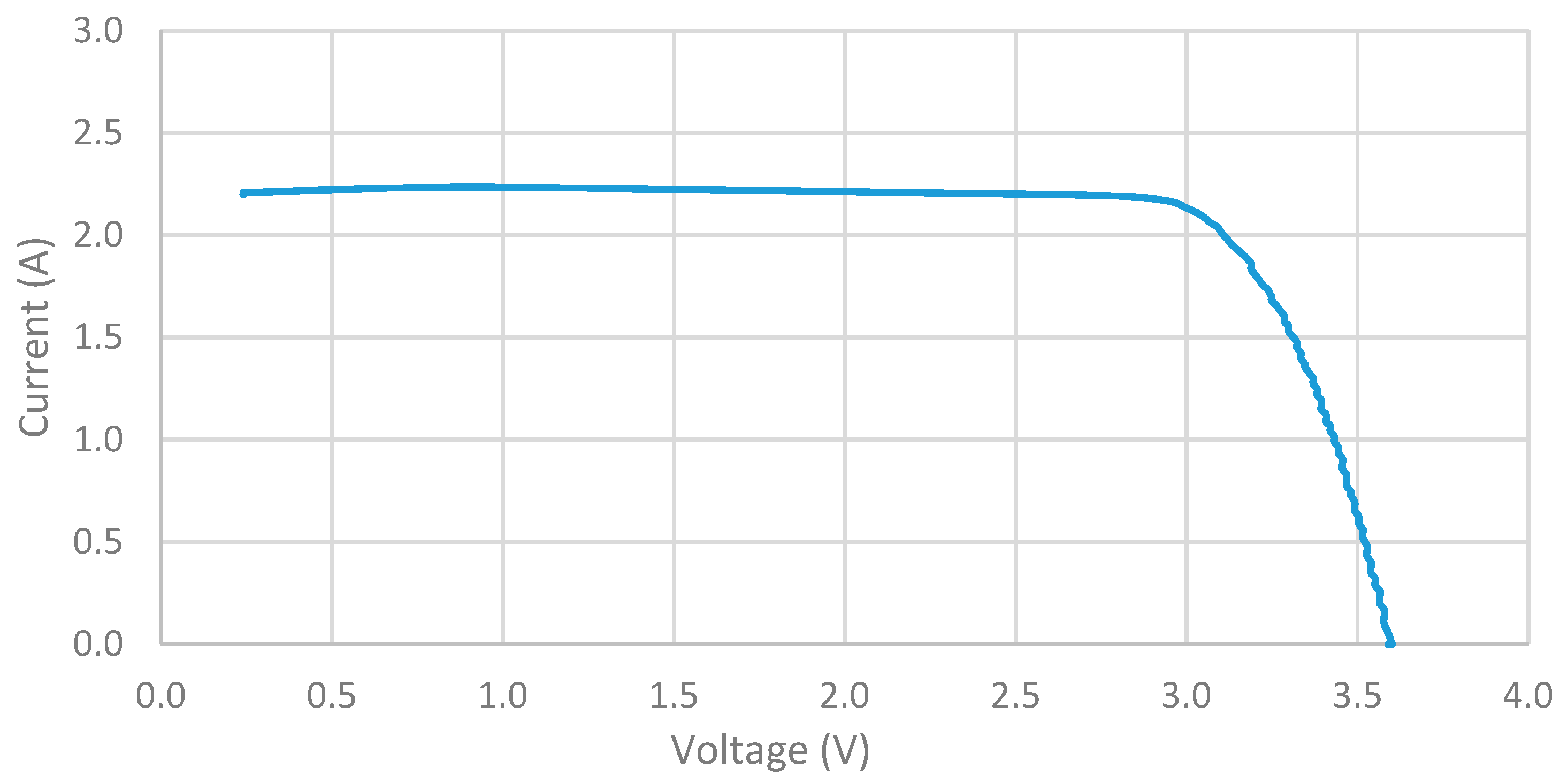
  • IV Curve test with an IV tracer in a solar simulator. The following parameters were measured: Short circuit current (Isc), open circuit voltage (Voc), current at maximum power point (Imp), voltage at maximum power point (Vmp), maximum power point (Pmax) and fill factor (FF).
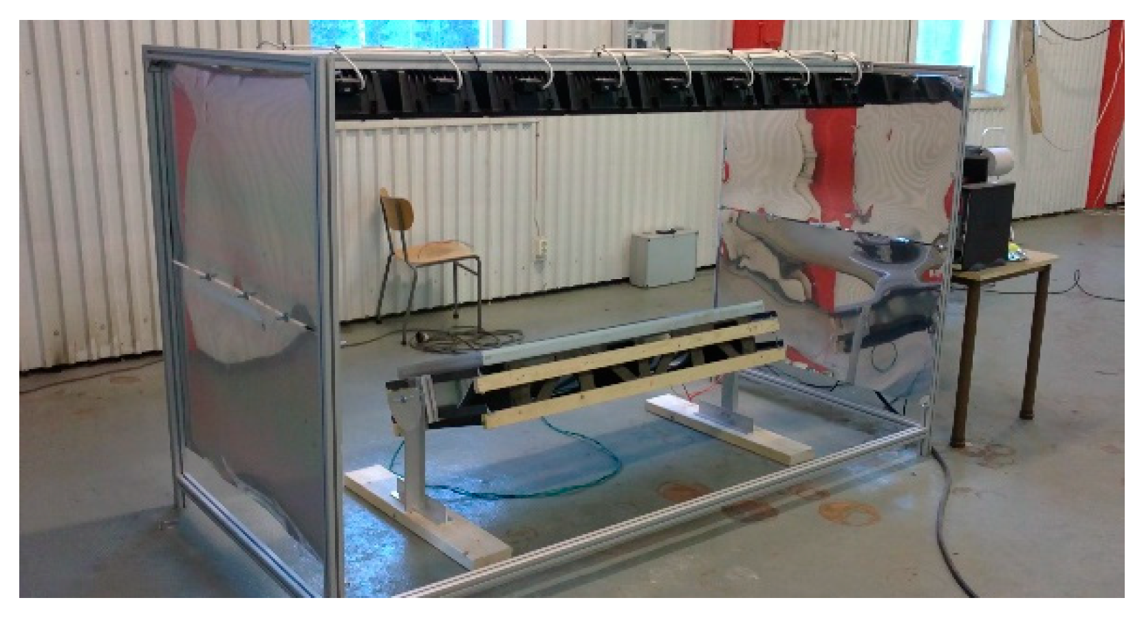
The indoor solar simulator shown in Figure 4 was utilized for the IV-curves. It consists of two rows of 8 halogen light bulbs each with 1000 W of power. As in many solar simulators, the light distribution and spectrum can be a draw-back, since it is understandably hard to simulate the energy coming from the sun, a stellar object that is a nearly perfect sphere of hot plasma with a diameter of 1.39 million kilometers and a mass that is about 330,000 times that of Earth. Regardless, for the objective of the comparative measurements between receivers, this solar simulator is well suited.
An important consideration about these eight prototype receivers is that the cells were soldered manually which means that some microcracks arise from the production process that would not occur in automatic cell soldering production. This means that the baseline round was a fundamental check to account for damages that were not caused by the stagnation.

3. Results and Discussion

3.1. Calculation of the Stagnation Temperature for the C-PVT Prototype

The thermal efficiency curve of the prototype C-PVT can be calculated by using the simplified Equation (1):
ηThermal = η0 + a × (Tmed − Tamb),
where η0 is the optical efficiency of the prototype collector when electricity is being extracted, a is the heat loss factor, Tmed is the average temperature of the collector and Tamb is the ambient temperature.
In this manner, and using the collector data detailed in Section 2.1, the resulting efficiency curve is shown in Figure 5:
Based on the ISO 9806 [5,6] and the summary report on stagnation temperature [7], the stagnation temperature of the prototype collector is given by the no flow temperature reached by the collector (under a radiation of 1000 W/m2 and a wind speed below 1 m/s) summed to an ambient temperature of 30 °C. This gives a stagnation temperature of 150 + 30 = 180 °C.

3.2. Evaluation of Microcracks under Electroluminescence

Figure 6a shows the baseline scenario (ambient temperature) of receiver 1 and the red circles highlight small microcracks that are caused by manufacturing while Figure 6b shows how these initial microcracks have expand in size after being heated in successive rounds, until the round with a temperature of 130 °C. Additionally, Figure 6b shows that new microcracks have appeared, although the majority of the cracks come from the expansion of initially existing cracks.
Figure 7 shows the status of receiver 1 after the round 200 °C. Adding to the microcracks, there is also a completely black cell highlighted in orange, which means that there is a short circuit between top and bottom of the cell, potentially caused by the top and bottom ribbon coming into contact through the broken cell.
Figure 8 shows receiver 5 at the baseline and at 200 °C. The red circles show again microcracks caused by the manual production process and their expansion when heated up, although in this receiver the cracks take longer to expand. The yellow circle shows the small flaws in the cell, potentially caused during the production process of the cell or the cell wafer. These flaws seem to influence the appearance of new microcracks.
It was the author’s expectation that receiver 1 would be the receiver design least capable to withstand stagnation, while receiver 5 was expected to be one of the most successful designs, which the above images confirm.
This way, three main types of issues were identified:
-
Microcracks caused by manual soldering; (Figure 6),
-
Short circuit in one cell; (Figure 7)
-
Flaws from cell production; (Figure 8)

3.3. Summary of the Thermal Stress Test Results on All Prototype Receivers

Eight receivers were built and stress tested at eight temperatures. The following eight figures show an image of the receivers, four EL test images and a graph with the parameters of the tested receiver. For all receivers, the visual inspection did not provide additional information. In Appendix B, it is also possible to see an example of an IV curve.
The first receiver tested had the same design characteristics as the collectors of the installation shown in Figure 3 and, as such, was expected to show a substantial amount of microcracks.
This way, as expected, after round 5 (exposure to 150 °C which is number 3 in the Figure 9), the image from the EL test showed that the string had dark areas and a large number of microcracks, which led to a power decreases shown in graph. Raising the temperature in following heating rounds has significantly increased the amount of dark areas and microcracks. In the last round, one cell became completely black, which is most likely caused by a short circuit between the top and bottom of the cell. The reason for the short circuit has not been determined but a likely explanation is that the solder on the top ribbon melted (or simply became in contact) through a crack and reached the bottom ribbon.
The only difference between the first receiver and the second is the bottom silicone layer. In receiver 2, transparent silicone was used on both layers. From the five rounds of EL tests shown in Figure 10, it is possible to see a large increase in microcracks after round 6 (180 °C). Despite this, the IV curve basic parameters remain more or less constant throughout the eight rounds with only a minor power decrease. The number of microcracks in receiver 1 is higher than in receiver 2 for all temperatures, despite the baseline test (image 2 of Figure 10) having a slight higher number of microcracks.
The main goal of building receivers 3 and 4 was to evaluate the impact of the thermal expansion of the ribbon on the cell. This way, a strain relief bend was inserted before and after each cell. In order to isolate the impact of the different types of silicones two receivers were made with this type of strain relief ribbon: One with red silicone (receiver 3) and another with transparent silicone (receiver 4). The results from receiver 3 can be seen in Figure 11 and from receiver 4 in Figure 12.
The EL tests in Figure 11 show that in a receiver with red silicone, even with the strain relief between the cells, a large number of microcracks appear when exposed to high temperatures (180 °C). Compared with receiver 1, receiver 3 exhibits a smaller power drop, albeit still displaying a significant power drop in the last 2 rounds.
The cells of receiver 4, shown in Figure 12, have no significant damage along the 8 rounds, representing a clear improvement from the results obtained with receiver 2. However, receiver 4 showed one black cell in the last round likely due to the same reason as in the receiver 1. The same black cell, which appeared in round 7 (200 °C), is also responsible for the sharp 15% drop. Excluding that effect, the power remains considerably constant.
Since our research group did not have, at the time of these tests, access to an expensive automatic cell soldering machine, it was also important to investigate the impact of different manual soldering techniques. To this effect, receivers 5 and 6 have been made with point soldering instead of continuous soldering, like all previous receiver. Point soldering is far easier to accomplish with manual soldering and less likely to create microcracks during the production process. Receiver 5 was done with two point soldering and strain relief, while receiver 6 had no strain relief and only one point soldering.
In the graph of Figure 13, it is visible that the Pmax of receiver 5 has one initial decrease at 50 °C. This drop is due to the two broken cells shown in image three. If this effect is excluded, the Pmax remains relatively stable. It is interesting to note that only at 220 °C one extra microcrack appears. The one point soldering has much smaller electrical contact between the busbar and the cell than the line soldering but this shows no consequences in term of measurement power output, due to the fact that the current through the cells is low.
In Figure 14, the Pmax of receiver 6 also remains fairly stable until one of the cell becomes dark at 200 °C (round 7) which seems to indicate that there are no large differences between one and two point soldering when combined with a strain relief. One microcrack appears at 180 °C and another appears at 220 °C.
Receivers 7 and 8 were made to evaluate the impact of temperature in larger cells (148 × 52 mm). Receiver 7 was made with a larger gap than usual between the cells, with line soldering and with strain relief between all cells, while receiver 8 was made without strain relief, with point soldering and with a standard gap between cells.
Despite having more precautions against stagnation, receiver 7 shows more cell breakage than receiver 8 at any temperature. This seems to point that on large cells the effect of having large gaps with strain relief is less important than the type of soldering.
Strangely, the decrease in power is more pronounced in receiver 8 than in receiver 7, as can be seen in Figure 15 and Figure 16. However, it must be noted that receiver 7 starts from a lower baseline scenario since it shows some microcracks from the beginning. From all the testing accomplished, it also seems safe to state that existing microcracks expand at faster rate than new microcracks are created.
Figure 17 compares the decrease in Pmax of the different receivers at different temperatures rounds with and without the strain relief. Receiver 2 shows the most stable Pmax across all temperatures. Receiver 5 is also fairly stable if the handling problem on round 1 is excluded. Receiver 1 shows an increase of power that is difficult to explain and is assumed to have been a human measurement error, potentially combined with the small variation in the power provided by the solar simulation. Overall, receivers with red silicone have the highest power decrease, when external factors are excluded. The existence of gaps seems to reduce the number of microcracks. No prototype receiver loses more than 30% of its initial power, despite the large cell breakage shown by some of the prototype receivers in the EL imaging results.

4. Conclusions

Eight receivers have been built and were successfully tested to assess the impact of reaching high temperatures in the performance and cell structural integrity.
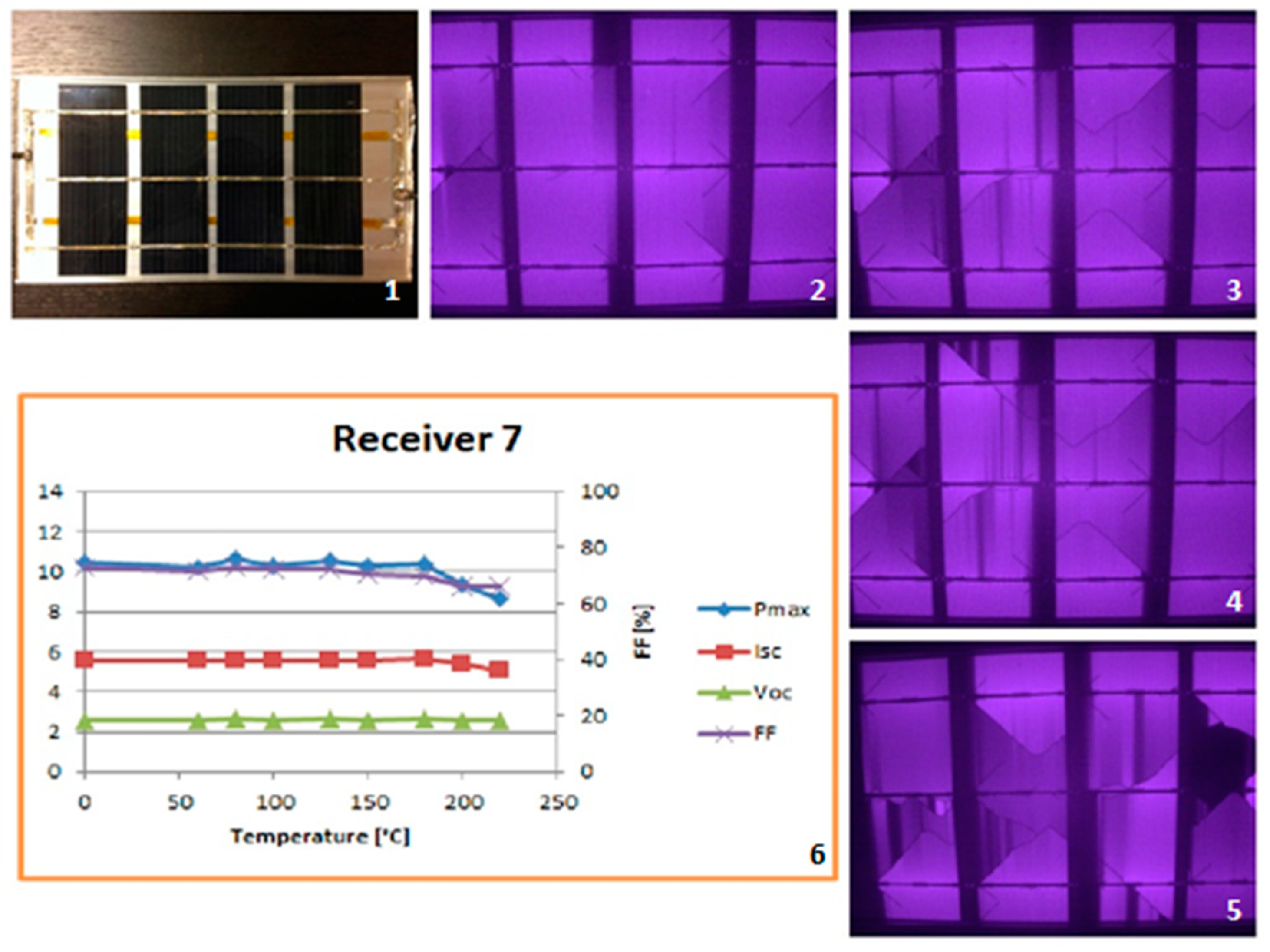
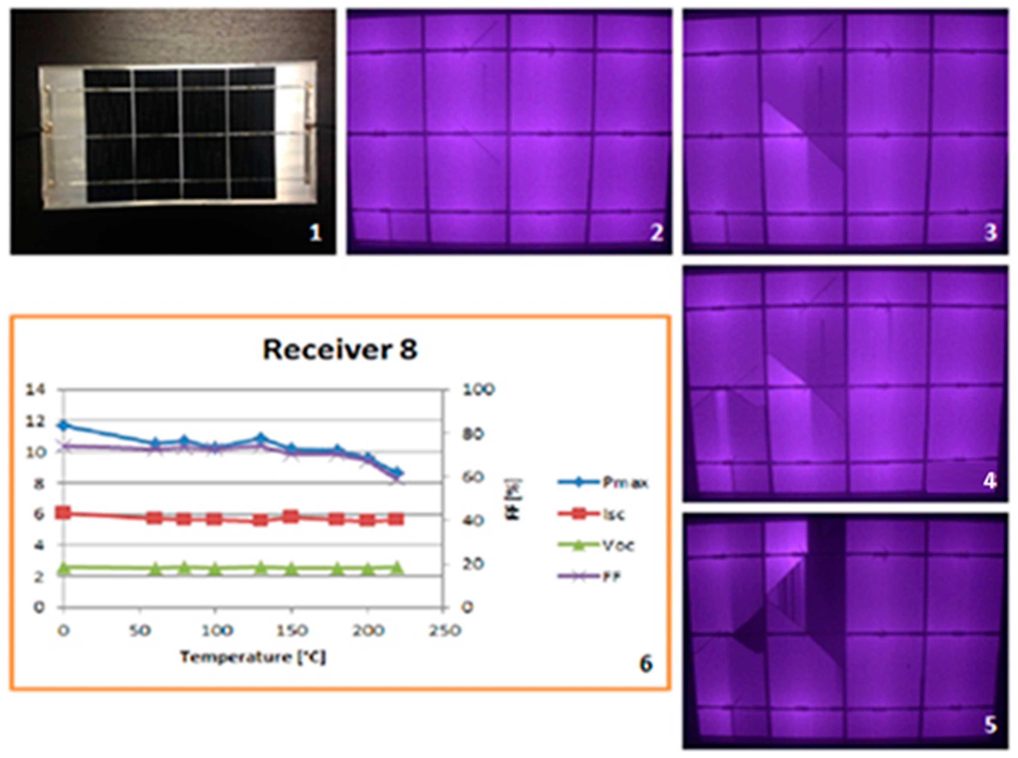
The EL testing allowed identifying two main types of problems in the solar cells which are represented by black areas in the cell EL image. One is the irregularly shaped areas which are due to microcracks, and the other is regular rectangular areas which are due to broken finger contacts on the front of the cell. It was also noted that the majority of the microcracks were initiated at the soldering points, which is understood to happen due to the different expansion coefficients between the copper ribbon and the silicon solar cell. A third problem was also detected which is due to flaws in production process at either wafer or cell production. These three issues are highlighted in the images show in Section 3.2.
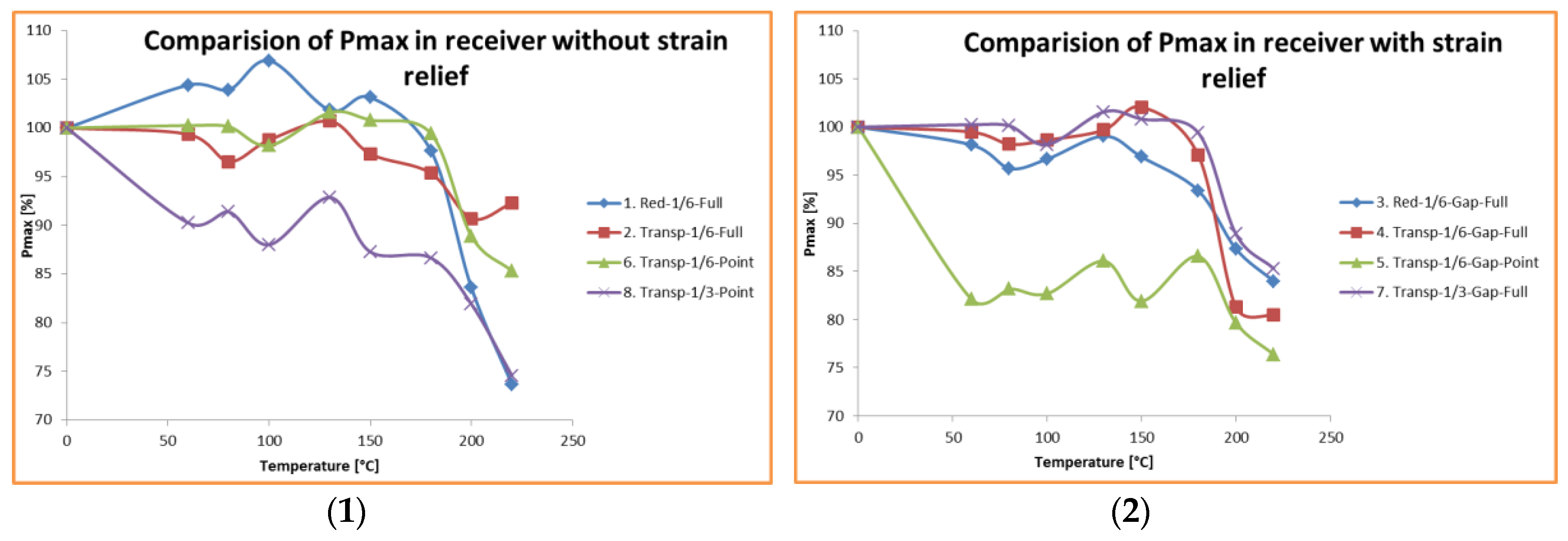
From the figures shown in the results section, it is clear that receivers built with transparent silicone show far less cracks and power degradation after being exposed to stagnation temperatures. This is understood to be due to two main reasons: (1) the transparent silicone is not so stiff as the red silicone and thus further absorbs the mechanical stress of thermal expansion in the aluminium receiver; (2) the red silicone due to its lower viscosity is normally made in a thinner layer which further penalizes its ability to absorb mechanical stress.
No prototype test receiver lost more than 30% of its initial power, despite the large cell breakage shown in the EL imaging of some receivers. After eight rounds of testing in eight receivers with different designs, it was possible to conclude that the diodes were working perfectly at all temperatures, despite the diode specifications stated a maximum junction temperature of only 200 °C.
Larger cells are more prone to develop microcracks due to thermally induced stresses. From the tests that have been made, point soldering seems to lead to a reduction in the number of microcracks and black areas, especially in receivers with larger cells (148 × 52mm instead of 148 × 26 mm). However, the impact of microcracks in the Pmax of receivers with point soldering is also larger due to the smaller contact area between the ribbon and the cell.
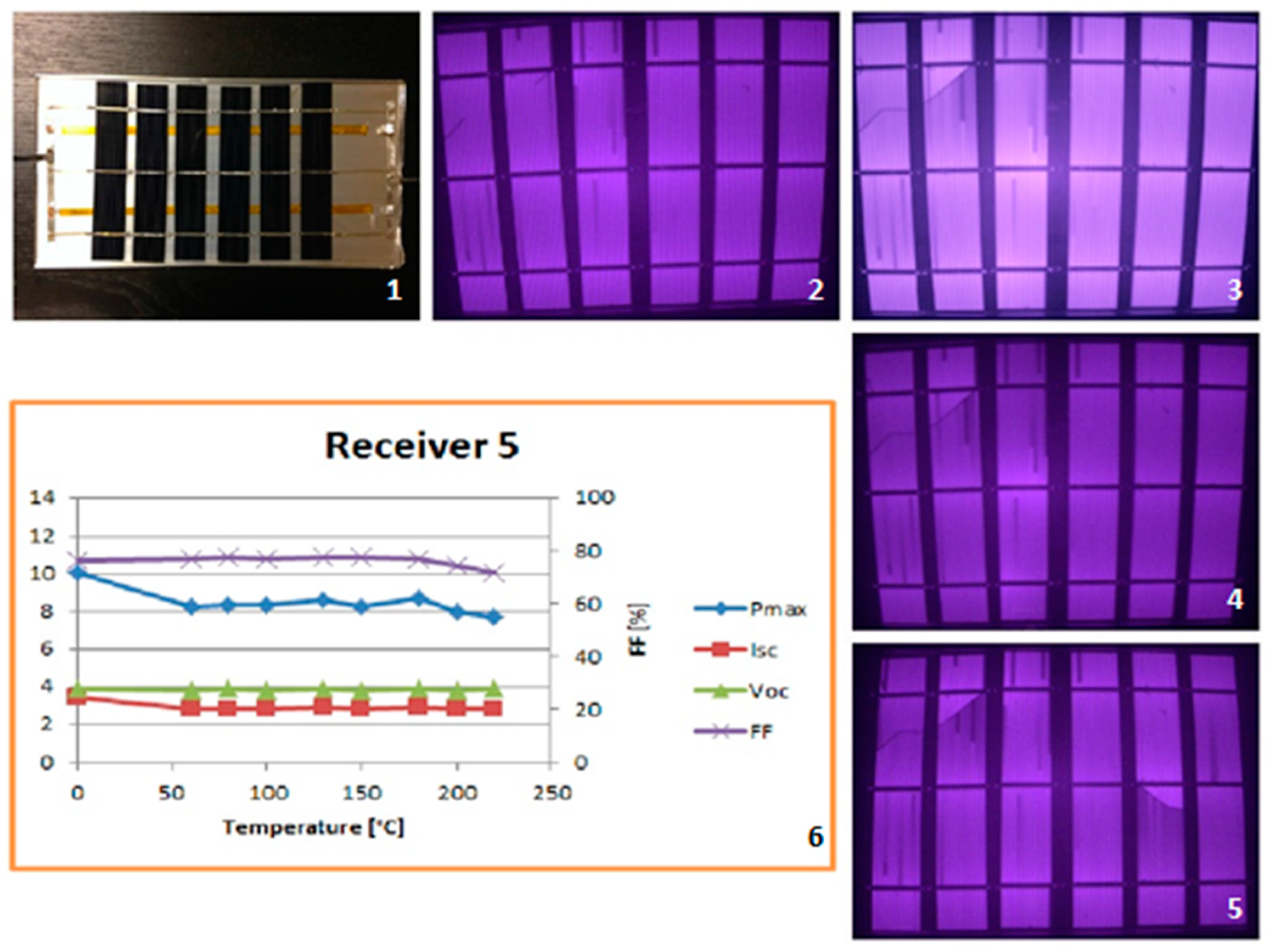
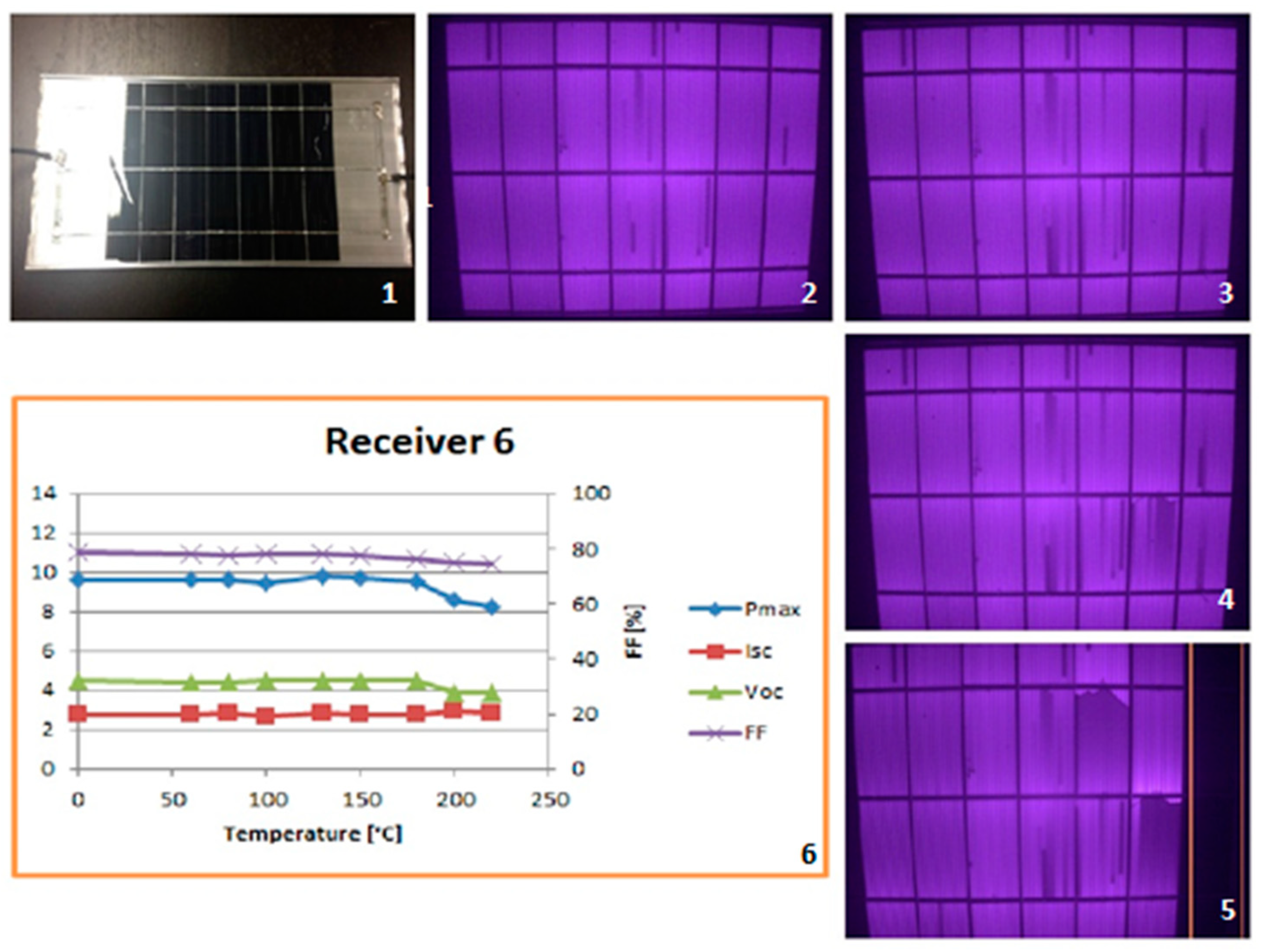
From the EL images, the receiver presenting the lowest amount of microcracks after round 8 (at 220 °C) is receiver 5. This receiver was made with point soldering and a strain relief between each cell. Receiver 4 and receiver 6 also exhibit low amounts of microcracks but both have a full black cell, possibly caused by the top and bottom ribbon becoming in contact through a cell crack or a melted ribbon. Receiver 2 shows the steadiest Pmax across all temperatures. Receiver 5 is also fairly stable, if the human handling error is excluded.
This study also allows to conclude that existing microcracks tend to grow in size into larger cracks. The EL imaging taken during our experiment leads us to conclude that it is far easier for existing cracks to expand than for new cracks to appear.
A limitation of this work was the absence of a fully automatic tabbing machine. Since this is expensive equipment that was not available at the time of these experiments, our team was forced to use manual soldering. However, by setting a baseline scenario for comparison, this limitation was sufficiently addressed.
It is important to point out that the thickness of the bottom silicone layer is of the upmost importance in reducing the transference of thermally induced stress to the cells. The impact of the variations in the thickness of silicone in the thermal stress suffered by the cells has not been evaluated in this paper and should be addressed in a future study since it is a very relevant aspect for cell survival of stagnation.

Funding

This research was funded by Eureka Eurostars, Project E10625—Solar CPC PVT Production, and the company Solarus Sunpower.

Acknowledgments

The author would like to acknowledge all the technical work carried out by Linkesh Diwan, Mafalda Henriques, Silvio Bastos and Olle Olsson during the experiments. Additionally, the author would like to acknowledge the advisory support given by Björn Karlsson.

Conflicts of Interest

The funders had no role in the design of the study; in the collection, analyses, or interpretation of data; in the writing of the manuscript, or in the decision to publish the results.

Appendix A

Appendix A (Figure A1, Figure A2, Figure A3, Figure A4, Figure A5, Figure A6, Figure A7 and Figure A8) shows an image of all receivers for easier comprehension of the tested designs.
Figure A1. Receiver 1 has seven 1/6 cells with a standard cell gap, line soldering, red and transparent silicon and no strain relief.
Energies 12 02967 g0a1
Figure A2. Receiver 2 has six 1/6 cells with a standard cell gap, line soldering, transparent silicon only and no strain relief.
Energies 12 02967 g0a2
Figure A3. Receiver 3 has six 1/6 cells with a larger cell gap, line soldering, red and transparent silicon and strain relief.
Energies 12 02967 g0a3
Figure A4. Receiver 4 has six 1/6 cells with a larger cell gap, line soldering, transparent silicon only and strain relief.
Energies 12 02967 g0a4
Figure A5. Receiver 5 has six 1/6 cells with a larger cell gap, line soldering, transparent silicon only and strain relief.
Energies 12 02967 g0a5
Figure A6. Receiver 6 has seven 1/6 cells with a standard cell gap, one point soldering, transparent silicon only and no strain relief.
Energies 12 02967 g0a6
Figure A7. Receiver 7 has four 1/3 cells with a large cell gap, line point soldering, transparent silicon only and strain relief.
Energies 12 02967 g0a7
Figure A8. Receiver 8 has four 1/3 cells with a standard cell gap, one point soldering, transparent silicon only and no strain relief.
Energies 12 02967 g0a8

Appendix B

Appendix B (Figure A9) shows an example of an IV curve conducted in receiver 5 after the 220 °C round of heating.
Figure A9. IV curve for receiver 5 after being exposed to all testing rounds
Energies 12 02967 g0a9

References

  1. Giovinazzo, C.; Bonfiglio, L.; Gomes, J.; Karlsson, B. Ray, Tracing Modelling of an Asymmetric Concentrating PVT. In Proceedings of the Eurosun Proceeding, Aix-les-Bains, France, 16 September 2014. [Google Scholar]
  2. Bernardo, R.; Davidsson, H.; Gentile, N.; Gomes, J.; Gruffman, C.; Chea, L.; Mumba, C.; Karlsson, B. Measurements of the Electrical Incidence Angle Modifiers of an Asymmetrical Photovoltaic/Thermal Compound Parabolic Concentrating-Collector. Engineering 2012, 5, 37–43. [Google Scholar]
  3. Gomes, J.; Diwan, L.; Bernardo, R.; Karlsson, B. Minimizing the Impact of Shading in a Stationary Asymmetric Concentrating PVT Collector. Energy Procedia 2014, 57, 2176–2185. [Google Scholar]
  4. Cabral, D.; Karlsson, B.O. Electrical and thermal performance evaluation of symmetric truncated C-PVT trough solar collectors with vertical bifacial receivers. Sol. Energy 2018, 174, 683–690. [Google Scholar] [CrossRef]
  5. ISO 9806. Solar Energy-Solar Thermal Collectors–Test Methods. 2013. Available online: https://www.iso.org/standard/59879.html (accessed on 15 February 2019).
  6. ISO 9806. Solar Energy-Solar Thermal Collectors–Test Methods. 2017. Available online: https://www.iso.org/obp/ui/#iso:std:iso:9806:ed-2:v1:en (accessed on 15 February 2019).
  7. Helminger, F. Summary report on Stagnation temperature. Austrian Institute of Technology, Quality assurance in solar thermal heating and cooling technology: Keeping track with recent and upcoming developments (QAIST). 2012. [Google Scholar]
  8. Menéndez, O.; Guamán, R.; Pérez, M.; Cheein, F. Photovoltaic Modules Diagnosis Using Artificial Vision Techniques for Artifact Minimization. Energies 2018, 11, 1688. [Google Scholar] [CrossRef]
  9. Wang, Y.; Itako, K.; Kudoh, T.; Koh, K.; Ge, Q. Voltage-Based Hot-Spot Detection Method for Photovoltaic String Using a Projector. Energies 2017, 10, 230. [Google Scholar] [CrossRef]
  10. Eder, G.; Voronko, Y.; Hirschl, C.; Ebner, R.; Újvári, G.; Mühleisen, W. Non-Destructive Failure Detection and Visualization of Artificially and Naturally Aged PV Modules. Energies 2018, 11, 1053. [Google Scholar] [CrossRef]
  11. Gosumbonggot, J.; Fujita, G. Global Maximum Power Point Tracking under Shading Condition and Hotspot Detection Algorithms for Photovoltaic Systems. Energies 2019, 12, 882. [Google Scholar] [CrossRef]
  12. Filik, U.; Filik, T.; Gerek, Ö. A Hysteresis Model for Fixed and Sun Tracking Solar PV Power Generation Systems. Energies 2018, 11, 603. [Google Scholar] [CrossRef]
  13. Charalambousa, P.G.; Maidmenta, G.G.; Kalogiroub, S.A.; Yiakoumettia, K. Photovoltaic thermal (PV/T) collectors: A review. Appl. Therm. Eng. 2007, 27, 275–286. [Google Scholar] [CrossRef] [Green Version]
  14. Widyolar, B.K.; Abdelhamida, M.; Jianga, L.; Winston, R.; Yablonovitch, E.; Scranton, G.; Cygan, D.; Abbasic, H.; Kozlovc, A. Design, simulation and experimental characterization of a novel parabolic trough hybrid solar photovoltaic/thermal (PV/T) collector. Renew. Energy 2017, 101, 1379–1389. [Google Scholar] [CrossRef] [Green Version]
  15. Khatri, R.; Agarwa, S.; Saha, I.; Singh, S.; Kumar, B. Study on long term reliability of photo-voltaic modules and analysis of power degradation using accelerated aging tests and electroluminescence technique. Energy Procedia 2011, 8, 396–401. [Google Scholar] [CrossRef] [Green Version]
  16. Chaturvedi, P.; Hoex, B.; Walsh, T.M. Broken metal fingers in silicon wafer solar cells and PV modules. Sol. Energy Mater. Sol. Cells 2012, 108, 78–81. [Google Scholar] [CrossRef]
  17. Gomes, J.; Bastos, S.; Henriques, M.; Diwan, L.; Olsson, O. Evaluation of the Impact of Stagnation Temperatures in Different Prototypes of Low Concentration PVT Solar Panels. In Proceedings of the ISES Conference Proceedings, Solar World Conference, Daegu, Korea, 8–12 November 2015. [Google Scholar]
  18. Solarus Website. Available online: www.solarus.com (accessed on 4 December 2018).
  19. Adsten, M.; Helgesson, A.; Karlsson, B. Evaluation of CPC-collector designs for stand-alone, roof or wall installation. Sol. Energy 2005, 79, 638–647. [Google Scholar] [CrossRef]
  20. Rönnelid, M.; Perers, B.; Karlsson, B. Construction and testing of a large-area CPC-collector and comparison with a flat plate collector. Sol. Energy 1996, 57, 177–184. [Google Scholar] [CrossRef]
Figure 1. Top view of the C-PVT collector. The water connections are marked in blue and the electrical connections in red [2].
Energies 12 02967 g001
Figure 2. Prototype C-PVT collector.
Energies 12 02967 g002
Figure 3. Prototype installation consisting of eight C-PVT collectors (closer) and six concentrating thermal collectors (farther).
Energies 12 02967 g003
Figure 4. The solar simulator for the indoor measurements.
Energies 12 02967 g004
Figure 5. Thermal efficiency curve of the prototype collector.
Energies 12 02967 g005
Figure 6. EL test of receiver 1: (A) Baseline (ambient temperature); (B) After the round at 130 °C.
Energies 12 02967 g006
Figure 7. EL test of receiver 1 after the round at 200 °C.
Energies 12 02967 g007
Figure 8. EL test of receiver 5. (A) Baseline (ambient temperature); (B) After the round at 200 °C.
Energies 12 02967 g008
Figure 9. (1) Receiver 1; (2) Baseline Round; (3) Round 5 (150 °C); (4) Round 6 (180 °C); (5) Round 8 (220 °C); (6) Parameters of the IV curve at different temperatures (Isc, Voc and Pmax shown in the left Y axis and FF in the right Y axis).
Energies 12 02967 g009
Figure 10. (1) Receiver 2; (2) Baseline Round; (3) Round 5 (150 °C); (4) Round 6 (180 °C); (5) Round 8 (220 °C); (6) Parameters of the IV curve at different temperatures (Isc, Voc and Pmax shown in the left Y axis and FF in the right Y axis).
Energies 12 02967 g010
Figure 11. (1) Receiver 3; (2) Baseline Round; (3) Round 5 (150 °C); (4) Round 6 (180 °C); (5) Round 8 (220 °C); (6) Parameters of the IV curve at different temperatures (Isc, Voc and Pmax shown in the left Y axis and FF in the right Y axis).
Energies 12 02967 g011
Figure 12. (1) Receiver 4; (2) Baseline Round; (3) Round 5 (150 °C); (4) Round 6 (180 °C); (5) Round 8 (220 °C); (6) Parameters of the IV curve at different temperatures (Isc, Voc and Pmax shown in the left Y axis and FF in the right Y axis).
Energies 12 02967 g012
Figure 13. (1) Receiver 5; (2) Baseline Round; (3) Round 5 (150 °C); (4) Round 6 (180 °C); (5) Round 8 (220 °C); (6) Parameters of the IV curve at different temperatures (Isc, Voc and Pmax shown in the left Y axis and FF in the right Y axis).
Energies 12 02967 g013
Figure 14. (1) Receiver 6; (2) Baseline Round; (3) Round 5 (150 °C); (4) Round 6 (180 °C); (5) Round 8 (220 °C); (6) Parameters of the IV curve at different temperatures (Isc, Voc and Pmax shown in the left Y axis and FF in the right Y axis).
Energies 12 02967 g014
Figure 15. (1) Receiver 7; (2) Baseline Round; (3) Round 5 (150 °C); (4) Round 6 (180 °C); (5) Round 8 (220 °C); (6) Parameters of the IV curve at different temperatures (Isc, Voc and Pmax shown in the left Y axis and FF in the right Y axis).
Energies 12 02967 g015
Figure 16. (1) Receiver 8; (2) Baseline Round; (3) Round 5 (150 °C); (4) Round 6 (180 °C); (5) Round 8 (220 °C); (6) Parameters of the IV curve at different temperatures (Isc, Voc and Pmax shown in the left Y axis and FF in the right Y axis).
Energies 12 02967 g016
Figure 17. (1) Comparison of Pmax decrease in receivers with strain relief; (2) Comparison of Pmax decrease in receivers without strain relief.
Energies 12 02967 g017
Table 1. Characteristics of the eight small receivers.
ReceiverCell SizeCell NumberCell GapSolderingSilicone LayersTabbing Strip
Receiver 11/67NoLineRed-TransparentStraight
Receiver 21/66NoLineBoth transparentStraight
Receiver 31/66YesLineRed-TransparentStrain Relief
Receiver 41/66YesLineBoth transparentStrain Relief
Receiver 51/66YesTwo PointsBoth transparentStrain Relief
Receiver 61/67NoOne PointBoth transparentStraight
Receiver 71/34YesLineBoth transparentStrain Relief
Receiver 81/34NoOne PointBoth transparentStraight
Table 2. The heating rounds for the receivers. (Each round consisted of 1 h inside the oven and 3 h of cooling at room temperature).
Baseline (Round 0)Receiver at Room Temperature
Round 160 °C
Round 280 °C
Round 3100 °C
Round 4130 °C
Round 5150 °C
Round 6180 °C
Round 7200 °C
Round 8220 °C

