Gallium-Nitride Semiconductor Technology and Its Practical Design Challenges in Power Electronics Applications: An Overview


Abstract
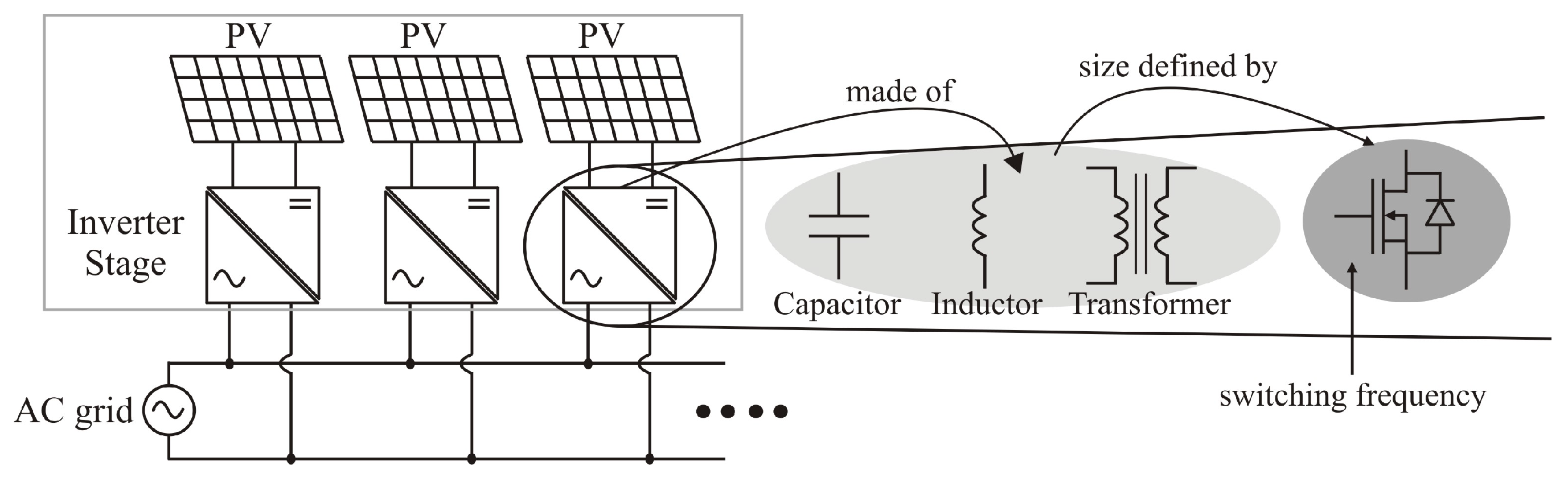
1. Introduction
2. Device Configuration
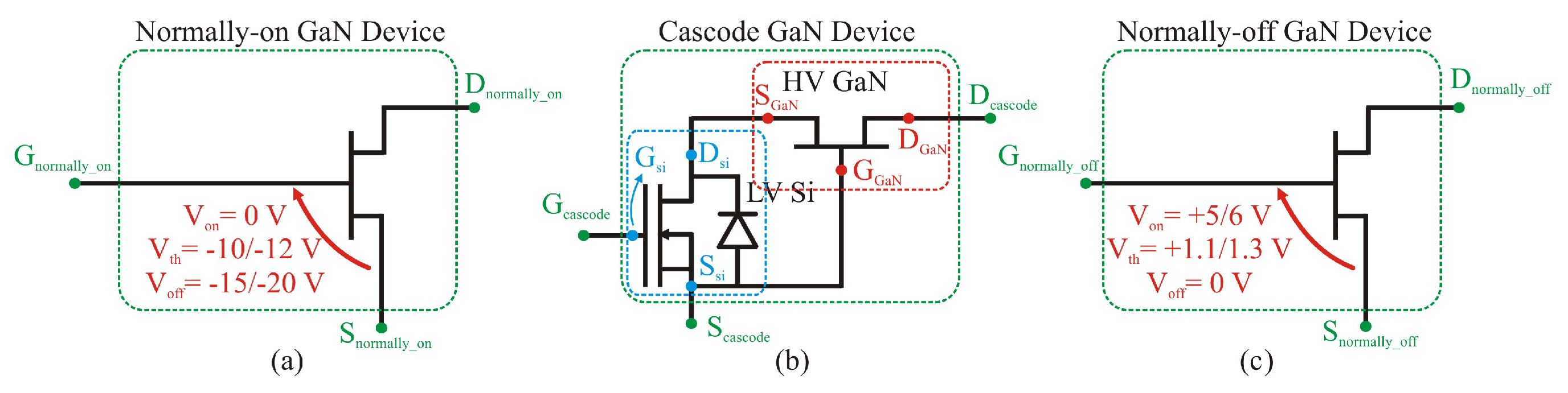
2.1. Depletion-Mode
2.2. Cascode-Mode
2.3. Enhancement-Mode
2.4. Comparison between GaN Structures
2.5. Advantages and Disadvantages of Each GaN Technology
- The normally-on device brings a cost benefit for manufacturers in terms of production, although presenting a limited amount of applications and gate-driver challenges (synchronization and/or extra safety) in order to have a safe operation. Possible applications include current-fed converters and converters with short-circuit protection schemes integrated.
- Cascode GaNs bring the benefit of normally-off devices with a higher threshold voltage. On the other hand, the devices present reverse recovery due to the LV Si MOSFET and higher on-resistance and internal parasitics compared with other GaN technologies. Since this component is more immune against gate oscillations (discussed in Section 3.1.3), this component is suited better in applications with multiple switches, e.g., multi-level converters and high step-up and step-down applications.
- Normally-off GaNs present the lowest gate charge and on-resistance compared with the aforementioned GaNs, while having the lowest threshold voltage. Thus, this component is more susceptible to malfunction due to gate-source ringing. Converters with ground connection to the source of the switch or limited floating points are the structure in which this device presents better performance, e.g., DC-DC boost converter, DC-DC buck converter, full-bridge, and half-bridge topologies.
3. Design/Layout Challenges
3.1. PCB Layout/Design
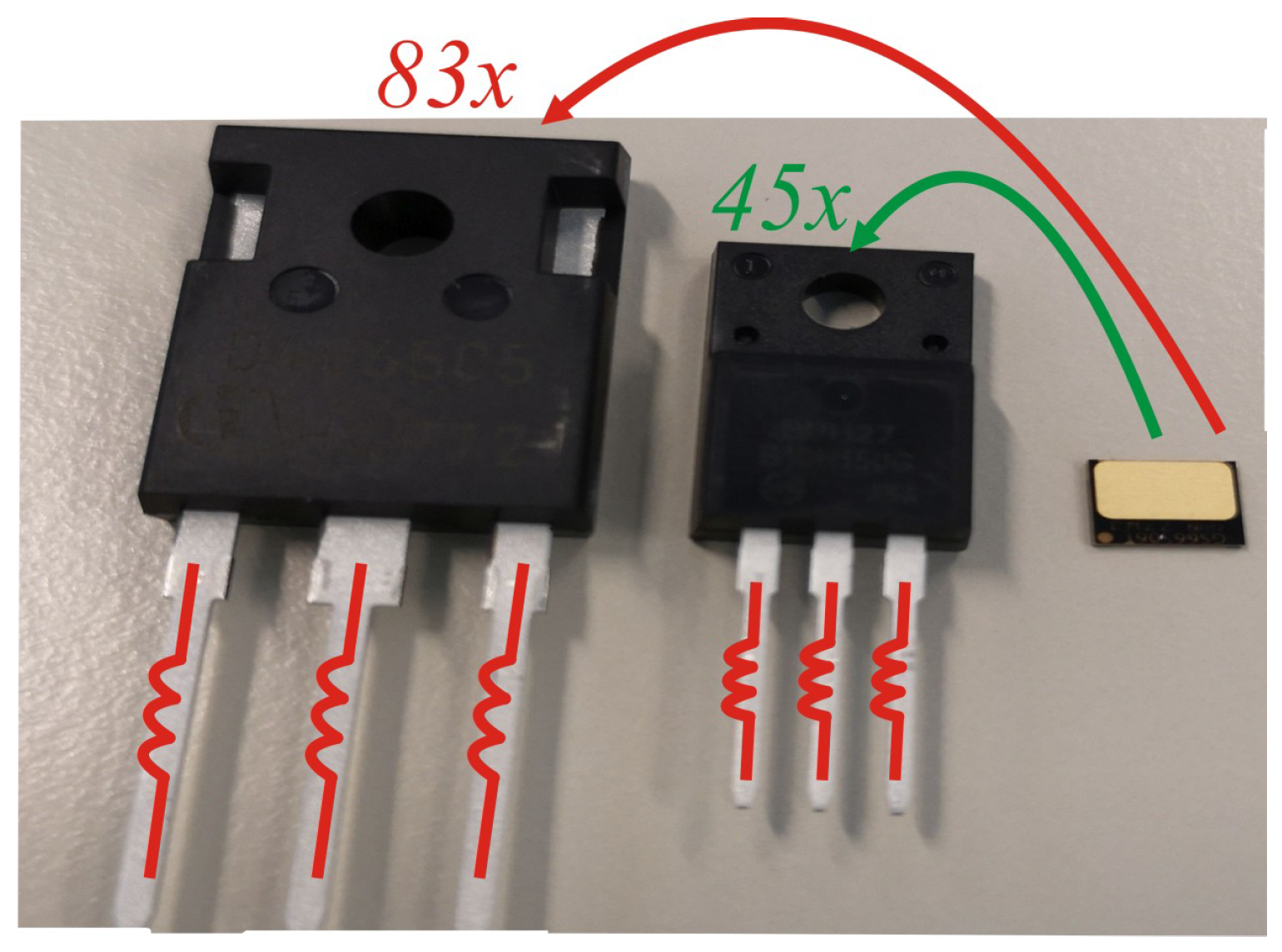
3.1.1. Device Package
3.1.2. Internal Parasitics
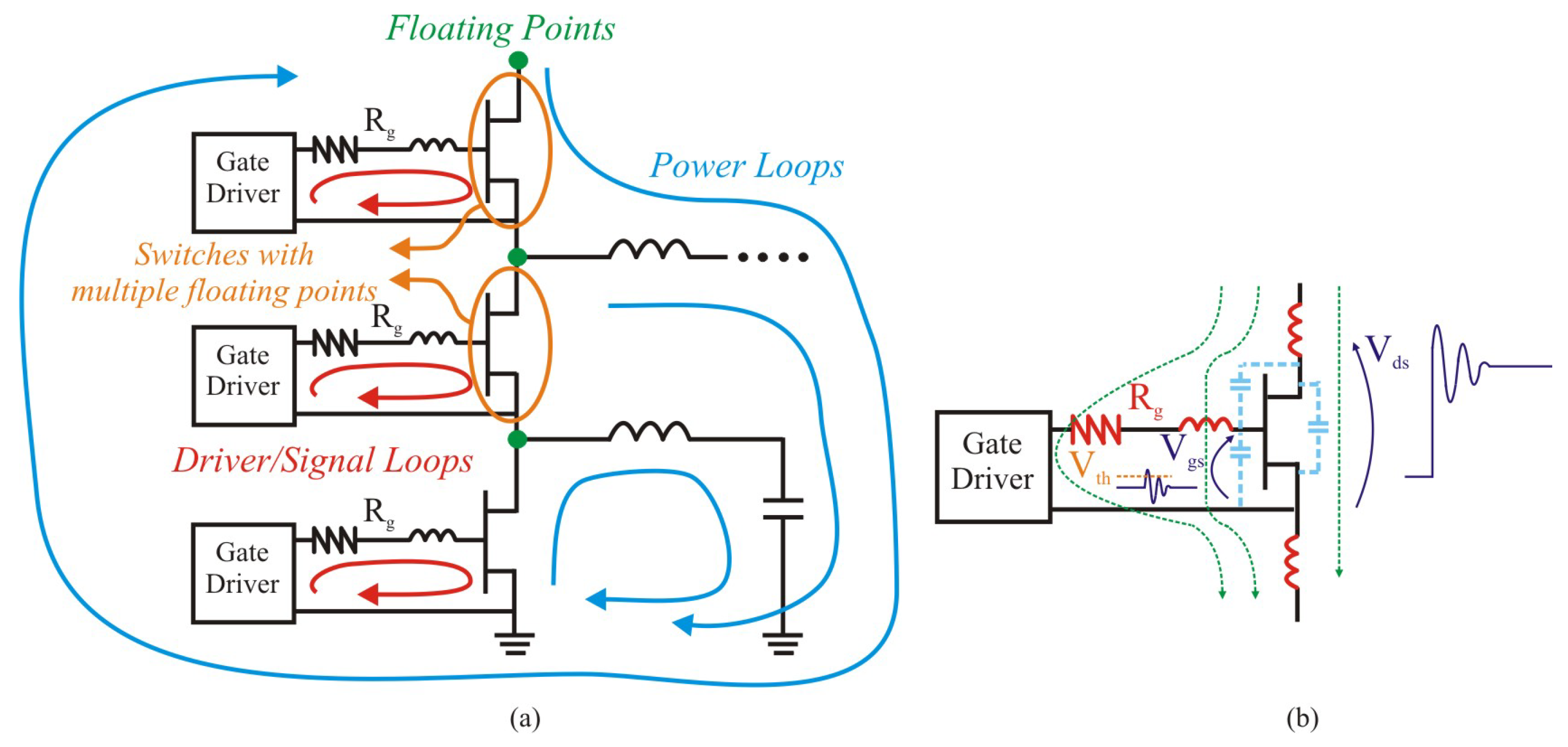
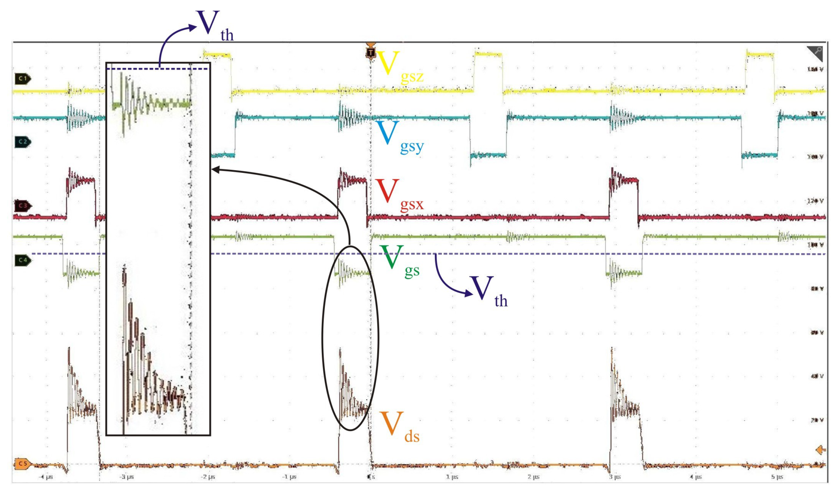
3.1.3. Signal and Power Loops
- PCB design is crucial to achieve the best performance of the GaN devices.
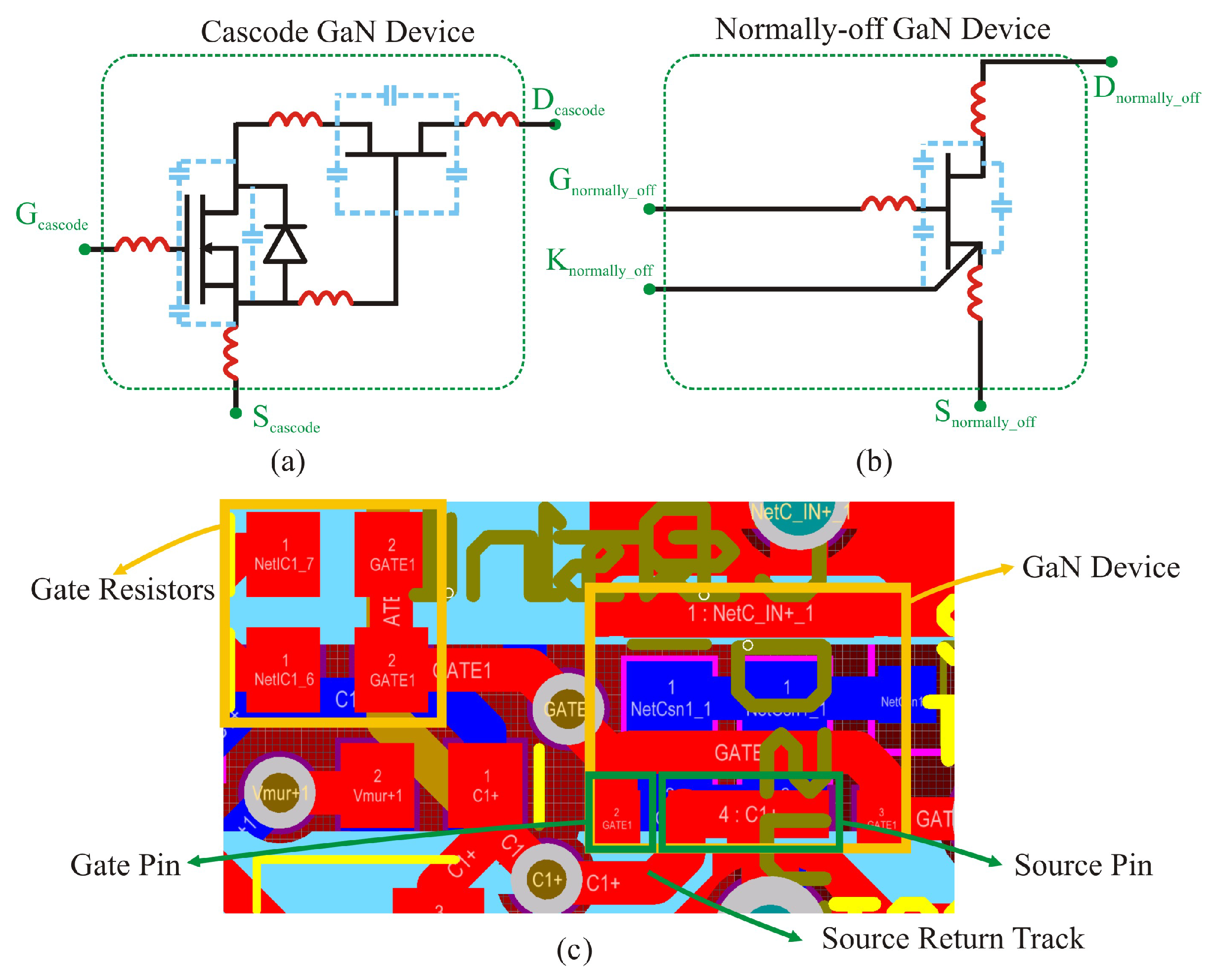
- Gate-resistors are used to control the speed of the device, and its placement during the design stage should be as close as possible to the gate pin of the GaN semiconductor. As mentioned above, monolithic integration of the switch and driver in the same package has been considered for the new generation of GaN power devices. Although this strategy brings the benefits of loops and parasitic minimization, mitigating voltage dips that might collapse the gate of these devices, it also takes away the freedom to control the rise and fall times of the switch by selecting the proper gate resistors. Additionally, these structures can be used to build simple topologies, e.g., buck, boost, buck-boost, and full-bridge. More complex structures still require separate switches and drivers.
- Components that present Kelvin connection internally decouple the common source inductance on the power stage of the device. For components that do not offer this extra pin, the gate return pad should be connected as close as possible to the gate of the GaN device, as shown in Figure 5, minimizing the parasitic inductances at the gate level.
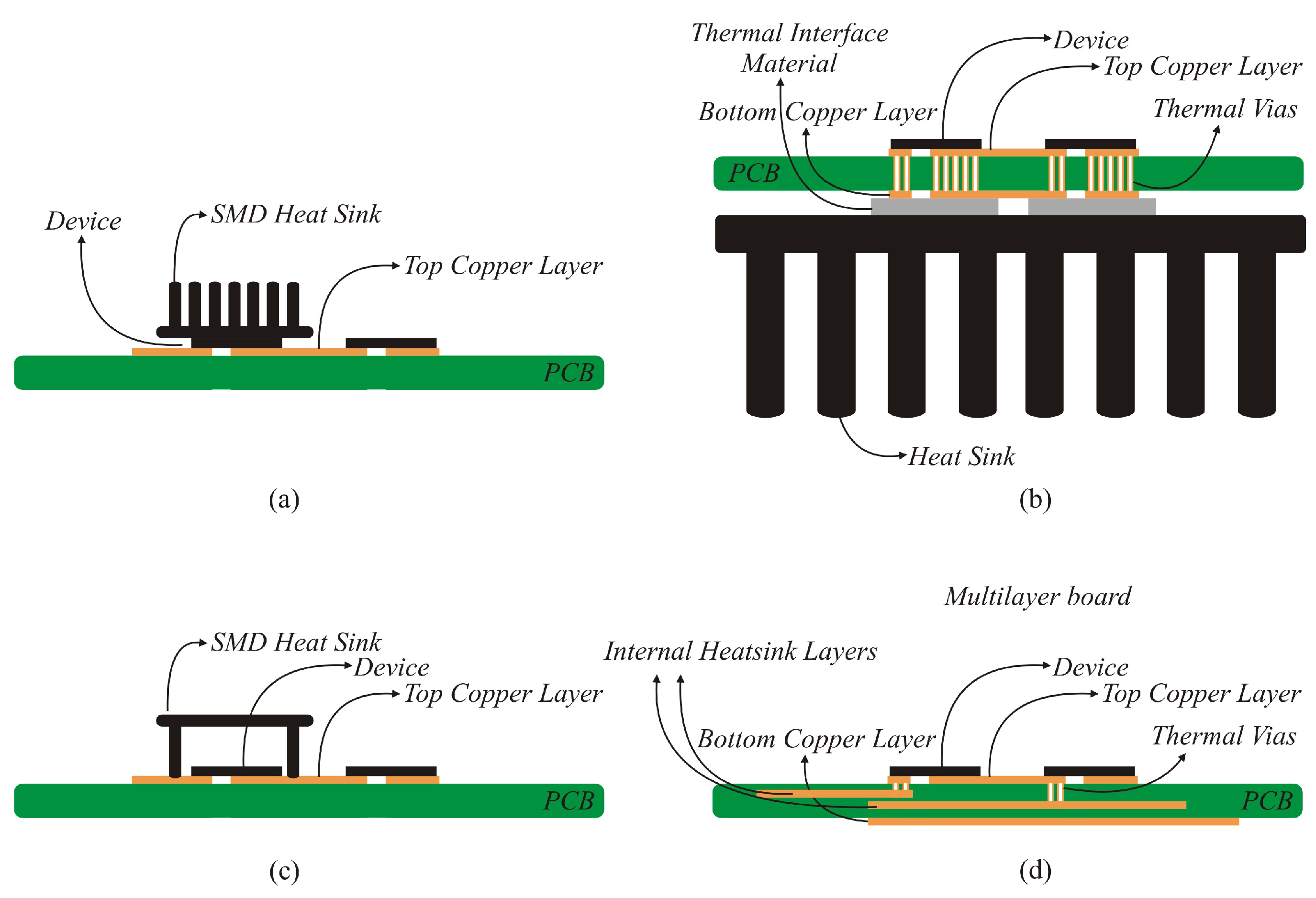
3.2. Thermal Management
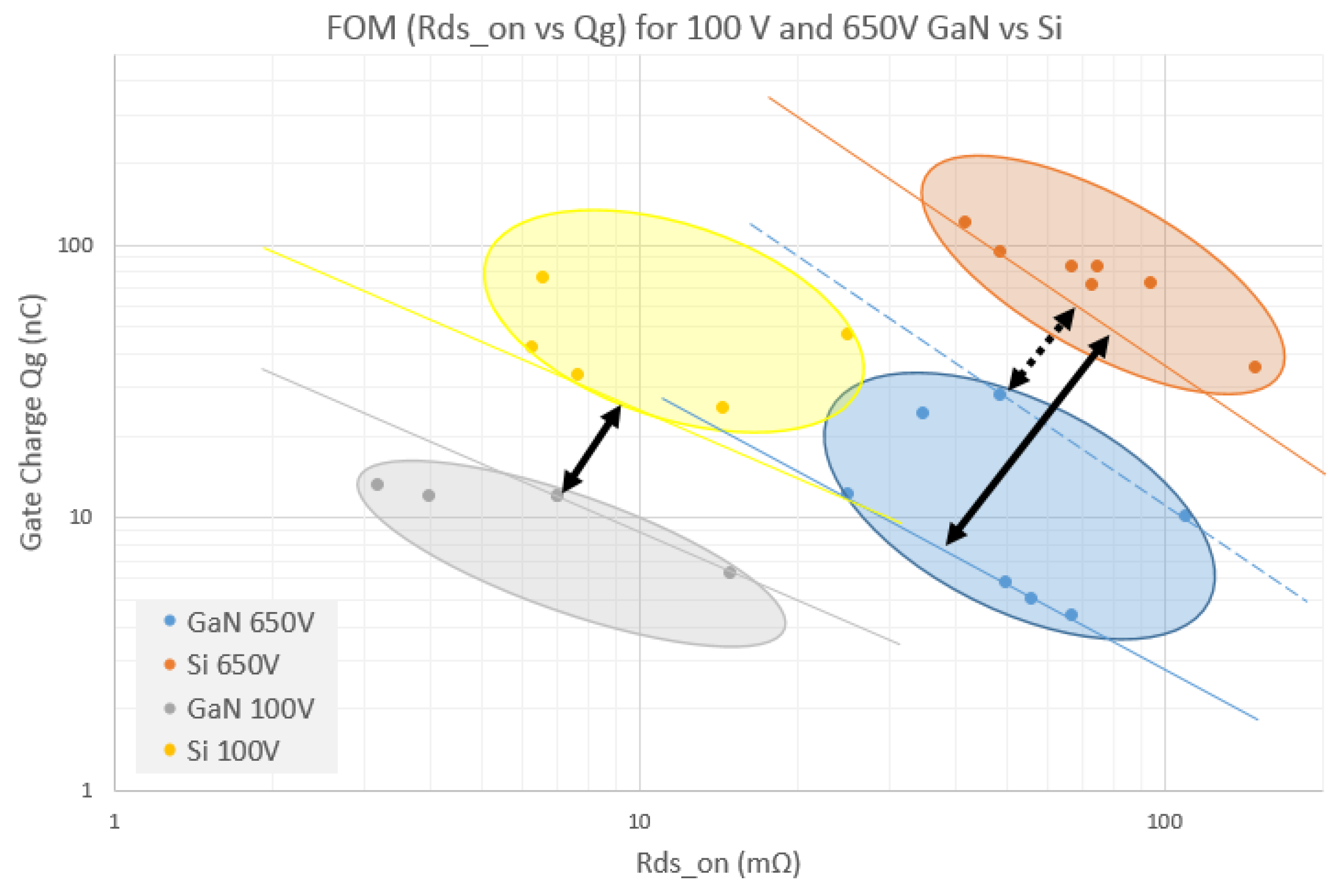
4. Comparison between GaN and Si Semiconductors
5. Conclusions
Author Contributions
Funding
Conflicts of Interest
References
- Tan, D. Emerging System Applications and Technological Trends in Power Electronics: Power electronics is increasingly cutting across traditional boundaries. IEEE Power Electron. Mag. 2015, 2, 38–47. [Google Scholar] [CrossRef]
- Dulău, L.I.; Abrudean, M.; Bică, D. Automation of a distributed generation system. In Proceedings of the 2014 49th International Universities Power Engineering Conference (UPEC), Cluj-Napoca, Romania, 2–5 September 2014; pp. 1–5. [Google Scholar] [CrossRef]
- Wang, C.; Nehrir, M.H. Distributed Generation Applications of Fuel Cells. In Proceedings of the 2006 Power Systems Conference: Advanced Metering, Protection, Control, Communication, and Distributed Resources, Clemson, SC, USA, 14–17 March 2006; pp. 244–248. [Google Scholar] [CrossRef]
- Chiradeja, P. Benefit of Distributed Generation: A Line Loss Reduction Analysis. In Proceedings of the 2005 IEEE/PES Transmission Distribution Conference Exposition: Asia and Pacific, Dalian, China, 18 August 2005; pp. 1–5. [Google Scholar] [CrossRef]
- Guerrero, J.M.; Berbel, N.; Matas, J.; de Vicuna, L.G.; Miret, J. Decentralized Control for Parallel Operation of Distributed Generation Inverters in Microgrids Using Resistive Output Impedance. In Proceedings of the IECON 2006—32nd Annual Conference on IEEE Industrial Electronics, Paris, France, 6–10 November 2006; pp. 5149–5154. [Google Scholar] [CrossRef]
- Du, W.; Chen, Z.; Wang, H.F.; Dunn, R. Energy storage systems applied in power system stability control. In Proceedings of the 2007 42nd International Universities Power Engineering Conference, Brighton, UK, 4–6 September 2007; pp. 455–458. [Google Scholar] [CrossRef]
- Ma, Y.; Chen, Y. Storage Systems Management Based on Big Data—Take Three Common Storage Systems as Examples. In Proceedings of the 2018 15th International Conference on Service Systems and Service Management (ICSSSM), Hangzhou, China, 21–22 July 2018; pp. 1–6. [Google Scholar] [CrossRef]
- Fei, C.; Lee, F.C.; Li, Q. High-Efficiency High-Power-Density LLC Converter With an Integrated Planar Matrix Transformer for High-Output Current Applications. IEEE Trans. Ind. Electron. 2017, 64, 9072–9082. [Google Scholar] [CrossRef]
- Huang, Q.; Huang, A.; Yu, R.; Liu, P.; Yu, W. High-Efficiency and High-Density Single-Phase Dual-Mode Cascaded Buck-Boost Multilevel Transformerless PV Inverter with GaN AC Switches. IEEE Trans. Power Electron. 2018. [Google Scholar] [CrossRef]
- Chen, R.; Yu, S. A high-efficiency high-power-density 1 MHz LLC converter with GaN devices and integrated transformer. In Proceedings of the 2018 IEEE Applied Power Electronics Conference and Exposition (APEC), San Antonio, TX, USA, 4–8 March 2018; pp. 791–796. [Google Scholar] [CrossRef]
- Ravyts, S.; Dalla Vecchia, M.; Zwysen, J.; van den Broeck, G.; Driesen, J. Comparison Between an Interleaved Boost Converter Using Si MOSFETs Versus GaN HEMTs. In Proceedings of the PCIM Europe 2018; International Exhibition and Conference for Power Electronics, Intelligent Motion, Renewable Energy and Energy Management, Nuremberg, Germany, 5–7 June 2018; pp. 1–8. [Google Scholar]
- Shamsi, P.; McDonough, M.; Fahimi, B. Wide-Bandgap Semiconductor Technology: Its impact on the electrification of the transportation industry. IEEE Electrif. Mag. 2013, 1, 59–63. [Google Scholar] [CrossRef]
- Bindra, A. Wide-Bandgap Power Devices: Adoption Gathers Momentum. IEEE Power Electron. Mag. 2018, 5, 22–27. [Google Scholar] [CrossRef]
- Dawon, K. Electric Field Controlled Semiconductor Device. U.S. Patent US3102230A, 27 August 1963. [Google Scholar]
- Andersen, T.M.; Krismer, F.; Kolar, J.W.; Toifl, T.; Menolfi, C.; Kull, L.; Morf, T.; Kossel, M.; Brändli, M.; Francese, P.A. Modeling and Pareto Optimization of On-Chip Switched Capacitor Converters. IEEE Trans. Power Electron. 2017, 32, 363–377. [Google Scholar] [CrossRef]
- Lefranc, P.; Odic, E.; Kirkpatrick, M.J. Optimisation and characterisation of a planar transformer with a high voltage ratio and high output voltage for plasma reactors. IET Power Electron. 2015, 8, 929–937. [Google Scholar] [CrossRef]
- Bosshard, R.; Kolar, J.W.; Mühlethaler, J.; Stevanović, I.; Wunsch, B.; Canales, F. Modeling and η-α-Pareto Optimization of Inductive Power Transfer Coils for Electric Vehicles. IEEE J. Emerg. Sel. Top. Power Electron. 2015, 3, 50–64. [Google Scholar] [CrossRef]
- Boillat, D.O.; Krismer, F.; Kolar, J.W. Design Space Analysis and ρ-η Pareto Optimization of LCO utput Filters for Switch-Mode AC Power Sources. IEEE Trans. Power Electron. 2015, 30, 6906–6923. [Google Scholar] [CrossRef]
- Baliga, B.J. Semiconductors for high-voltage, vertical channel field-effect transistors. J. Appl. Phys. 1982, 53, 1759–1764. [Google Scholar] [CrossRef]
- Baliga, B.J. Power semiconductor device figure of merit for high-frequency applications. IEEE Electron Dev. Lett. 1989, 10, 455–457. [Google Scholar] [CrossRef]
- Chow, T.P.; Omura, I.; Higashiwaki, M.; Kawarada, H.; Pala, V. Smart Power Devices and ICs Using GaAs and Wide and Extreme Bandgap Semiconductors. IEEE Trans. Electron Dev. 2017, 64, 856–873. [Google Scholar] [CrossRef]
- Hudgins, J.L.; Simin, G.S.; Santi, E.; Khan, M.A. An assessment of wide band gap semiconductors for power devices. IEEE Trans. Power Electron. 2003, 18, 907–914. [Google Scholar] [CrossRef]
- Shenai, K. Future Prospects of Wideband gap (WBG) Semiconductor Power Switching Devices. IEEE Trans. Electron Dev. 2015, 62, 248–257. [Google Scholar] [CrossRef]
- Lidow, A.; Strydom, J.; De Rooij, M.; Reusch, D. GaN Transistors for Efficient Power Conversion, 1st ed.; Wiley: Hoboken, NJ, USA, 2015. [Google Scholar]
- Park, B.; Han, S.; Cha, H. Diode Bridge Embedded AlGaN/GaN Bidirectional Switch. IEEE Electron Dev. Lett. 2015, 36, 324–326. [Google Scholar] [CrossRef]
- Mehrotra, V.; Arias, A.; Neft, C.; Bergman, J.; Urteaga, M.; Brar, B. GaN HEMT-Based> 1-GHz Speed Low-Side Gate Driver and Switch Monolithic Process for 865-MHz Power Conversion Applications. IEEE J. Emerg. Sel. Top. Power Electron. 2016, 4, 918–925. [Google Scholar] [CrossRef]
- Wang, X.; Mazumder, S.K.; Shi, W. A GaN-Based Insulated-Gate Photoconductive Semiconductor Switch for Ultrashort High-Power Electric Pulses. IEEE Electron Dev. Lett. 2015, 36, 493–495. [Google Scholar] [CrossRef]
- Ren, J.; Liu, C.; Tang, C.W.; Lau, K.M.; Sin, J.K.O. Switching characteristics of monolithically integrated Si-GaN cascoded rectifiers. In Proceedings of the 2017 29th International Symposium on Power Semiconductor Devices and IC’s (ISPSD), Sapporo, Japan, 28 May–1 June 2017; pp. 223–226. [Google Scholar] [CrossRef]
- Horikiri, F.; Narita, Y.; Yoshida, T.; Kitamura, T.; Ohta, H.; Nakamura, T.; Mishima, T. Wafer-Level Donor Uniformity Improvement by Substrate Off-Angle Control for Vertical GaN-on-GaN Power Switching Devices. IEEE Trans. Semicond. Manuf. 2017, 30, 486–493. [Google Scholar] [CrossRef]
- Ruzzarin, M.; Meneghini, M.; Bisi, D.; Sun, M.; Palacios, T.; Meneghesso, G.; Zanoni, E. Instability of Dynamic- RON and Threshold Voltage in GaN-on-GaN Vertical Field-Effect Transistors. IEEE Trans. Electron Dev. 2017, 64, 3126–3131. [Google Scholar] [CrossRef]
- Han, S.; Noh, Y.; Jo, M.; Kim, S.; Oh, J.; Seo, K.; Cha, H. Normally-Off MOS-HFET on AlGaN/GaN-on-Si(110) Grown by NH3MBE. IEEE Electron Dev. Lett. 2016, 37, 1613–1616. [Google Scholar] [CrossRef]
- Medjdoub, F.; Hove, M.V.; Cheng, K.; Marcon, D.; Leys, M.; Decoutere, S. Novel E-Mode GaN-on-Si MOSHEMT Using a Selective Thermal Oxidation. IEEE Electron Dev. Lett. 2010, 31, 948–950. [Google Scholar] [CrossRef]
- Cao, L.; Lo, C.; Marchand, H.; Johnson, W.; Fay, P. Low-Loss Coplanar Waveguides on GaN-on-Si Substrates. IEEE Microw. Wirel. Compon. Lett. 2018, 28, 861–863. [Google Scholar] [CrossRef]
- Dong, M.; Elmes, J.; Peper, M.; Batarseh, I.; Shen, Z.J. Investigation on inherently safe gate drive techniques for normally-on wide band gap power semiconductor switching devices. In Proceedings of the 2009 IEEE Energy Conversion Congress and Exposition, San Jose, CA, USA, 20–24 September 2009; pp. 120–125. [Google Scholar] [CrossRef]
- Vecchia, M.D.; den Broeck, G.V.; Ravyts, S.; Driesen, J. Application of a 100 A normally-on GaN-based device in a 2 kW/400 V input half-bridge non-isolated DC-DC configuration. In Proceedings of the 2017 IEEE 5th Workshop on Wide Bandgap Power Devices and Applications (WiPDA), Albuquerque, NM, USA, 30 October–1 November 2017; pp. 111–115. [Google Scholar] [CrossRef]
- Okamoto, M.; Tanaka, T.; Matuzaki, K.; Hashizume, T.; Yamada, H. 13.56-MHz Class-E RF power amplifier using normally-on GaN HEMT. In Proceedings of the IECON 2014—40th Annual Conference of the IEEE Industrial Electronics Society, Dallas, TX, USA, 29 October–1 November 2014; pp. 982–987. [Google Scholar] [CrossRef]
- Jacqmaer, P.; Everts, J.; Gelagaev, R.; Tant, P.; Driesen, J. Fast robust gate-drivers with easily adjustable voltage ranges for driving normally-on wide-band gap power transistors. In Proceedings of the 14th International Power Electronics and Motion Control Conference EPE-PEMC 2010, Ohrid, Macedonia, 6–8 September 2010; pp. T2-44–T2-51. [Google Scholar] [CrossRef]
- Okamoto, M.; Ishibashi, T.; Yamada, H.; Tanaka, T. Resonant Gate Driver for a Normally ON GaN HEMT. IEEE J. Emerg. Sel. Top. Power Electron. 2016, 4, 926–934. [Google Scholar] [CrossRef]
- Ishibashi, T.; Okamoto, M.; Hiraki, E.; Tanaka, T.; Hashizume, T.; Kikuta, D.; Kachi, T. Experimental validation of newly fabricated normally-on GaN high-electron-mobility transistor. In Proceedings of the 2013 IEEE Energy Conversion Congress and Exposition, Denver, CO, USA, 15–19 September 2013; pp. 1584–1591. [Google Scholar] [CrossRef]
- Ishibashi, T.; Okamoto, M.; Hiraki, E.; Tanaka, T.; Hashizume, T.; Kikuta, D.; Kachi, T. Experimental Validation of Normally-On GaN HEMT and Its Gate Drive Circuit. IEEE Trans. Ind. Appl. 2015, 51, 2415–2422. [Google Scholar] [CrossRef]
- Zhang, W.; Huang, X.; Liu, Z.; Lee, F.C.; She, S.; Du, W.; Li, Q. A New Package of High-Voltage Cascode Gallium Nitride Device for Megahertz Operation. IEEE Trans. Power Electron. 2016, 31, 1344–1353. [Google Scholar] [CrossRef]
- Liu, Z.; Huang, X.; Lee, F.C.; Li, Q. Package Parasitic Inductance Extraction and Simulation Model Development for the High-Voltage Cascode GaN HEMT. IEEE Trans. Power Electron. 2014, 29, 1977–1985. [Google Scholar] [CrossRef]
- Li, H.; Zhang, X.; Wen, L.; Brothers, J.A.; Yao, C.; Han, C.; Liu, L.; Xu, J.; Puukko, J.; Wang, J. Paralleled Operation of High-Voltage Cascode GaN HEMTs. IEEE J. Emerg. Sel. Top. Power Electron. 2016, 4, 815–823. [Google Scholar] [CrossRef]
- Jung, D.Y.; Park, Y.; Lee, H.S.; Jun, C.H.; Jang, H.G.; Park, J.; Kim, M.; Ko, S.C.; Nam, E.S. Design and Evaluation of Cascode GaN FET for Switching Power Conversion Systems. ETRI J. 2017, 39, 62–68. [Google Scholar] [CrossRef]
- Chellappan, S. Design Considerations of GaN Devices for Improving Power Converter Efficiency; Texas Instruments Inc.: Dallas, TX, USA, 2017. [Google Scholar]
- Transphorm GaN Power FET Portfolio. Available online: https://www.transphormusa.com/en/products/ (accessed on 5 December 2018).
- GS66506T. Available online: https://gansystems.com/gan-transistors/gs66506t/ (accessed on 6 November 2018).
- GS-065-120-1-D. Available online: https://gansystems.com/gan-transistors/gs-065-120-1-d/ (accessed on 6 November 2018).
- Mueller, C.R.; Buschhorn, S. Impact of module parasitics on the performance of fastswitching devices. In Proceedings of the PCIM Europe 2014; International Exhibition and Conference for Power Electronics, Intelligent Motion, Renewable Energy and Energy Management, Nuremberg, Germany, 20–22 May 2014; pp. 1–8. [Google Scholar]
- Zhang, Z.; Guo, B.; Wang, F. Evaluation of Switching Loss Contributed by Parasitic Ringing for Fast Switching Wide Band-Gap Devices. IEEE Trans. Power Electron. 2018. [Google Scholar] [CrossRef]
- Reusch, D. Impact of Parasitics on Performance. 2013, p. 5. Available online: https://epc-co.com/epc/Portals/0/epc/documents/papers/ImpactofParasitcsonPerformance.pdf (accessed on 17 December 2018).
- Lu, J.; Bai, H.; Brown, A.; McAmmond, M.; Chen, D.; Styles, J. Design consideration of gate driver circuits and PCB parasitic parameters of paralleled E-mode GaN HEMTs in zero-voltage-switching applications. In Proceedings of the 2016 IEEE Applied Power Electronics Conference and Exposition (APEC), Long Beach, CA, USA, 20–24 March 2016; pp. 529–535. [Google Scholar] [CrossRef]
- Nayak, P.; Hatua, K. Parasitic Inductance and Capacitance-Assisted Active Gate Driving Technique to Minimize Switching Loss of SiC MOSFET. IEEE Trans. Ind. Electron. 2017, 64, 8288–8298. [Google Scholar] [CrossRef]
- Huang, X.; Li, Q.; Liu, Z.; Lee, F.C. Analytical loss model of high voltage GaN HEMT in cascode configuration. In Proceedings of the 2013 IEEE Energy Conversion Congress and Exposition, Denver, CO, USA, 15–19 September 2013; pp. 3587–3594. [Google Scholar] [CrossRef]
- Huang, X.; Li, Q.; Liu, Z.; Lee, F.C. Analytical Loss Model of High Voltage GaN HEMT in Cascode Configuration. IEEE Trans. Power Electron. 2014, 29, 2208–2219. [Google Scholar] [CrossRef]
- Lidow, A.; Strydom, J.; Strittmatter, R.; Zhou, C. GaN: A Reliable Future in Power Conversion: Dramatic performance improvements at a lower cost. IEEE Power Electron. Mag. 2015, 2, 20–26. [Google Scholar] [CrossRef]
- Wang, J.; Chung, H.S.H. Impact of Parasitic Elements on the Spurious Triggering Pulse in Synchronous Buck Converter. IEEE Trans. Power Electron. 2014, 29, 6672–6685. [Google Scholar] [CrossRef]
- Index of/Application-Notes/AN. Available online: https://www.fairchildsemi.com/application-notes/AN/ (accessed on 2 January 2019).
- Tibola, G.; Lemmen, E.; Duarte, J.L.; Barbi, I. Passive Regenerative and Dissipative Snubber Cells for Isolated SEPIC Converters: Analysis, Design, and Comparison. IEEE Trans. Power Electron. 2017, 32, 9210–9222. [Google Scholar] [CrossRef]
- Finney, S.J.; Williams, B.W.; Green, T.C. RCD snubber revisited. IEEE Trans. Ind. Appl. 1996, 32, 155–160. [Google Scholar] [CrossRef]
- Yatsugi, K.; Nomura, K.; Hattori, Y. Analytical Technique for Designing an RC Snubber Circuit for Ringing Suppression in a Phase-Leg Configuration. IEEE Trans. Power Electron. 2018, 33, 4736–4745. [Google Scholar] [CrossRef]
- Ujita, S.; Kinoshita, Y.; Umeda, H.; Morita, T.; Kaibara, K.; Tamura, S.; Ishida, M.; Ueda, T. A fully integrated GaN-based power IC including gate drivers for high-efficiency DC-DC Converters. In Proceedings of the 2016 IEEE Symposium on VLSI Circuits (VLSI-Circuits), Honolulu, HI, USA, 15–17 June 2016; pp. 1–2. [Google Scholar] [CrossRef]
- Cool-Power ZVS Buck Regulators. Available online: http://www.vicorpower.com/dc-dc-converters-board-mount/cool-power-pi33xx-and-pi34xx (accessed on 17 December 2018).
- LMG3410R070 600-V 70 mΩ GaN With Integrated Driver and Protection|TI.com. Available online: http://www.ti.com/product/LMG3410R070 (accessed on 18 December 2018).
- EPC2115: Dual 150 V, 5 A Integrated Gate Drivers eGaN IC. Available online: https://epc-co.com/epc/Products/eGaNFETsandICs/EPC2115.aspx (accessed on 17 December 2018).
- Choi, S.; Heller, E.R.; Dorsey, D.; Vetury, R.; Graham, S. The Impact of Bias Conditions on Self-Heating in AlGaN/GaN HEMTs. IEEE Trans. Electron Dev. 2013, 60, 159–162. [Google Scholar] [CrossRef]
- Yang, L.; Chen, Z.; Xu, X.; Zhang, J. Study on the Heat Transfer of GaN-Based High Power HEMTs. IEEE Trans. Semicond. Manuf. 2017, 30, 526–530. [Google Scholar] [CrossRef]
- AlOtaibi, B.; Valizadeh, P. Investigation of the High-Temperature Operation of AlGaN/GaN HFETs via Studying the Impact of Temperature Dependency of Drift Transport Characteristics. IEEE Trans. Dev. Mater. Reliab. 2012, 12, 547–553. [Google Scholar] [CrossRef]
- Lu, X.; Ma, J.; Yue, C.P.; Lau, K.M. A GaN-Based Lamb-Wave Oscillator on Silicon for High-Temperature Integrated Sensors. IEEE Microw. Wirel. Compon. Lett. 2013, 23, 318–320. [Google Scholar] [CrossRef]
- Maier, D.; Alomari, M.; Grandjean, N.; Carlin, J.; Diforte-Poisson, M.; Dua, C.; Chuvilin, A.; Troadec, D.; Gaquiere, C.; Kaiser, U.; et al. Testing the Temperature Limits of GaN-Based HEMT Devices. IEEE Trans. Dev. Mater. Reliab. 2010, 10, 427–436. [Google Scholar] [CrossRef]
- Cuerdo, R.; Sillero, E.; Romero, M.F.; Uren, M.J.; di Forte Poisson, M.; Munoz, E.; Calle, F. High-Temperature Microwave Performance of Submicron AlGaN/GaN HEMTs on SiC. IEEE Electron Dev. Lett. 2009, 30, 808–810. [Google Scholar] [CrossRef]
- Roder, C.; Einfeldt, S.; Figge, S.; Hommel, D. Temperature dependence of the thermal expansion of GaN. Phys. Rev. B 2005, 72, 085218. [Google Scholar] [CrossRef]
- Bernard, K. Advantages of Using Gallium NitrideFETs in Satellite Applications; Renesas: Tokyo, Japan, 2018. [Google Scholar]
- Ando, Y.; Ishikura, K.; Murase, Y.; Asano, K.; Takenaka, I.; Takahashi, S.; Takahashi, H.; Sasaoka, C. Impact of Epi-Layer Quality on Reliability of GaN/AlGaN/GaN Heterostructure Field-Effect Transistors on Si Substrate. IEEE Trans. Electron Dev. 2013, 60, 4125–4132. [Google Scholar] [CrossRef]
- Lee, C.; Witkowski, L.; Tserng, H.; Saunier, P.; Birkhahn, R.; Olson, D.; Olson, D.; Munns, G.; Guo, S.; Albert, B. Effects of AlGaN/GaN HEMT structure on RF reliability. Electron. Lett. 2005, 41, 155–157. [Google Scholar] [CrossRef]
- Zanoni, E.; Meneghini, M.; Chini, A.; Marcon, D.; Meneghesso, G. AlGaN/GaN-Based HEMTs Failure Physics and Reliability: Mechanisms Affecting Gate Edge and Schottky Junction. IEEE Trans. Electron Dev. 2013, 60, 3119–3131. [Google Scholar] [CrossRef]
- Kwan, A.M.H.; Chen, K.J. A Gate Overdrive Protection Technique for Improved Reliability in AlGaN/GaN Enhancement-Mode HEMTs. IEEE Electron Dev. Lett. 2013, 34, 30–32. [Google Scholar] [CrossRef]
- Sun, H.; Pomeroy, J.W.; Simon, R.B.; Francis, D.; Faili, F.; Twitchen, D.J.; Kuball, M. Temperature-Dependent Thermal Resistance of GaN-on-Diamond HEMT Wafers. IEEE Electron Dev. Lett. 2016, 37, 621–624. [Google Scholar] [CrossRef]
- Chou, H.P.; Ho, C.H.; Cheng, Y.J.; Chou, P.C.; Cheng, S. A new high power device of GaN HEMTs on Si substrate with lateral heat dissipation packaging. In Proceedings of the 2012 IEEE 13th Workshop on Control and Modeling for Power Electronics (COMPEL), Kyoto, Japan, 10–13 June 2012; pp. 1–5. [Google Scholar] [CrossRef]
- Yu, C.; Labouré; Buttay, C. Thermal management of lateral GaN power devices. In Proceedings of the 2015 IEEE International Workshop on Integrated Power Packaging (IWIPP), Chicago, IL, USA, 3–6 May 2015; pp. 40–43. [Google Scholar] [CrossRef]
- GS66508P. Available online: https://gansystems.com/gan-transistors/gs66508p/ (accessed on 9 November 2018).
- Shenai, K. The Figure of Merit of a Semiconductor Power Electronics Switch. IEEE Trans. Electron Dev. 2018, 65, 4216–4224. [Google Scholar] [CrossRef]
- Kim, I.J.; Matsumoto, S.; Sakai, T.; Yachi, T. New power device figure of merit for high-frequency applications. In Proceedings of the International Symposium on Power Semiconductor Devices and IC’s: ISPSD ’95, Yokohama, Japan, 23–25 May 1995; pp. 309–314. [Google Scholar] [CrossRef]
- Wang, H.; Wang, F.; Zhang, J. Power Semiconductor Device Figure of Merit for High-Power-Density Converter Design Applications. IEEE Trans. Electron Dev. 2008, 55, 466–470. [Google Scholar] [CrossRef]
- Huang, A.Q. New unipolar switching power device figures of merit. IEEE Electron Dev. Lett. 2004, 25, 298–301. [Google Scholar] [CrossRef]
- Keyes, R.W. Figure of merit for semiconductors for high-speed switches. Proc. IEEE 1972, 60, 225. [Google Scholar] [CrossRef]
- De Vreede, L.C.N.; de Graaff, H.C.; Hurkx, G.A.M.; Tauritz, J.L.; Baets, R.G.F. A figure of merit for the high-frequency noise behavior of bipolar transistors. IEEE J. Solid-State Circuits 1994, 29, 1220–1226. [Google Scholar] [CrossRef]
- STW28N65M2 STMicroelectronics|Mouser. Available online: https://www.mouser.be/ProductDetail/511-STW28N65M2 (accessed on 8 November 2018).
- STF28N65M2 STMicroelectronics|Mouser. Available online: https://www.mouser.be/ProductDetail/511-STF28N65M2 (accessed on 8 November 2018).
- STL33N65M2 STMicroelectronics|Mouser. Available online: https://www.mouser.be/ProductDetail/511-STL33N65M2 (accessed on 8 November 2018).
- PGA26E19BA Product Overview. Available online: https://www.mouser.be/datasheet/2/315/pga26e19ba-product-standards-1112740.pdf (accessed on 30 November 2018).
- AG, I.T. Gallium Nitride (GaN)—Infineon Technologies. Available online: https://www.infineon.com/cms/en/product/power/wide-band-gap-semiconductors-sic-gan/gallium-nitride-gan/ (accessed on 30 November 2018).
- PGA26E07BA Product Overview. Available online: https://www.mouser.be/datasheet/2/315/pga26e07ba-product-standards-1112741.pdf (accessed on 30 November 2018).
- GS61004B. Available online: https://gansystems.com/gan-transistors/gs61004b/ (accessed on 8 November 2018).
- EPC2032. Available online: https://epc-co.com/epc/Products/eGaNFETsandICs/EPC2032.aspx (accessed on 8 November 2018).
- FDMS86152 ON Semiconductor/Fairchild|Mouser. Available online: https://www.mouser.be/ProductDetail/512-FDMS86152 (accessed on 8 November 2018).
- STF110N10F7 STMicroelectronics|Mouser. Available online: https://www.mouser.be/ProductDetail/511-STF110N10F7 (accessed on 8 November 2018).
- STI45N10F7 STMicroelectronics|Mouser. Available online: https://www.mouser.be/ProductDetail/511-STI45N10F7 (accessed on 8 November 2018).


| GaN Technology | Criteria | |||||||
|---|---|---|---|---|---|---|---|---|
| Ref. | V (V) | I (A) | (nC) | (V) | Package | (nC) | ||
| Normally-on | [40] | 600 | 2 | 0.16 | - | −6 | - | - |
| [35] | 650 | 100 | 0.017 | - | −10 | SMD | - | |
| Cascode | [46] | 650 | 20 | 0.110 | 54 | 2.1 | TO-220 | 10 |
| Normally-off | [47] | 650 | 22.5 | 0.067 | 0 | 1.1/1.3 | SMD | 5.8 |
| [48] | 650 | 120 | 0.012 | - | - | - | 25 | |
| Tech. | Criteria | ||||||||||||
|---|---|---|---|---|---|---|---|---|---|---|---|---|---|
| Ref. | V (V) | I (A) | (nC) | (nC) | (V) | Package (mm) | ( | (nC) | FOM1 | FOM2 [83] | FOM3 [84] | ||
| GaN | [46] | 650 | 20 | 0.110 | 54 | 2.9 | 56 | 10.25 × 8.7 | 1.3 | 10 | 1.1 | 6.16 | 0.01527 |
| GaN | [47] | 650 | 22.5 | 0.067 | 0 | 1.3 | 49 | 5.55 × 4.48 | 0.7 | 5.8 | 0.3886 | 3.283 | 0.19468 |
| GaN | [81] | 650 | 30 | 0.050 | 0 | 1.8 | 57 | 10.05 × 8.68 | 0.5 | 5.8 | 0.29 | 2.85 | 0.07642 |
| GaN | [35] | 650 | 100 | 0.017 | - | - | - | - | - | - | - | - | - |
| GaN | [48] | 650 | 120 | 0.012 | - | - | - | - | - | 25 | 0.3 | - | - |
| GaN | [91] | 600 | 13 | 0.140 | 0 | 1 | 28 | 8 × 8 | 1 | 2.0 | 0.28 | 3.92 | 0.02198 |
| GaN | [92] | 600 | 15 | 0.055 | 0 | - | 72 | 8 × 8 | 1.1 | 5.8 | 0.319 | 3.96 | - |
| GaN | [93] | 600 | 26 | 0.056 | 0 | 2.6 | 71 | 8 × 8 | 1.3 | 5.0 | 0.28 | 3.976 | 0.03149 |
| GaN | [92] | 600 | 31 | 0.055 | 0 | - | 72 | 15.9 × 11 | 1 | 5.8 | 0.319 | 3.96 | - |
| Si | [88] | 650 | 20 | 0.150 | 8200 | 15 | 60 | 20 × 15.5 | 0.74 | 35 | 5.25 | 9 | 0.0029 |
| Si | [89] | 650 | 20 | 0.150 | 5700 | 15 | 60 | 10.2 × 9.15 | 0.74 | 35 | 5.25 | 9 | 0.00965 |
| Si | [90] | 650 | 20 | 0.124 | 10,000 | 18 | 75 | 8 × 8 | 0.83 | 41.5 | 5.146 | 9.3 | 0.0126 |
| GaN | [94] | 100 | 45 | 0.015 | 0 | 0.9 | 140 | 4.6 × 4.4 | 1.1 | 6.2 | 0.093 | 2.1 | 0.38657 |
| GaN | [95] | 100 | 48 | 0.004 | 0 | 2 | 800 | 4.6 × 1 | 0.45 | 512 | 0.048 | 3.2 | 5.40 |
| Si | [96] | 100 | 45 | 0.0073 | 74 | 7.2 | 595 | 6.1 × 5 | 1 | 36 | 0.2628 | 4.3435 | 0.143 |
| Si | [97] | 100 | 45 | 0.0051 | 150 | 16 | 992 | 10.2 × 9.15 | 1 | 72 | 0.3672 | 5.0592 | 0.03751 |
| Si | [98] | 100 | 45 | 0.0145 | 67 | 12.2 | 360 | 10.2 × 9.15 | 2.5 | 25 | 0.3625 | 5.22 | 0.01019 |
© 2019 by the authors. Licensee MDPI, Basel, Switzerland. This article is an open access article distributed under the terms and conditions of the Creative Commons Attribution (CC BY) license (http://creativecommons.org/licenses/by/4.0/).
Share and Cite
Dalla Vecchia, M.; Ravyts, S.; Van den Broeck, G.; Driesen, J. Gallium-Nitride Semiconductor Technology and Its Practical Design Challenges in Power Electronics Applications: An Overview. Energies 2019, 12, 2663. https://doi.org/10.3390/en12142663
Dalla Vecchia M, Ravyts S, Van den Broeck G, Driesen J. Gallium-Nitride Semiconductor Technology and Its Practical Design Challenges in Power Electronics Applications: An Overview. Energies. 2019; 12(14):2663. https://doi.org/10.3390/en12142663
Chicago/Turabian StyleDalla Vecchia, Mauricio, Simon Ravyts, Giel Van den Broeck, and Johan Driesen. 2019. "Gallium-Nitride Semiconductor Technology and Its Practical Design Challenges in Power Electronics Applications: An Overview" Energies 12, no. 14: 2663. https://doi.org/10.3390/en12142663
APA StyleDalla Vecchia, M., Ravyts, S., Van den Broeck, G., & Driesen, J. (2019). Gallium-Nitride Semiconductor Technology and Its Practical Design Challenges in Power Electronics Applications: An Overview. Energies, 12(14), 2663. https://doi.org/10.3390/en12142663