1. Introduction
In recent years, rechargeable batteries have been widely used in many applications, including energy storage systems (ESS), electric vehicles (EV), and photo voltaic (PV) systems. Among these, lithium-ion batteries (LIBs) in particular have high power density, high energy density, and a long life cycle [
1,
2], meaning they are widely used to store energy. However, a single LIB cell has a low voltage and low capacity, so LIB packs are fabricated by connecting the cells in series and in parallel. However, manufacturing is inconsistent and usage environments differ [
3,
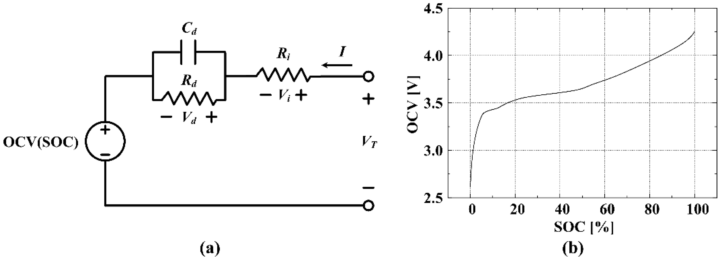
4], causing voltage and capacity to differ among cells in a battery string. This variability means that all serially connected cells cannot be simultaneously charged or discharged within the safe operating area (SOA), which is the region between charging voltage limit (CVL) and discharging voltage limit (DVL) (
Figure 1); the total capacity of the battery pack is determined by the strongest or weakest cell [
5]. Therefore, the battery pack requires a balancing circuit which evens the capacities of the batteries [
6,
7,
8,
9,
10,
11,
12,
13,
14,
15,
16,
17,
18,
19,
20,
21,
22,
23,
24,
25,
26].
Balancing circuits can be classified into passive type and active type. A passive balancing circuit dissipates the excessive energy of cells by using only shunt resistors, so the method is inexpensive and easy to control. However, the shunt resistor undergoes thermal heating, which can damage the battery pack, and the need to avoid this damage constrains the speed and energy-efficiency of the balancing operation [
6,
7]. In contrast, an active balancing circuit transfers the excess energy from the strong cells to the weak ones, making it a fast and energy-efficient way to balance the batteries [
8,
9,
10,
11,
12,
13,
14,
15,
16,
17,
18,
19,
20,
21,
22,
23,
24,
25,
26].
Many types of active balancing circuits have been reported; these transfer the charge from cell to pack [
8,
9], from pack to cell [
10,
11,
12], or from cell to cell [
13,
14,
15,
16,
17,
18,
19,
20]. Cell-to-pack balancing circuits are appropriate to balance strong cells during charging. Pack-to-cell balancing circuits are appropriate to balance weak cells during discharging. Cell-to-cell balancing circuits can balance battery cells during both charging and discharging, but most circuits of this type can only transfer the charge between adjacent cells [
13,
14,
15,
16]; i.e., the balancing energy may be delivered through irrelevant cells. This extended routing limits the power-transfer efficiency and increases the time required to achieve balance. Some active balancing circuits such as those of the bidirectional flyback type [
17], LC resonant type [
18,
19] and buck-boost type [
20] can directly transfer energy between any cells in a battery string. However, these active balancing circuits have limited balancing power and speed and they may not be able to balance all batteries in high-voltage applications. To solve these problems, modularized and multi-layer equalizers have been introduced [
21,
22,
23,
24,
25,
26]. These can achieve a high balancing power rate and a short balancing time but need many active components, complex control algorithms, and a high computational load.
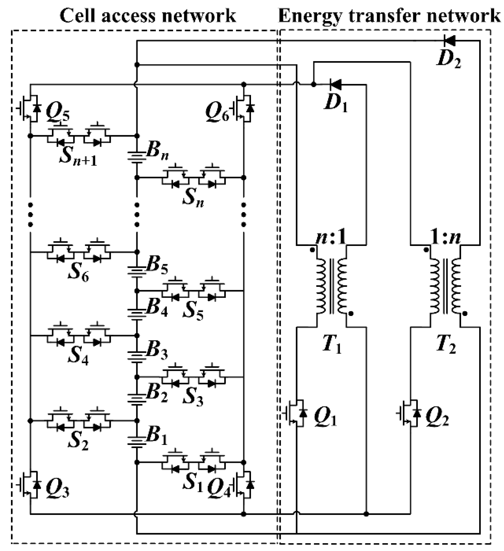
This paper presents a new active balancing circuit that uses double energy carriers. The proposed circuit simultaneously implements cell-to-pack and pack-to-cell balancing operations in the same switching period without overlapping. It can therefore effectively equalize batteries during charging and discharging conditions and can achieve fast balancing by using the high balancing power rate of double energy carriers. The structure and operation of the proposed active balancing circuit are proposed in
Section 2. Experimental results are presented in
Section 3. Discussion and comparison with other balancing circuits are given in
Section 4. The conclusion is given in
Section 5.
3. Experimental Results
The proposed balancing circuit simultaneously implements pack-to-cell and cell-to-pack balancing operations so the balancing powers of each operation are set as equal. The average balancing powers
Pb.avg1 from the battery pack to the weakest cell and
Pb.avg2 from the strongest cell to the battery pack are
where
D is the duty ratio of both
Q1 and
Q2. Assuming
nVBM =
VP and
Pb.avg1 =
Pb.avg2, the ratio of
Lm1 and
Lm2 can be set as
When the battery pack is charged or discharged using current
IP, the sum of the balancing current and
IP should not exceed the charging current limit (CCL) or the discharging current limit (DCL):
From (1), (2), and (8),
Lm1 and
Lm2 should be designed as
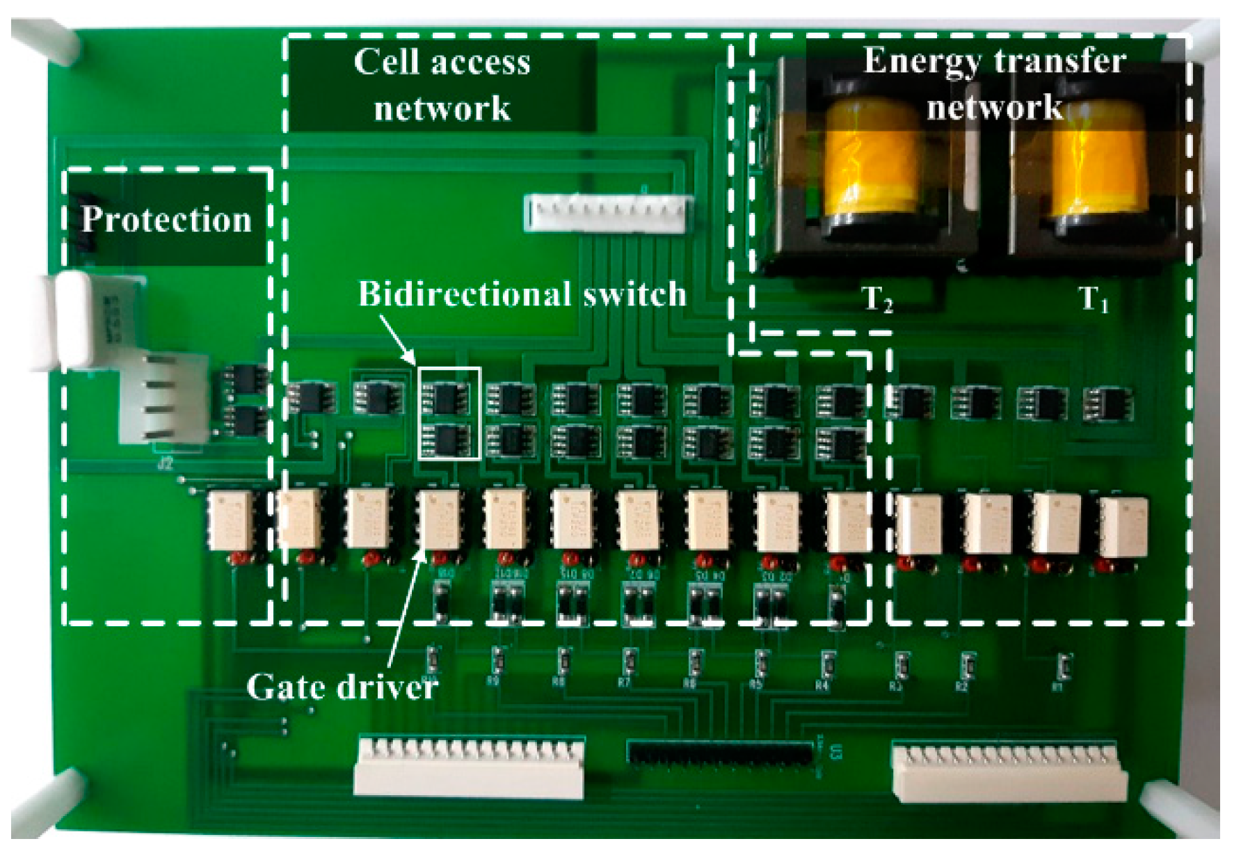
To verify the effectiveness of the proposed circuit, a prototype (
Figure 7) was fabricated and tested. The battery pack was composed of six serially-connected LIB cells (LG Chem., Ltd.) which had a nominal capacity of 4400 mA∙h. The battery pack had a nominal voltage of 21.6 V with CCL = 4.3 A and DCL = 6.45 A. The prototype had
fs = 40 kHz and
D = 0.5 and turns ratios 1:6 for
T1 and 6:1 for
T2, with designed values of
Lm1 = 1.45 mH and
Lm2 = 39.6 μH from (8) and (10). The switches and diodes were FDS3572 and FSV540 from On Semiconductor Co., Ltd. and the gate drivers were TLP250 from Toshiba Co., Ltd. The voltages of each cell were measured using a PXI-6254 data-acquisition board (National Instruments, Ltd.) and the gate signal for all switches was output by a PXI-6542 digital waveform generator (National Instruments, Ltd.).
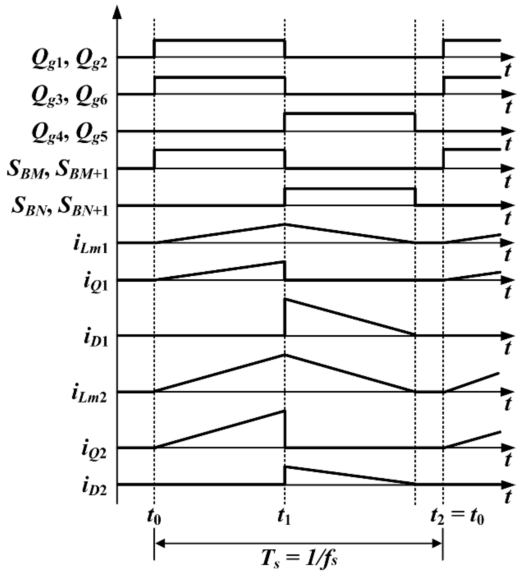
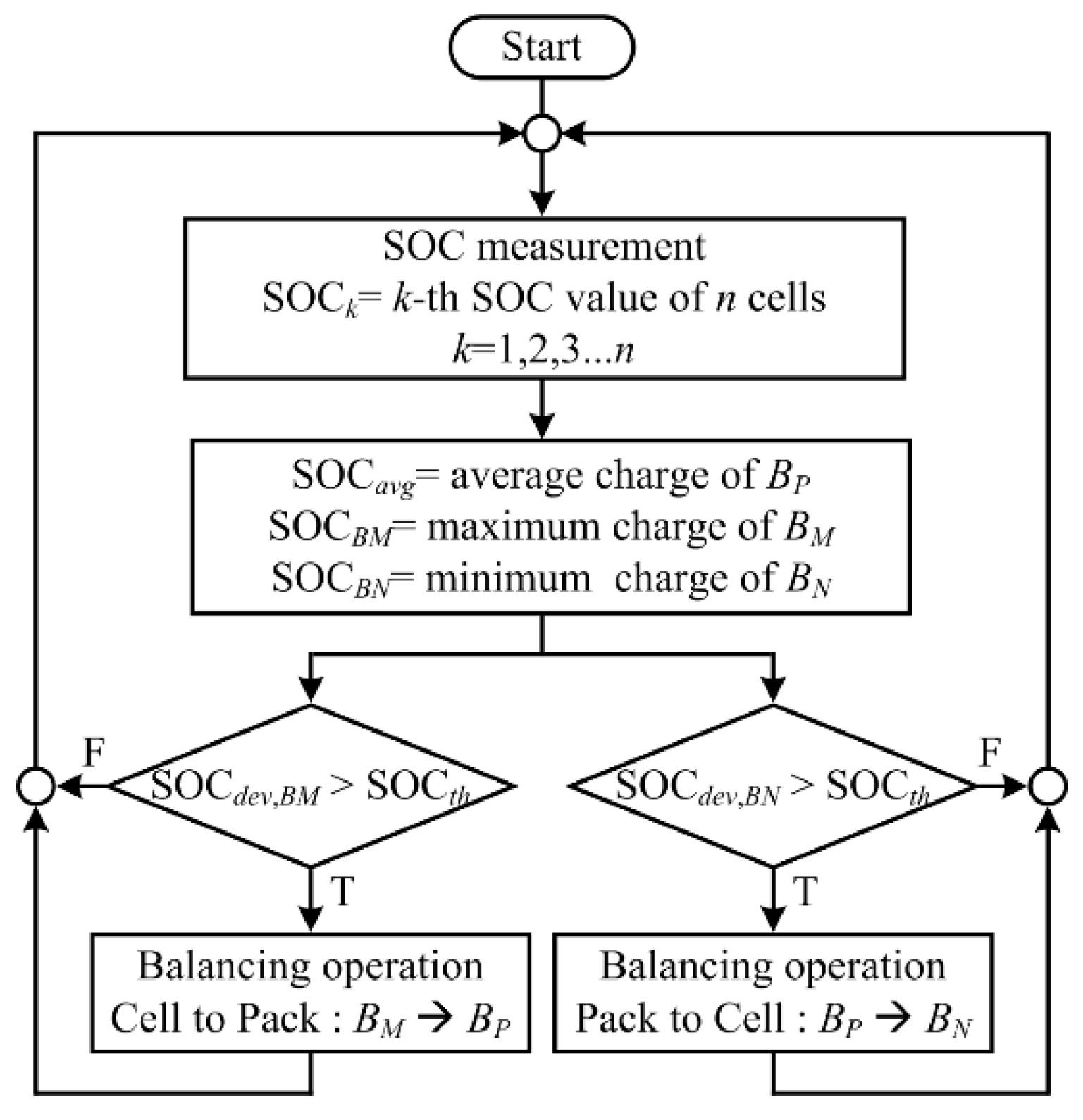
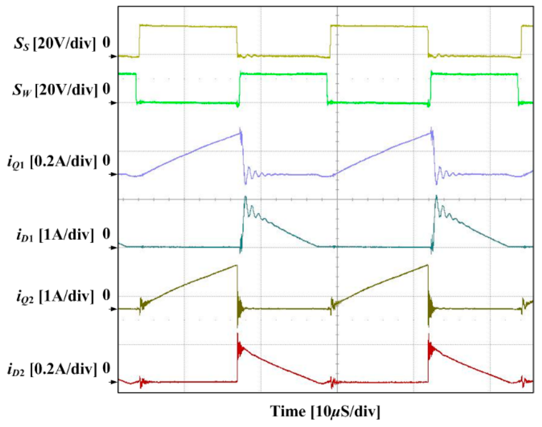
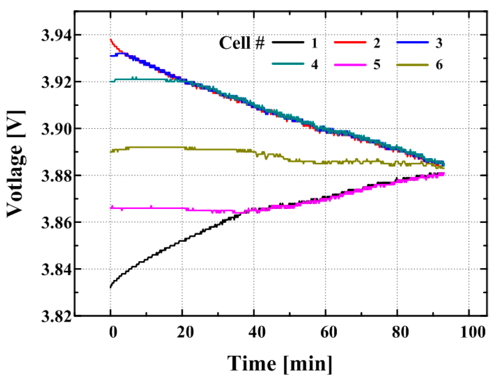
First, the six cells were balanced to prove the operation of the proposed balancing circuit and balancing algorithm. The voltage and current waveforms (
Figure 8) were measured using a 610Zi oscilloscope (Teledyne Co., Ltd.). The waveforms agreed well with the theoretical waveforms (
Figure 4). The initial SOC values of the six serially-connected cells were 69.94%, 79.24%, 79.19%, 78.17%, 73.18%, and 75.41%, and the cell numbers were assigned based on the order of series connection in the battery pack; the bottom-located cell was cell number 1 and the top-located cell was cell number 6. SOC
th was set to 0.2% and all cells converged to 3.883 ± 0.002 V (SOC = 74% ± 0.2%) after 93 min (
Figure 9). This experiment shows that the proposed balancing circuit provides good simultaneous implementation of cell-to-pack and pack-to-cell balancing operations.
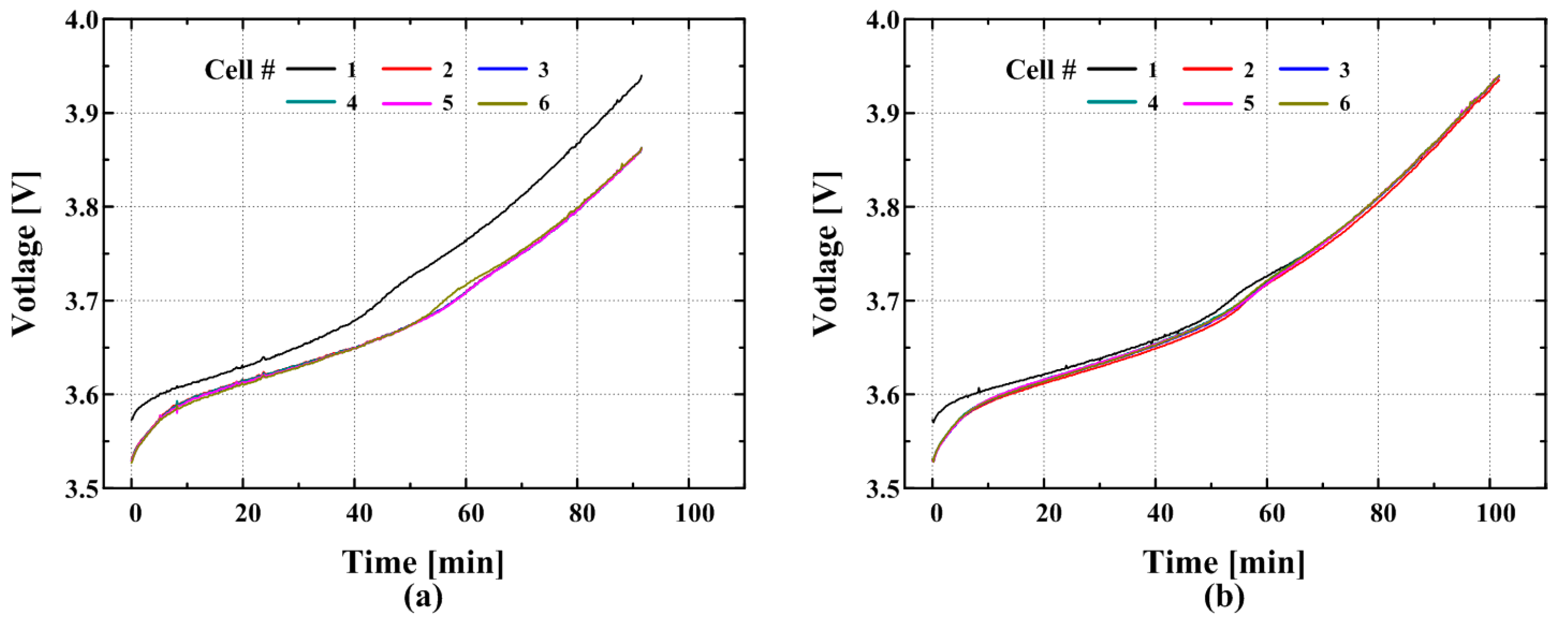
Second, the balancing operation of the strongest cell was measured within a charging operation (
Figure 10) and the speeds of only pack-to-cell and cell-to-pack balancing operations were compared. CVL was set to 3.94 V (SOC = 80%) and the battery pack had charging current
Ich = 1.5 A. The strongest cell (cell number 1) was set to 3.577 V (SOC = 30.64%) and the other five cells (cell numbers 2–5) were set to 3.53 V ± 0.01 V (SOC = 20.33% ± 0.02%). The strongest cell reached the CVL after 91.5 min in the pack-to-cell balancing operation (
Figure 10a) and after 101.66 min in the cell-to-pack balancing operation (
Figure 10b).
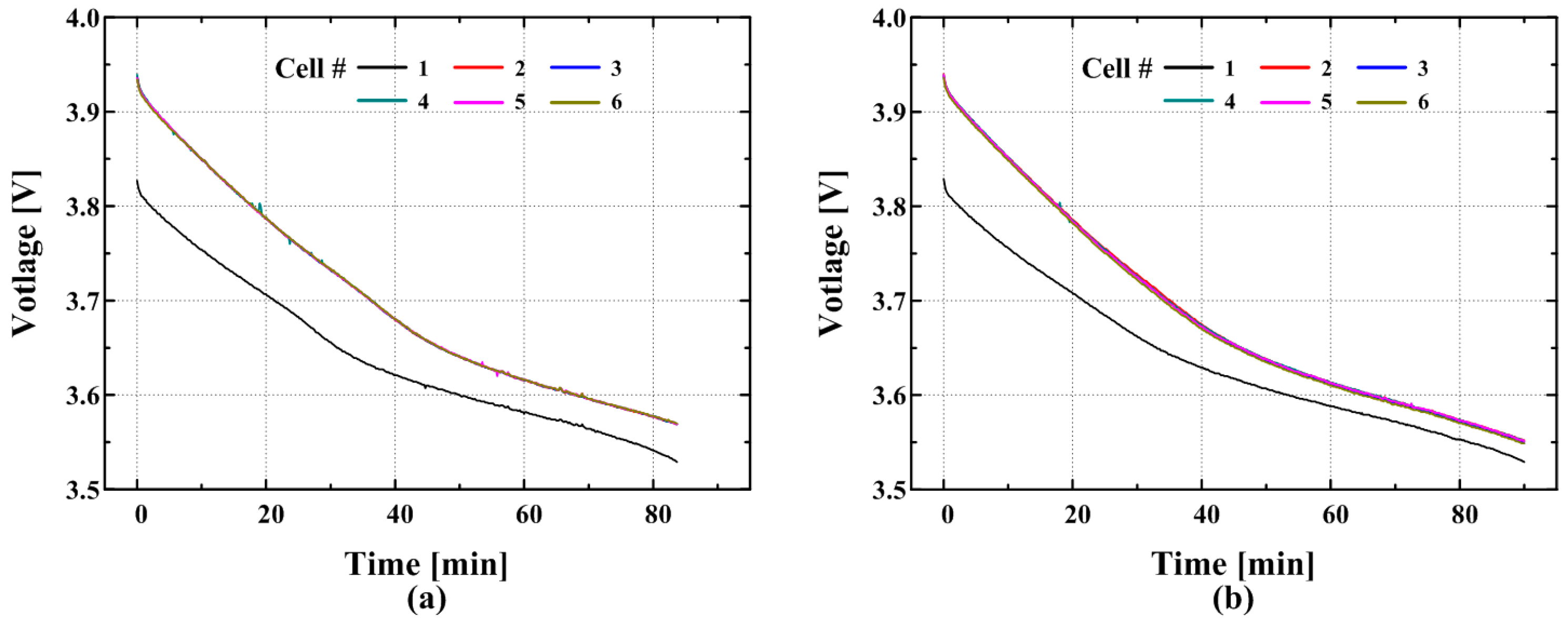
Third, the balancing operation of the weakest cell was implemented within a discharging operation (
Figure 11) and the speeds of both balancing operations were compared in the same manner. The DVL was set to 3.529 V (SOC = 20.21%) and the battery pack had a discharging current
Idis = 1.5 A. The weakest cell (cell number 1) was set to 3.829 V (SOC = 69.68%) and the other five cells (cell numbers 2–5) were set to 3.938 V ± 0.02 V (SOC = 79.81% ± 0.02%). The weakest cell reached the DVL after 83.66 min in the cell-to-pack balancing operation (
Figure 11a) and after 90 min in the pack-to-cell balancing operation (
Figure 11b).
These (
Figure 10 and
Figure 11) show that the cell-to-pack balancing operation has good speed in balancing the strongest cell during a charging operation and that the pack-to-cell balancing operation is suitable for balancing the weakest cell during a discharging operation. These results mean that a simultaneous balancing operation of the proposed circuit can be effectively used in both charging and discharging operations.
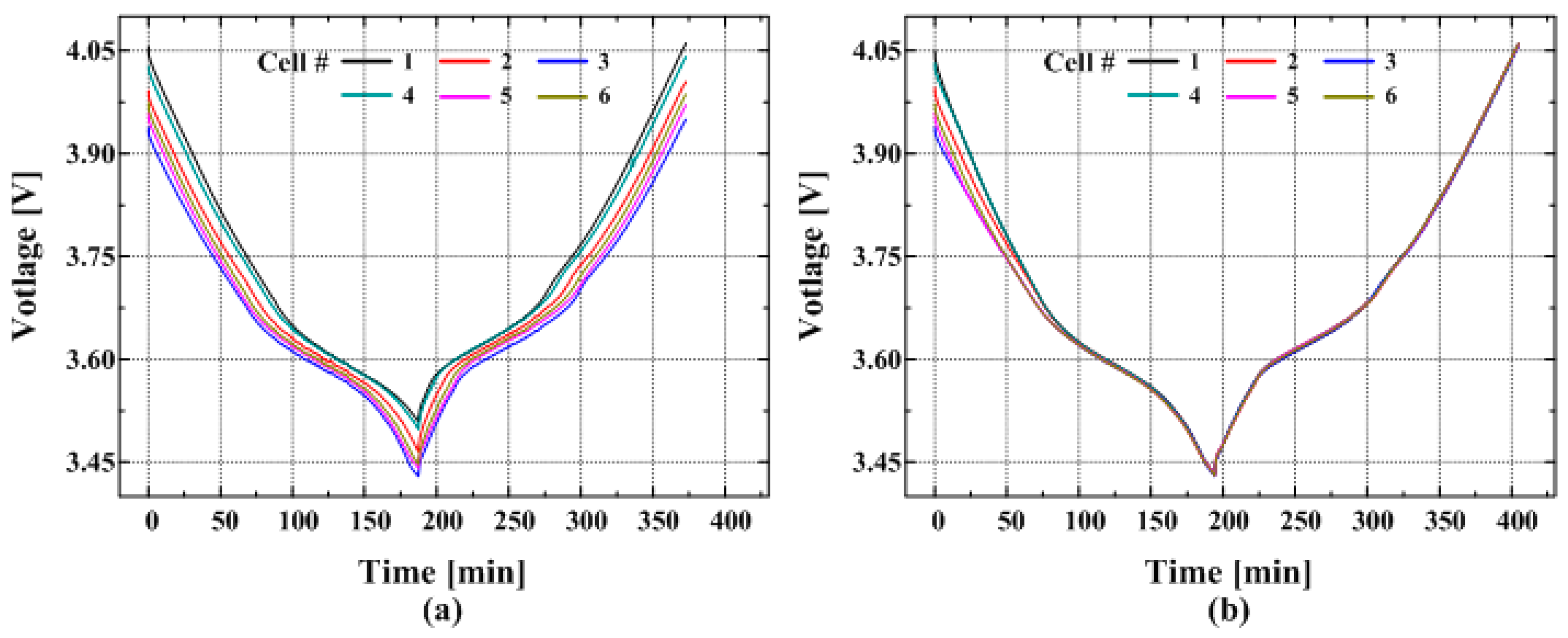
Finally, one charging/discharging period (
Ich =
Idis = 1A) between CVL = 4.061 V (SOC = 90.1%) and DVL = 3.429 V (SOC = 10.13%) was measured for a non-balancing operation and balancing operation (SOC
th = 0.2%) (
Figure 12). The initial SOCs were 89.22%, 84.89%, 79.92%, 87.8%, 81.78%, and 82.92%. During the discharging period, the weakest cell reached the DVL at 187.33 min in the non-balancing operation and at 194.16 min in the balancing operation. During the next charging period, the strongest cell reached the CVL at 372.83 min in the non-balancing operation and at 404.83 min in the balancing operation; i.e., one charging/discharging period in the balancing operation was increased by 32 min, which increased the capacity of battery pack by 8.58%. These results mean that a battery pack supported by the proposed balancing circuit can store more energy from the energy sources and supply more energy to the application of the battery pack.
4. Discussion
To display the advantages of the proposed circuit we have compared it with previous balancing circuits (
Table 2); the number of components in the balancing circuit and balancing performance, including control method and balancing speed, were evaluated under the assumption of
n cells per battery pack.
When the minimum balancing time was calculated, CCL = 4.3 A and DCL = 6.45 A at Ich = Idis = 0. In addition, a six serially-connected battery pack was assumed by using 4400 mA∙h Li-ion cells from LG-Chem, Ltd; the total charge Q of the cell was 15,840 C. The SOC values of six serially connected cells were assumed to be 47% (3.633 V, 7444.8 C), 48% (3.638 V, 7603.2 C), 49% (3.644 V, 7761.6 C), 51% (3.66 V, 8078.4 C), 52% (3.669 V, 8236.8 C), and 53% (3.679 V, 8395.2 C). The efficiency of balancing circuit was assumed to be 100%, so Qb = 7920 C (3.651 V, SOC = 50%).
The time shared flyback balancing circuit used in [
8] requires one transformer, 2
n − 1 diodes, and 2
n − 2 MOSFETs. The primary winding of the transformer is connected to the battery pack through the diode and the secondary winding is connected to a cell through the cell access network. The circuit measures all cell voltages and then sorts the cell voltages in ascending order. During the half switching period, the transformer sequentially collects the energy of each cell using the cell access network at a current < DCL, except for the weakest cell with the lowest cell voltage. The collected energy is released to the battery pack during the other half of the switching period at a current < DCL/
n. Since the energy collection from each cell depends on the cell voltage, the order of cell voltages must be verified for each switching period. This increases the complexity of the balancing algorithm and gate signal control. The time shared flyback balancing circuit only supports the cell-to-pack balancing operation, meaning the weakest cell (
Qweakest) determines the balancing time and the balancing operation is not efficient under the discharging conditions of the battery pack. Because this circuit uses the transformer as an energy carrier, DCL ≈ (2/
D) ∙
iB and
tB > 2
n∙(
Qb −
Qweakest)/(
D∙DCL), where
iB is the average balancing current. Thus, the calculated minimum balancing time is 1,105 s.
The half-bridge balancing circuit used in [
10] requires one multi-winding transformer, 4
n diodes, one inductor, two capacitors, and two MOSFETs. The primary winding of the multi-winding transformer is connected to the battery pack through the half bridge structure and the secondary windings are connected to the battery cells through the full bridge rectifiers. This circuit collects the energy of the battery pack during the half switching period at a current < CCL and releases this energy to the weakest cell during the other half switching period at a current < CCL/
n. When the collected energy is released to the weakest cell, the secondary windings are clamped to the cell voltage of the weakest cell. All rectifiers except the weakest cell are off and the balancing energy is delivered only to the weakest cell. The half-bridge balancing circuit does not require cell voltage detection and the balancing algorithm is very simple. The switches operate in fixed duty. Therefore, the circuit is very easy to control. However, since the circuit only supports the pack-to-cell balancing operation, the strongest cell (
Qstrongest) determines the balancing time and the balancing operation is not efficient under the charging condition of the battery pack. Because the circuit uses the transformer as an energy carrier, CCL ≈ (2/
D)∙
iB and
tB > 2
n∙(
Qstrongest −
Qb)/(
D∙CCL); the calculated minimum balancing time is 1,657 s. The half-bridge balancing circuit requires one multi-winding transformer and many diodes, which are the main hurdles to implementing a balancing circuit for high capacity battery packs.
The switched capacitor circuit used in [
15] requires
n capacitors and 2
n + 4 MOSFETs. Unlike the conventional switched-capacitor circuit of [
13], this circuit adds an auxiliary capacitor (
CA) and switches to allow energy transfer between the top cell and the bottom cell, meaning it has a faster balancing speed than a conventional circuit. The balancing energy is transferred by shunting the capacitor from one cell to another adjacent cell alternately; it does not require cell voltage detection. The balancing algorithm is very simple, but the balancing speed is slow when the cell-voltage difference between adjacent cells is small. In this circuit, the capacitor
C collects energy when the capacitor voltage
Vcap is lower than the cell voltage
Vcell. Otherwise, the capacitor releases energy to the cell; the amount of charge transferred for one switching operation is
. Because the total deviation of the
i-th cell charges
Qi from
Qb is
, the amount of charge transferred by the circuit per each switching operation is
, where
Vcell(i) is the voltage value of
i-th cell,
Vcap(i,i+1) is the voltage value of capacitor
C(i,i+1), which is located between
i-th cell and (
i + 1)-th cell, and
Vcap(A) is the voltage value of
CA. This circuit transfer
Qt,n totals
N =
tB/
Ts times during the balancing operation of
tB, meaning the total transferred balancing charge
, where
Vcell(i),initial is initial voltage of the
i-th cell and
Vcap(i,i+1),final and
Vcap(A),final are the final voltages of
C(i,i+1) and
CA, respectively. Finally, these factors determine
tB as
and
; the calculated minimum balancing time was 28,586 s at
C(i,i+1) =
CA = 25 μF,
Ts = 25 μs, and
Vcap(i,i+1),final =
Vcap(A),final ≈ 3.651 V.
The LC resonant balancing circuit used in [
18] requires one inductor, one capacitor, and 2
n + 10 MOSETs. This circuit transfers the balancing energy using the LC resonance, so all MOSFETs operate with ZCS. In addition, it can achieve a fast balancing speed in a large-scaled battery pack because it directly transfers the collected energy from the strongest cell to the weakest cell. Because this circuit uses an LC resonant circuit as an energy carrier, DCL ≈ π∙
iB and the deviation of cell charges
Qi from
Qb,
, determines
tB as
. Thus, the calculated minimum balancing time is 694 s. However, this circuit requires a complex zero-current detection circuit for the control of the gate signal and initializing circuit for the gate driver. In addition, it requires a complex procedure to generate the gate signals, taking into account the target charge states, the SOCs of all cells, the efficiency of the balancing circuit, and the average balancing power.
The buck-boost balancing circuit used in [
20] requires one multi-winding transformer and 2
n MOSFETs. Compared to the buck-boost balancing circuit used in [
16], this circuit uses a multi-winding transformer to reduce the number of inductors and to extend the energy transfer range. In the circuit used in [
16], the energy transfer is possible only between adjacent cells, but energy transfer between all cells of the battery pack is possible in the circuit used in [
20]. Since energy transfer from the strongest cell to the weakest cell is possible, the circuit used in [
20] can achieve a fast balancing speed. Because this circuit uses the transformer as an energy carrier, CCL ≈ (2/
D)∙
iB and the deviation of cell charges
Qi from
Qb,
, determines
tB as
for
D = 0.5; the calculated minimum balancing time is 884 s. The fabrication of a multi-winding transformer is a major hurdle to implementing a balancing circuit for high capacity battery packs. The circuit used in [
20] examines the parity between the strongest and weakest cells and works differently for three different parity conditions. Case 1: The circuit operates as a buck-boost converter when the balancing energy is transferred from an odd-numbered cell to an adjacent even-numbered cell. Case 2: The circuit operates as a flyback converter when the balancing energy is transferred from a nonadjacent odd-numbered cell to an even-numbered cell. Case 3: When the balancing energy is transferred between same parity cells, the circuit works like a buck-boost converter to collect the balancing energy and like a fly-back converter to release the collected energy. Thus, the circuit used in [
20] requires a very complicated control algorithm.
Compared to the previous balancing circuits, the proposed circuit requires only two transformers, two diodes, and 2
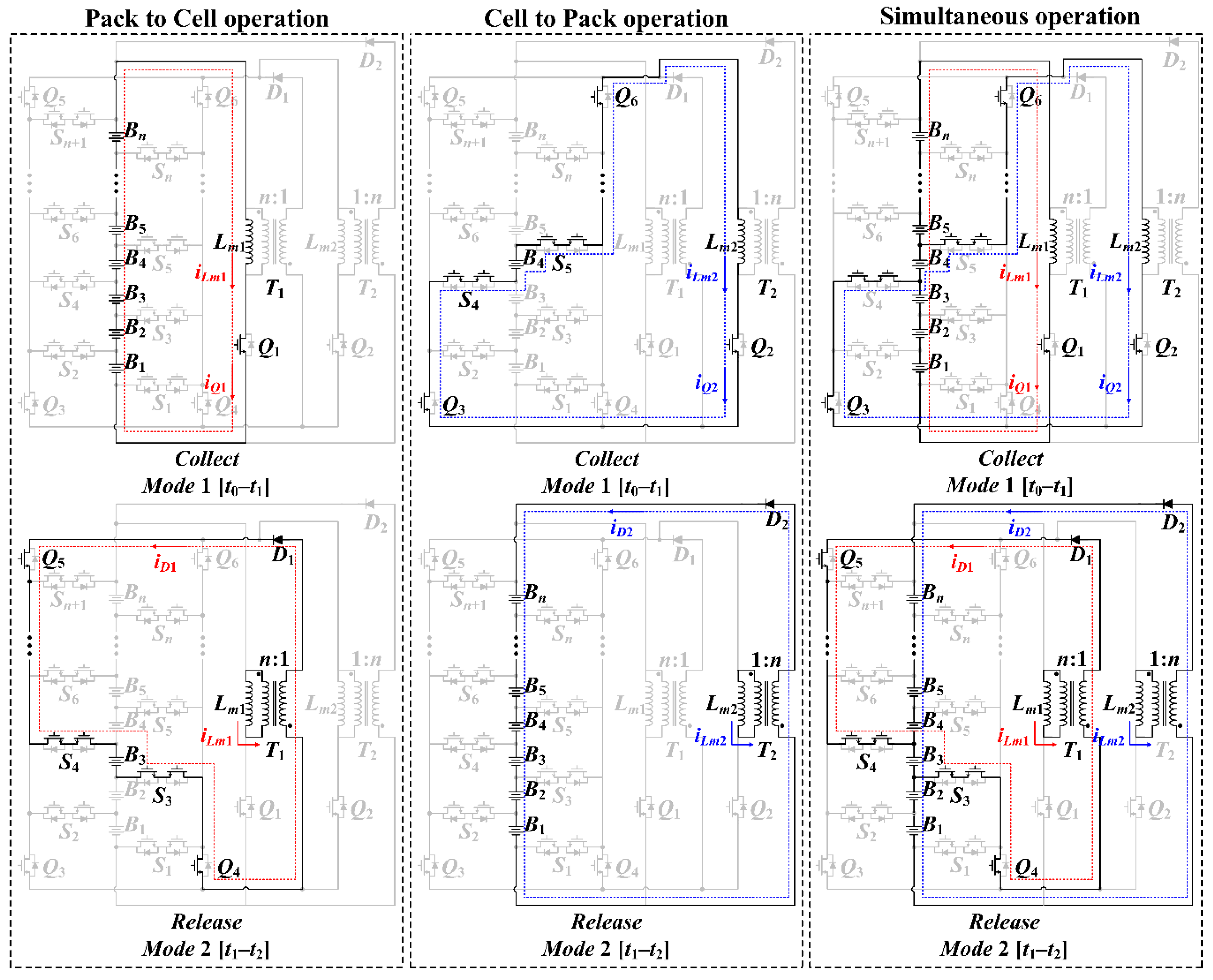
n + 8 MOSFETs. The proposed circuit allows both pack-to-cell and cell-to-pack balancing operations to be used at the same time and requires only two operation modes: the collect mode and the release mode (
Figure 3 and
Figure 4). The proposed circuit works like a flyback converter for all parity conditions in the strongest and weakest cells and has a faster balancing speed than the circuits used in [
18,
20]. The proposed circuit collects the energy from strongest cell with
iB ≈ (
D/2)∙DCL and releases the collected energy to the weakest cell with
iB ≈ (
D/2)∙CCL. Thus,
tB is determined as
for CCL < DCL and
D = 0.8; the calculated minimum balancing time is 552 s, which is the fastest time when compared with other methods. The balancing speed was improved by using double energy carriers and by increasing the switching duty
D.


