Article

Series-Series/Series Compensated Inductive Power Transmission System with Symmetrical Half-Bridge Resonant Converter: Design, Analysis, and Experimental Assessment

1
Department of Instrumental and Electrical Engineering, Xiamen University, Xiamen 361005, China
2
Fujian Collaborative Innovation Center for R&D of Coach and Special Vehicle, Xiamen 361024, China
*
Author to whom correspondence should be addressed.
Energies 2019, 12(12), 2268; https://doi.org/10.3390/en12122268
Submission received: 24 April 2019 / Revised: 3 June 2019 / Accepted: 8 June 2019 / Published: 13 June 2019

Abstract

:
In order to compensate the large leakage inductance and improve the power transmission capacity, capacitors are widely used in inductive power transfer (IPT) systems, which results in high voltage or current stresses in the resonant tanks and limits higher volt-ampere (VA) rating of the transfer power, especially in medium and low frequency applications. This paper presents a symmetrical half-bridge resonant converter (SHRC) for series-series/series compensated IPT systems with detailed analysis and design. It operates at a relatively low frequency of 12.5 kHz, suitable for IGBT applications. The theoretical analysis shows that, compared with full-bridge resonant converter (FRC) for IPT, the symmetrical half-bridge resonant converter achieves a higher efficiency. Simulation and a prototype of 1500 W power output were built to verify the theoretical analysis. The experimental results show that the power loss of SHRC is 39.7 W while that of FRC is 79.4 W, which is consistent with the theoretical analysis. The global efficiency of the IPT based on the proposed converter is 91.6%.

1. Introduction

Inductive power transfer (IPT) systems transfer electric power across an air gap by magnetic coupling and produces comparative advantages over transfer with physical contact. It has been widely used in commercial and industrial applications where convenience and safety are imperative, such as household apparatuses [1], biomedical applications [2], and electric vehicle (EV) charging [3,4,5,6,7,8,9]. Different from strongly coupled systems, the mutual coupling of IPT systems is generally weak. The leakage inductance is relatively high, and the coupling coefficient k is usually less than 0.2, resulting in a large reactive power which can be up to 50 times the transmitted power [10]. Moreover, system losses increase due to high reactive current [11]. To deliver the required power, improve the transfer efficiency, and minimize the VA rating of the power supply, it is necessary to compensate the leakage inductance [11,12]. Four basic compensation topologies, which are series/series (S/S), series/parallel (S/P), parallel/series (P/S), and parallel/parallel (P/P), were widely used in a number of studies [10,11]. The primary parallel compensation topologies (P/S and P/P) are fed by current source or with a bulky inductor [4,13,14,15], while the primary series topologies (S/S and S/P) are fed by voltage source [16]. Compared with P/S and P/P topologies, S/S and S/P topologies which require less space are more commonly used in IPT [4,17]. Compared with S/P topology, S/S compensation can achieve better overall efficiency [18], requires less copper mass [3], and is independent of the load [19]. Our research in this paper based on the S/S topology.
Derived from the four basic compensation topologies, more compensation topologies were proposed to improve the IPT systems. An SP/S compensation method, which can be regarded as a combination of S/S and P/S, was used to achieve a high misalignment tolerance without adjusting the primary power supply [20]. S/SP compensation topology was proposed to achieve high efficiency and good output controllability [12]. LCL compensation topology with two large inductors was presented to avoid instantaneous changes in the voltages of the inverter and was proved to be suitable under variations of load and coupling coefficient [21]. In order to reduce the size of the inductors in LCL, LCC was proposed in [22], which had high misalignment tolerance and load independence characteristics [15]. LCC was further optimized to suitable for EVs charging in [7]. An efficient double-sided LCC for IPT system was proposed in [23], and the dead time optimization of this double-sided LCC topology for power and efficiency enhancement were further studied in [24]. However, the compensation networks became more complex with additional capacitors and/or inductors. The orders and interdependency of the IPT system increased. The combination of inductor and/or capacitor of the four basic compensation topologies is rarely studied.
In a strongly coupled transformer system, the full-bridge topology is widely used rather than half-bridge topology. The reasons are probably related to the following issues of the half-bridge topology: Poor controllability, low power density, and voltage imbalance of the two capacitors. However, in the IPT systems the shortages of half-bridge topology become less important. The main factor limiting the power capacity of the IPT system is the high voltage stresses of the compensated capacitors due to the large leakage inductance, especially when the operating frequency is relatively low. On the other hand, the half-bridge topology has advantages such as less power devices and lower cost. In this paper, a series-series/series (SS/S) compensated symmetrical half bridge resonant converter (SHRC) with double capacitors in primary is presented as shown in Figure 1a. Without increasing the order of the system, the system characteristics and efficiency of the proposed topology will be discussed by comparing with the full-bridge resonant converter (FRC)-based IPT system as shown in Figure 1b. In order to make the converter smaller with smaller filter capacitor, three-phase AC power sources with rectifier and filter are adopted in both Figure 1a,b.
The main contents of this paper are organized as follows: The detailed design process is analyzed in Section 2. The efficiency analysis of the proposed system and an efficiency comparison between SHRC and FRC are shown in Section 3. Simulations and experimental results are given in Section 4 to verify the analysis. Finally, Section 5 contains the conclusions and discussions.

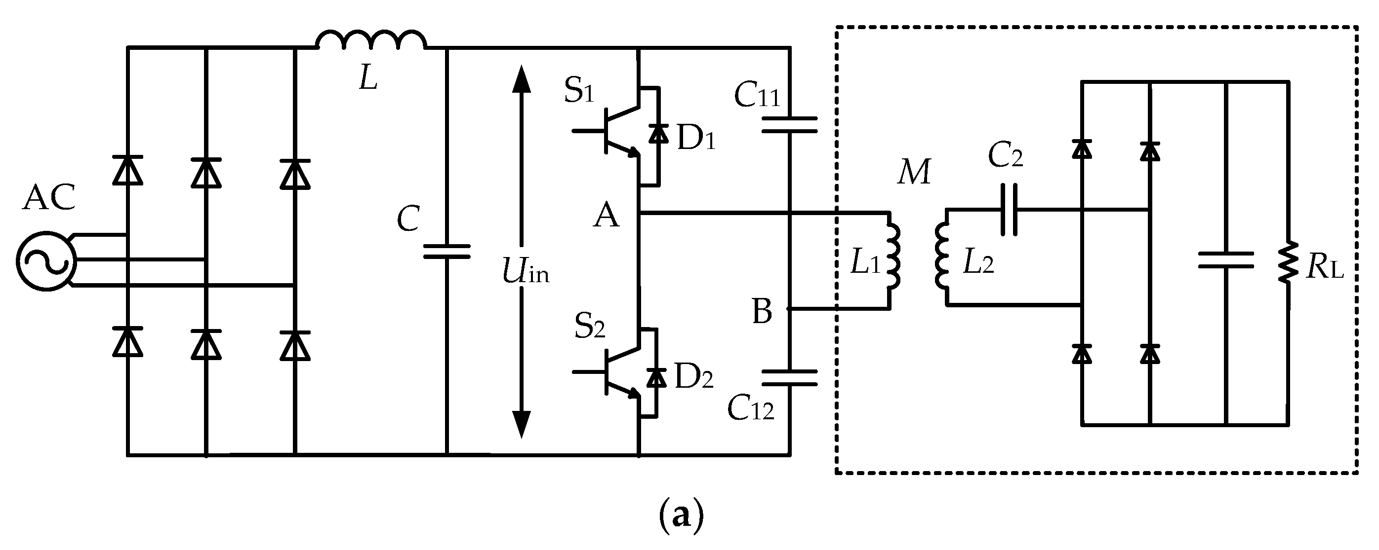
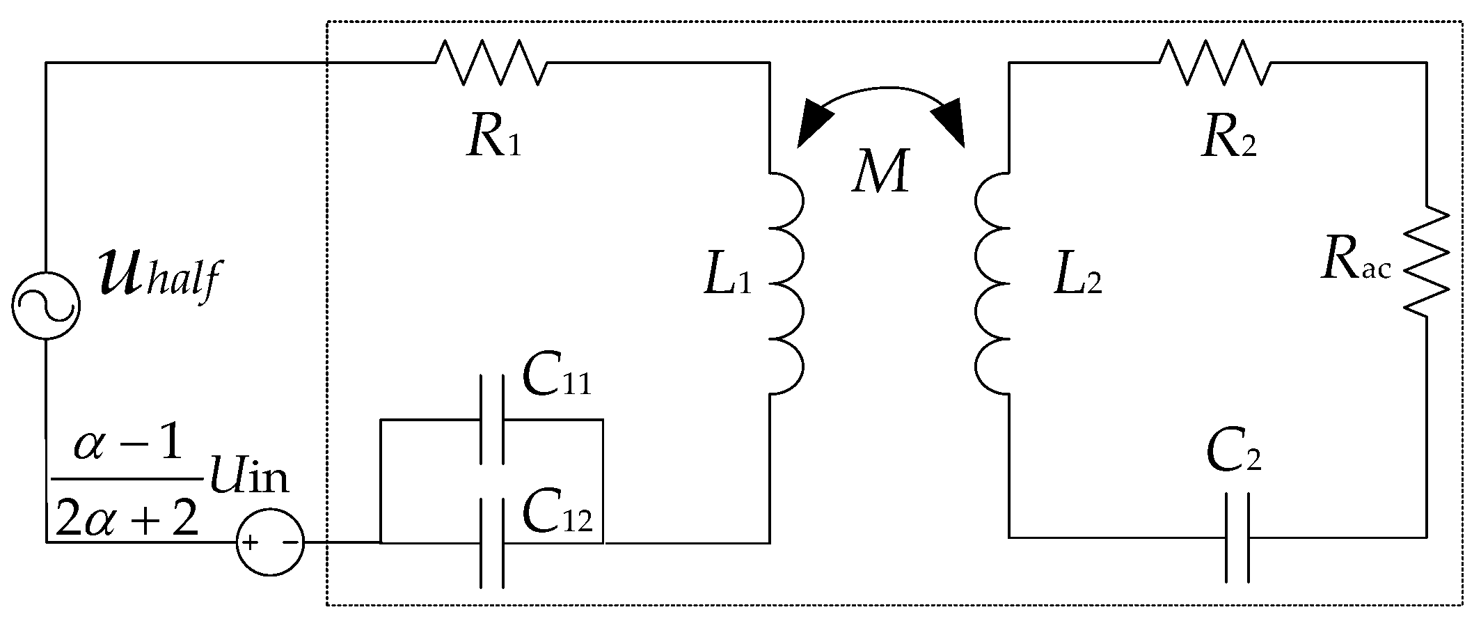
2. Proposed Topology and Operation Analysis
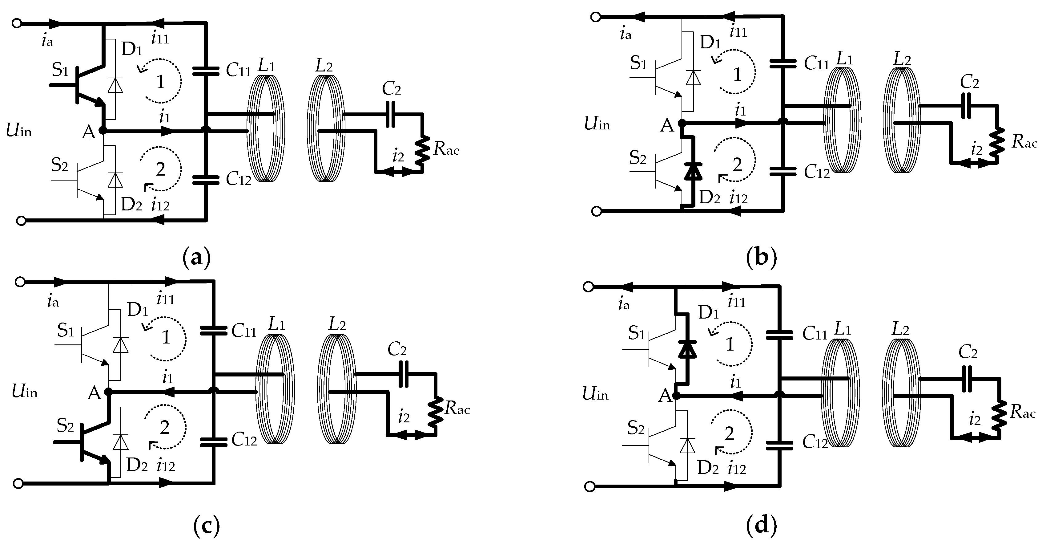
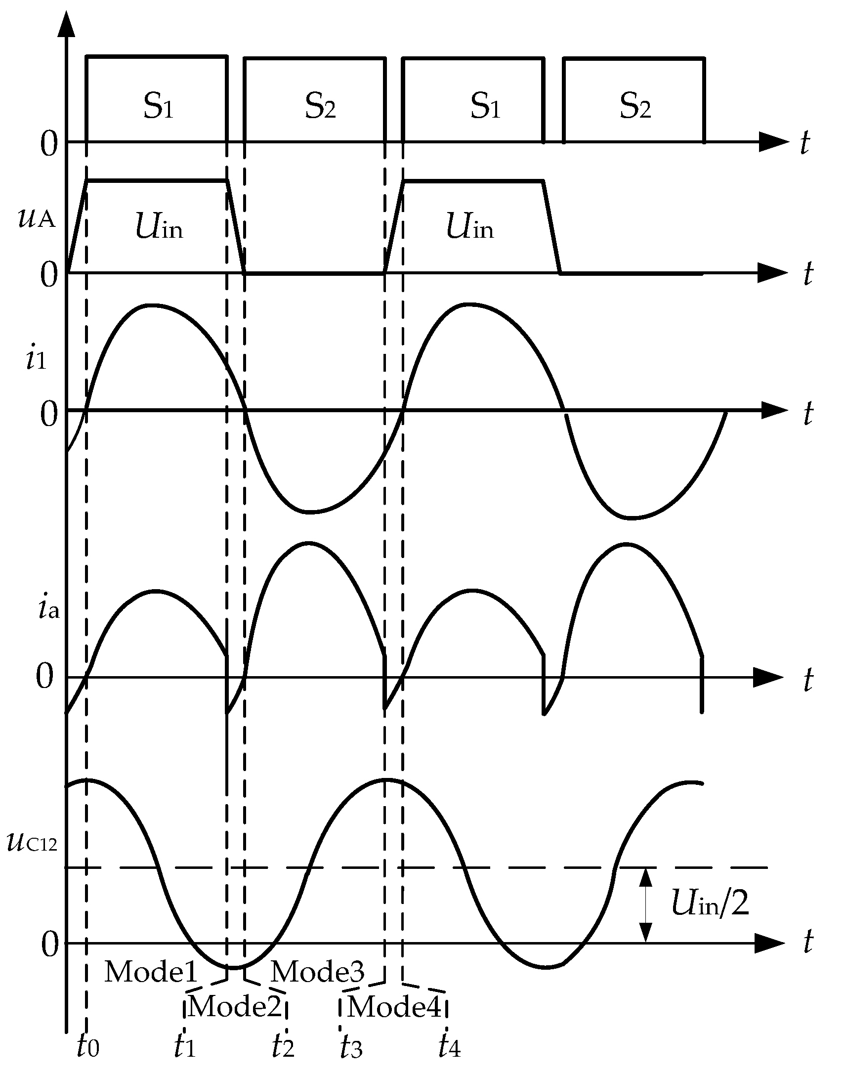
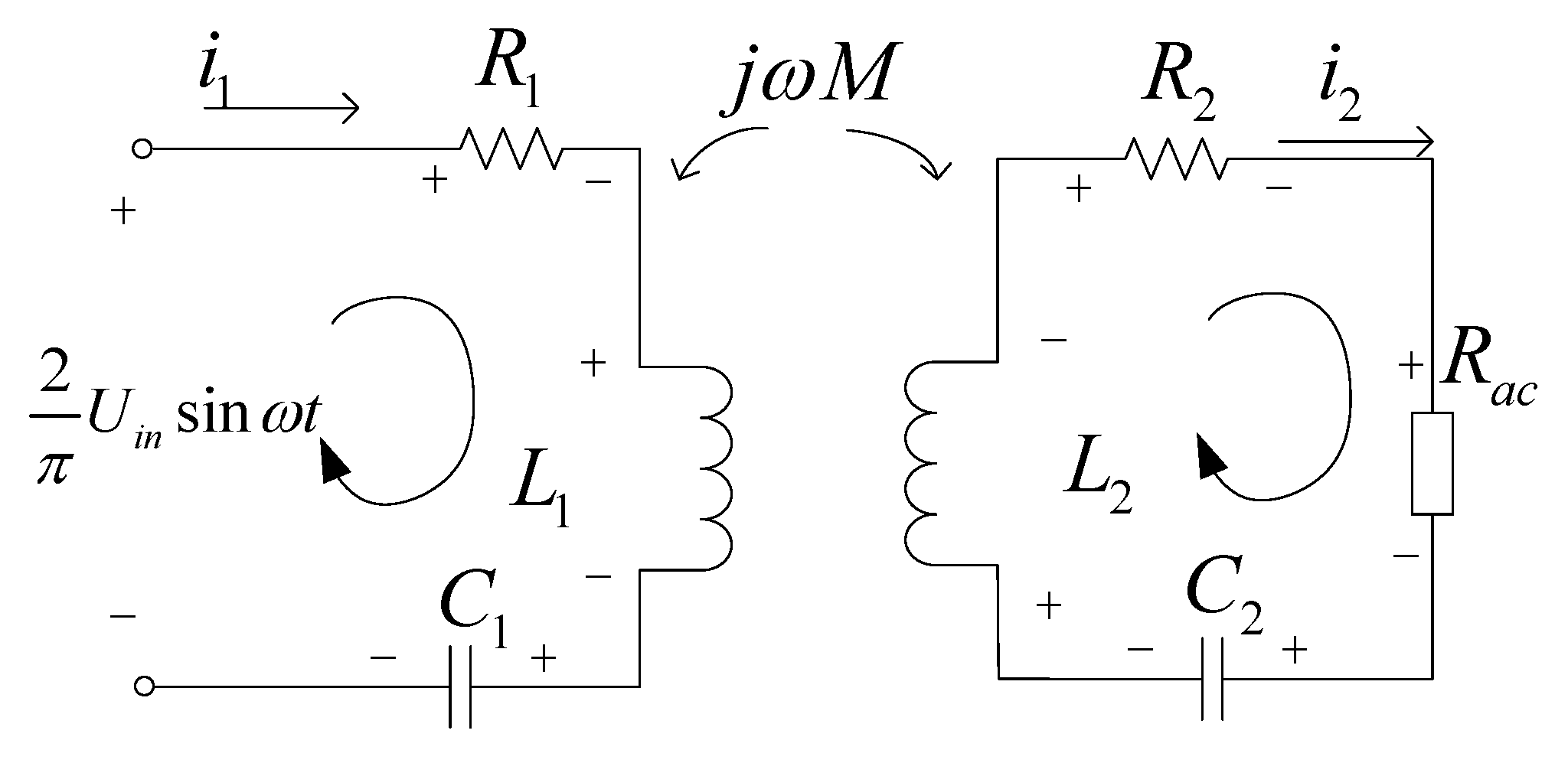
The topology of the SS/S SHRC is shown in Figure 1a. Different from the traditional half-bridge converter, the voltage value of point B is varying instead of Uin/2. C11 and C12 are the primary compensation capacitors, which are in series with the inductor and connected to the DC power Uin. The capacitance of the two capacitors are not necessarily the same, and one can be zero. The secondary is series compensated. To achieve optimal efficiency, the IPT system operates in resonance [13]. Interestingly, converter fed by voltage source for IPT generally operates in near resonance frequency with slightly inductive in practical applications.

2.1. Mode Analysis

In Figure 1a, S1 and S2 alternatively turn on converting DC source Uin into high-frequency AC power to drive the resonant circuit. The primary resonant circuit consists of capacitor C11, C12, and coil L1. Coils of primary L1 and secondary L2 have the same structure. There are four operational modes of the proposed topology as shown in Figure 2. The main waveforms of these modes are illustrated in Figure 3 where i1 is the current of the primary inductor, ia is the input current, uA is the voltage of point A, and uC12 is the voltage of capacitor C12.
Mode 1 [t0, t1]: Before t0, switch S1 is off. The input current ia flows through antiparallel diode D1. Therefore, at t0, S1 turns on under zero-current-switching (ZCS) and zero-voltage-switching (ZVS) conditions. During this mode, S1 turns on, input voltage Uin is connected to the primary resonant circuit as Figure 2a. Taking into account of conduction loss of switch, system dynamics is given by
{ ( r L + r C + r o n ) i 1 + j ω L 1 i 1 + i 11 j ω C 11 + j ω M i 2 = 0           loop 1 ( r L + r C + r o n ) i 1 + j ω L 1 i 1 + i 12 j ω C 12 + j ω M i 2 = U in         loop 2
where
i 11 + i 12 = i 1
ron, rL, and rC are the equivalent on-resistance of the switch, lumped resistance of primary coil, and equivalent series resistance of resonant capacitor, respectively. i11 and i12 are the current of C11 and C12, respectively. When
C 12 = α C 11
C 1 = C 11 + C 12 = ( 1 + α ) C 11
and based on Equation (2), Equation (1) is simplified as Equation (5) by adding the left side of loop 1 to the left side of loop 2 and adding the right side of loop 1 to the right side of loop 2.
( r L + r C + r o n ) i 1 + j ω L 1 i 1 + i 1 j ω C 1 + j ω M i 2 = α α + 1 U in
Mode 2 [t1, t2]: At t1, S1 turns off and the primary coil current i1 is low, but positive, and almost equal to 0. i1 keeps flowing into antiparallel diode D2, which insures ZCS and ZVS of S2 in mode 3. This mode also plays the role of dead zone for the converter. Simplified as mode 1, mode 2 system dynamics can be expressed as
U D + ( r L + r C ) i 1 + j ω L 1 i 1 + i 1 j ω C 1 + j ω M i 2 = 1 α + 1 U in
where UD is the turn-on voltage of antiparallel diode.
Mode 3 [t2, t3] and mode 4 [t3, t4] are similar to mode 1 and mode 2, respectively. The corresponding system dynamics are given by
( r L + r C + r o n ) i 1 + j ω L 1 i 1 + i 1 j ω C 1 + j ω M i 2 = 1 α + 1 U in
U D + ( r L + r C ) i 1 + j ω L 1 i 1 + i 1 j ω C 1 + j ω M i 2 = α α + 1 U in
To simplify the calculation, mode 2 and mode 4 can be represented by mode 3 and mode 1 since they are so short compared with mode 1 or mode 2. From the four mode system dynamics Equations (5)–(8), SHRC system dynamics are further simplified as
{ ( r L + r C + r o n ) i 1 + j ω L 1 i 1 + i 1 j ω C 1 + j ω M i 2 = α 1 2 α + 2 U i n + 1 2 U in        0 t < T 2 ( r L + r C + r o n ) i 1 + j ω L 1 i 1 + i 1 j ω C 1 + j ω M i 2 = α 1 2 α + 2 U i n 1 2 U in        T 2 t < T
where T is switching period of the converter. Equation (9) can be expressed as
( r L + r C + r o n ) i 1 + j ω L 1 i 1 + i 1 j ω C 1 + j ω M i 2 = α 1 2 α + 2 U in + u h a l f
where uhalf is a square wave with amplitude of Uin/2 and mean of 0. According to Equation (10), the SHRC systems can be presented as Figure 4.
Where
{ R 1 = r L + r C + r o n R 2 = r L + r C
If α = 1, DC component of Equation (10) α 1 2 α + 2 U in = 0 , the SHRC and FRC will share the same equivalent circuit as shown in the dotted rectangle in Figure 4. If α ≠ 1, based on first harmonic approximation method, Equation (10) can be simplified as Equation (12), Figure 4 can be presented as Figure 5, which is the same as α = 1 condition.
R 1 i 1 + j ω L 1 i 1 + i 1 j ω C 1 + j ω M i 2 = 2 π U in sin ω t
R a c = 8 π 2 R L
According to Kirchhoff’s voltage law (KVL), the system dynamics of secondary is given by
R 2 i 2 + R a c i 2 + j ω L 2 i 2 + i 2 j ω C 2 + j ω M i 1 = 0
By grouping Equations (12) and (14), the system dynamics of SS/S SHRC are present as
{ R 1 i 1 + j ω L 1 i 1 + i 1 j ω C 1 + j ω M i 2 = 2 π U in sin ω t R 2 i 2 + R a c i 2 + j ω L 2 i 2 + i 2 j ω C 2 + j ω M i 1 = 0
The input impedance of the primary impedance Z1, the secondary impedance Z2 and the reflected impedance Zr are given by
{ Z 1 = R 1 + Z r + j ω L 1 + 1 j ω C 1 Z 2 = R 2 + j ω L 2 + 1 j ω C 2 + R a c Z r = ω 2 M 2 Z 2
Equation (16) can be solved as
{ Z 1 = R 1 + ω 4 M 2 C 2 2 ( R 2 + R a c ) ω 2 C 2 2 ( R 2 + R a c ) 2 + ( ω 2 L 2 C 2 1 ) 2 j ( ( ω 2 L 2 C 2 1 ) ω 3 M 2 C 2 ω 2 C 2 2 ( R 2 + R a c ) 2 + ( ω 2 L 2 C 2 1 ) 2 + ω L 1 1 ω C 1 ) Z 2 = R 2 + R a c + j ( ω L 2 1 ω C 2 ) Z r = ω 4 M 2 C 2 2 ( R 2 + R a c ) ω 2 C 2 2 ( R 2 + R a c ) 2 + ( ω 2 L 2 C 2 1 ) 2 j ( ω 2 L 2 C 2 1 ) ω 3 M 2 C 2 ω 2 C 2 2 ( r 2 + R a c ) 2 + ( ω 2 L 2 C 2 1 ) 2
Z1, Z2, and Zr in Equation (17) are normalized as Z1n (Z1n = Z1/Z0), Z2n (Z2n = Z2/Z0), and Zrn (Zrn = Zr/Z0), respectively. The normalized impedance Z1n, Z2n, and Z2n as a function of the normalized angular frequency ωn (ωn = ω/ω0) and the normalized load resistance Rn (Rn = Rac/Z0) at k = 0.29 are further illustrated in Figure 6a–c, respectively. Where
Z 0 = L 1 C 11 + C 12
ω 0 = 1 L 1 ( C 11 + C 12 ) = 1 L 2 C 2
From Figure 6b,c, Z2n has a minimum value at the resonance frequency ω = ω0, while Zrn is the largest. In order to analyze Z1n, Figure 6d describes the trend of Z1n as a function of ωn using a two-dimensional graph. It is shown in Figure 6a,d that the maximum transfer power, when Z1n is the smallest, does not necessarily occur at the resonant frequency. When Rn > 0.5, maximum transfer power point is at the resonant frequency, while that of Rn = 0.2 or 0.25 is not. The frequency of the maximum transfer power bifurcates.
In order to make the IPT system operate at slightly inductive region which can be considered as resonance, it is necessary to analyze impedance angle of Z1. The impedance angle curve of the system is constructed by Equation (17), as shown in Figure 7. The resonant frequency bifurcation, which means there is more than one frequency where the angle of Z1 is zero, may occur when, for example, Rn < 0.3. Furthermore, when ω is in the near region of ω0, the impedance of the converter is capacitive when ω > ω0 and it is inductive when ω < ω0, which are contrary to a typical transformer system. This paper will use Rn = 0.25 as one of the design parameters to further prove the frequency bifurcation phenomenon, a frequency slightly lower than ω0 was chosen as ω to make it operate at slightly inductive region.

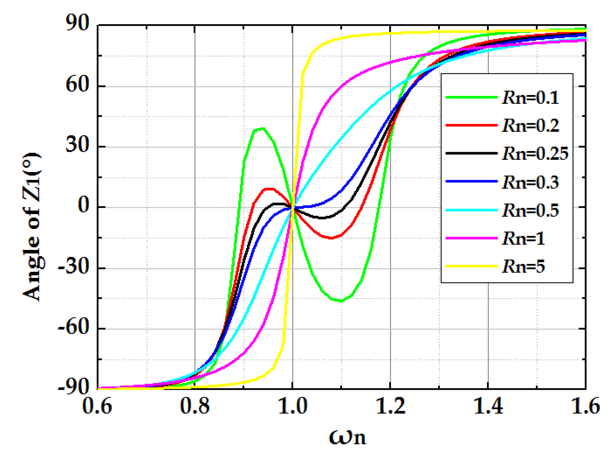
2.2. Resonance Analysis

When system operates in resonance, the imaginary part of Z1 is equal to zero. From Equation (17), the resonant frequency can be solved as
f 0 = ω 0 2 π = 1 2 π L 1 ( C 11 + C 12 ) = 1 2 π L 2 C 2
Equation (20) presents the relationship between L1, C11, C12, L2, and C2. When the designed resonant frequency is determined and coil structure is fixed, L1, L2 and f0 are determined. In order to ensure the resonance state of the system, the values of C11, C12, and C2 can be determined. The equivalent impedance of the secondary reflected to the primary is purely resistive. It can be seen from the Figure 7 and Equation (17) that, for different loads, the imaginary part of reflection impedance Zr is zero. Thus the resonance state of IPT system is load-independent.
Re ( Z r ) = ω 0 2 M 2 R 2 + R a c
Im ( Z r ) = 0
The primary input impedance is simplified as
Z 1 = R 1 + ω 0 2 M 2 R 2 + R a c
i 1 = 2 π U in sin ω t R 1 + ω 0 2 M 2 R 2 + R a c
The output power Pout can be calculated as
P o u t = ( 2 π ω 0 M U in sin ω t R 1 ( R 2 + R a c ) + ω 0 2 M 2 ) 2 R a c
From Equations (15)–(25) and the equivalent circuit as shown in Figure 5 and analysis in references [6,7,8,23], the proposed SS/S SHRC has the same characteristics as the FRC based on SS compensation topology. Capacitors C11 and C12, in series with the primary inductor L1, play the same role as the primary compensation capacitor in full-bridge topology. Capacitance of the dual capacitors is equal to C11 + C12 as shown in Equation (4). Therefore, it is defined as SS/S (C11C12/C2) compensation topology in this paper.
In the analysis above, C11 and C12 are considered as C1, which are the same as in a FRC topology. But when they are analyzed independently, their operational characteristics are different. According to mode analysis in Figure 2, the bus current ia is also different from that in the full-bridge topology. For capacitors C11 and C22, we can obtain
1 C 11 i 11 d t + 1 C 12 i 12 d t = U in
Substituting Equations (2)–(4) into (26), the voltage and the current of C11 and C12 are given by
{ u C 11 = 1 2 U in u C 1 u C 12 = 1 2 U in + u C 1
{ i 11 = C 11 C 1 i 1 = 1 1 + α i 1 i 12 = α 1 + α i 1
The voltage of the capacitor C11 is the DC component superimposed on the voltage of the equivalent capacitor C1. The peak-to-peak values and voltage stresses of uC11 and uC12 are the same as uC1. The operating characteristics of capacitor C12 are almost the same. From the mode analysis, the bus current can be expressed as
{ i a = i 12 = α 1 + α i 1        0 t < T 2 i a = i 11 = 1 1 + α i 1        T 2 t < T

3. Efficiency Analysis

The losses of IPT system include device loss of the inverter, high-frequency impedance loss of primary and secondary coils, core heating loss, loss of radio frequency and magnetic field, and the other miscellaneous parameters in the circuit. The efficiency of IPT system can be expressed as
η = P o P i = η c η r η m η d
where ηc is the converter efficiency which is related to the switch conduction loss and diode conduction loss. ηr denotes the resonator efficiency mainly related to the high-frequency impedance of the coils. ηm is the core and magnetic field conversion efficiency, ηd is secondary rectification efficiency. The efficiency analysis of magnetic field, which has been explored extensively by previous studies [9,25], will not be analyzed in this paper. As shown in [5,6], the converter loss is one of the most important losses in the IPT system. This paper will focus on the converter efficiency ηc and coil conduction efficiency ηr.

3.1. Losses of SS/S SHRC and the Coils

The equivalent circuit model of the SHRC system for efficiency analysis is shown as Figure 5. When the system resonates, the converter operates in soft-switching mode. Thus, the switching loss can be regarded as zero. The loss of SHRC Phbloss is mainly caused by the conduction loss of the switches. For each operation mode of SHRC shown in Figure 2 only one switch is on. Therefore, loss of the converter can be expressed as
P h b l o s s = i 1 U q
Thus,
η c = 1 P h b l o s s P i .
where Uq is the forward conductive voltage of switch for IGBT. Pi is the input power of the system. The losses of the primary and secondary coils Prloss can be presented as
P r l o s s = i 1 2 r L + i 2 2 r L
Thus,
η r = 1 P r l o s s P i

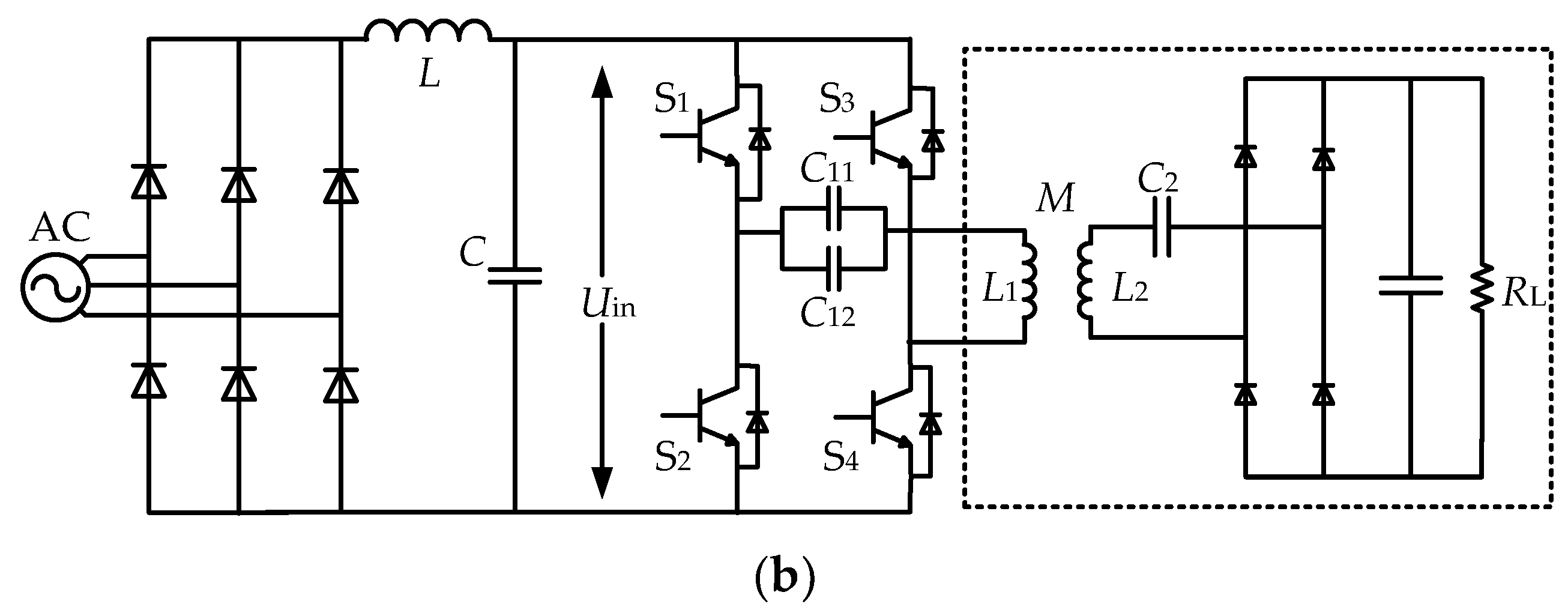
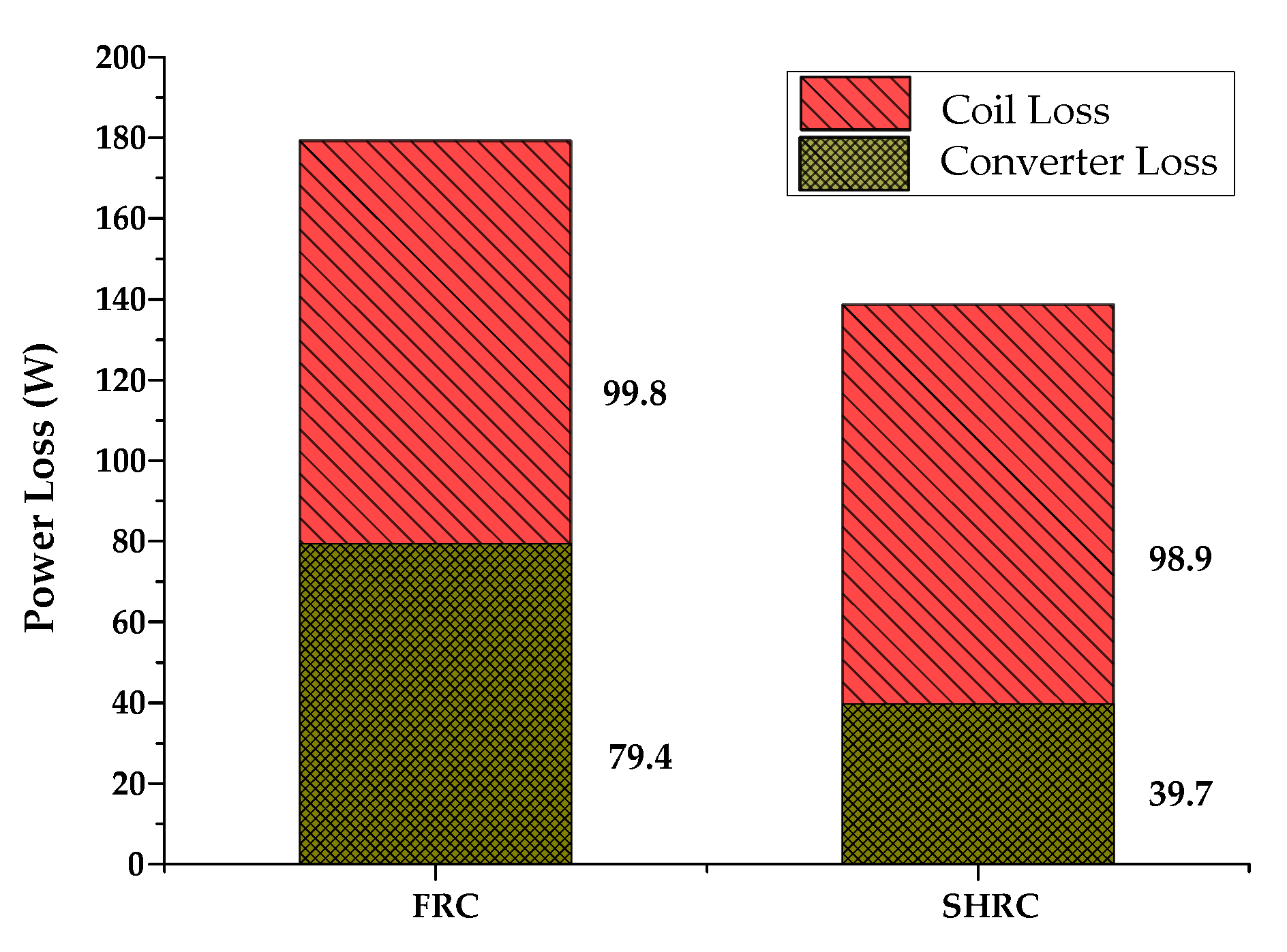
3.2. Comparison of SS/S SHRC and FRC

In this section, the efficiency comparison of SHRC and FRC is presented. For fairness, the load and output power in both topologies are set as the same using the same devices. As shown in Figure 1a,b, the same capacitors, switches, coils, and diodes are used for the SHRC and the FRC. As described in Section 2.1 and shown in Figure 5, the equivalent circuits of the two topologies are the same. The output power P2 can be calculated as
P 2 = j 2 ω 2 M 2 i 1 2 R a c ( Z 2 + R a c ) 2
Equation (35) shows that the output power is related to the primary current i1, M, and Rac. If the transfer distance and the coil structure, which affect the value of M, are the same, output power of SHRC and FRC are only related to primary current i1 powering the same load Rac. If the input voltage of SHRC is twice of the input voltage of FRC, the primary currents of both are the same based on Equation (24) and analysis in [6,7,8,23]. By regarding the circuit parts inside the dotted rectangle in both Figure 1a,b as two-port network and if the input currents of both topologies are the same, the efficiency of these two networks are equal to each other. Besides the losses of the two-port networks, the remained losses are the converter losses including switch conduction loss, diode conduction loss and capacitor conduction loss. Similar as the analysis in Section 2.1, for every operational process of FRC two switches are on. The loss of FRC Pfbloss can be expressed as
P f b l o s s = 2 i 1 U q
According to Equations (31) and (36),
P f b l o s s = 2 P h b l o s s
The loss of the full-bridge converter Pfbloss is twice that of the half-bridge converter Phbloss.
However, to supply a same power to a same load with same voltage and current stresses of the resonant tank, the SHRC system requires a higher input voltage than the FRC system. This results in a double switch voltage stress than that of the FRC system. Nevertheless, this article focuses on the loss and efficiency comparison of the two systems, regardless of that the switches in FRC can stand a twice higher voltage stress than they actually faced, which is not economical. To seek the balance between simpler circuit structure, higher efficiency, lower input voltages, and economical efficiency need to be further explored.
In summary, if the input voltage of SHRC is twice of FRC, which results in twice voltage stresses for switches in SHRC, the primary current i1 of SHRC and FRC are the same. The same i1 guarantees the same output power, the same coils, and the same secondary efficiency of both IPT systems. In addition, the loss of SHRC is half of the FRC losses at the same i1. It is shown that the SHRC IPT system is more efficient than FRC IPT system under these conditions.

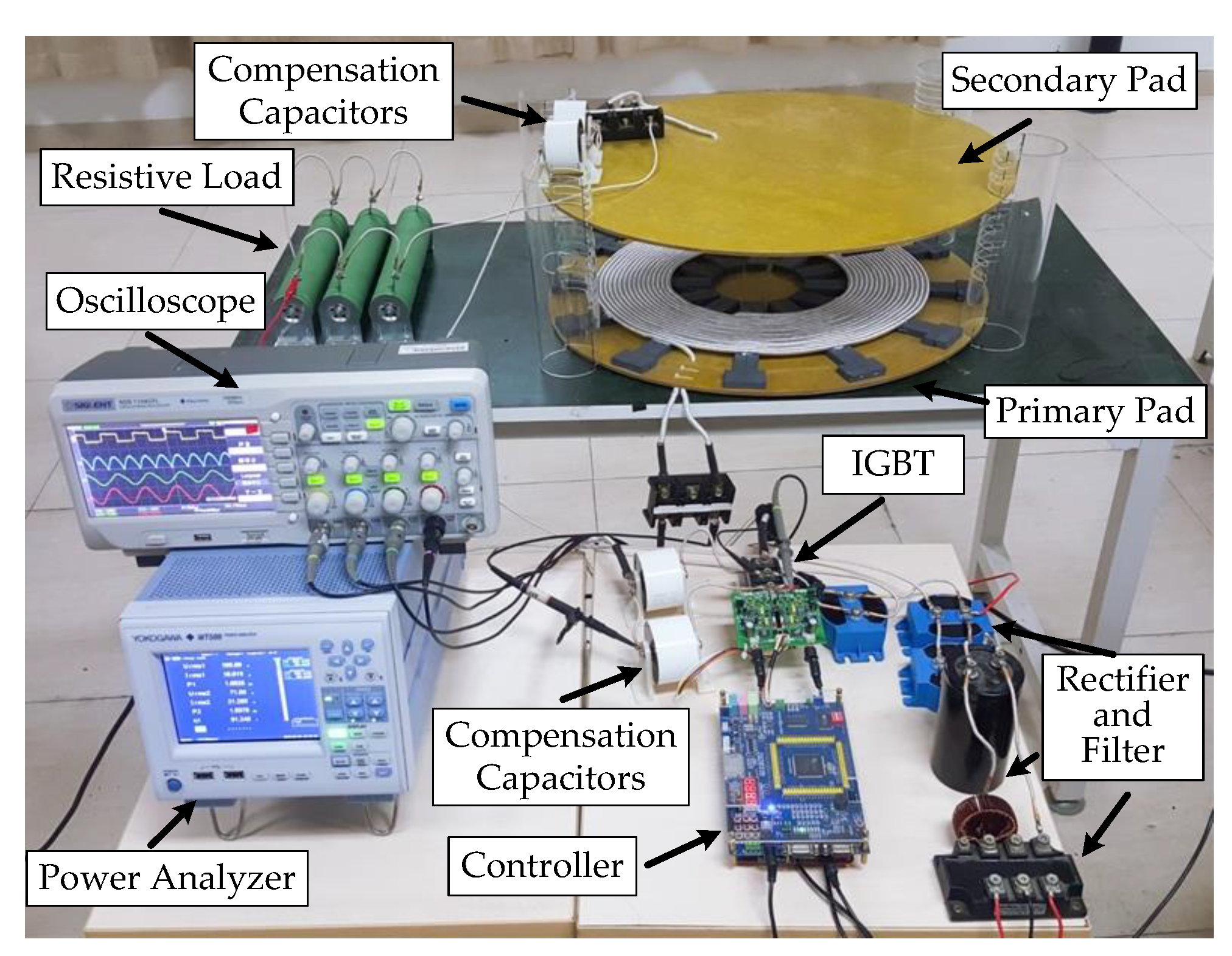
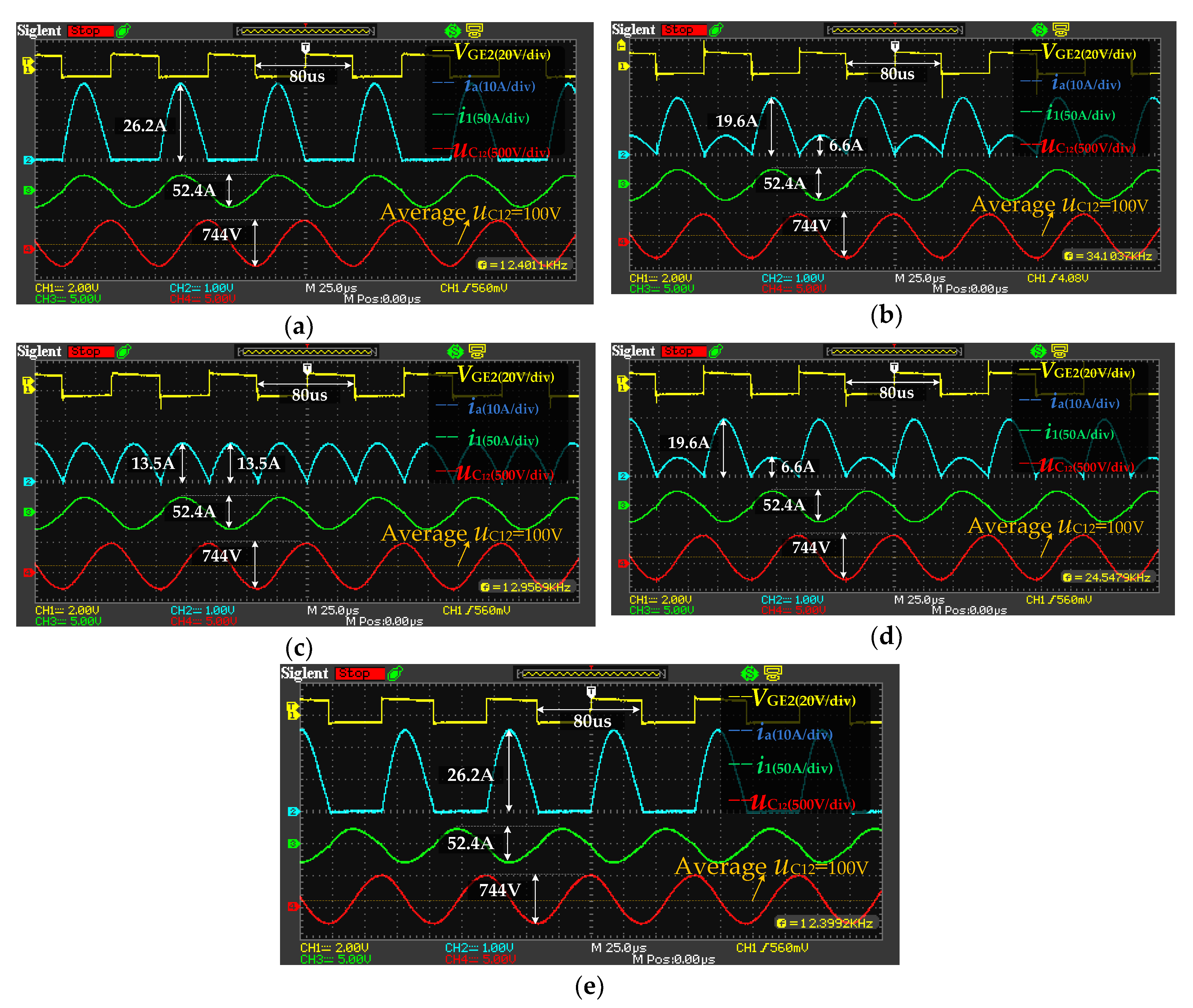
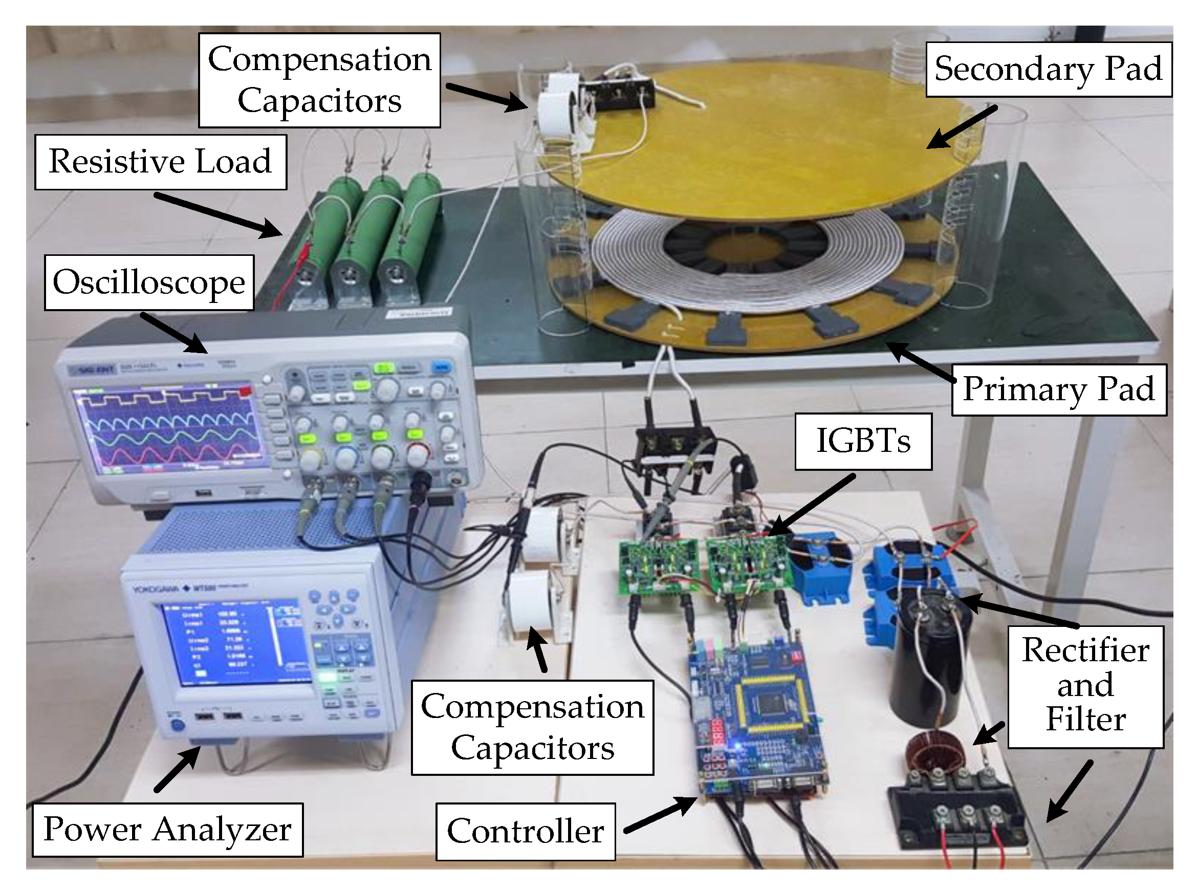
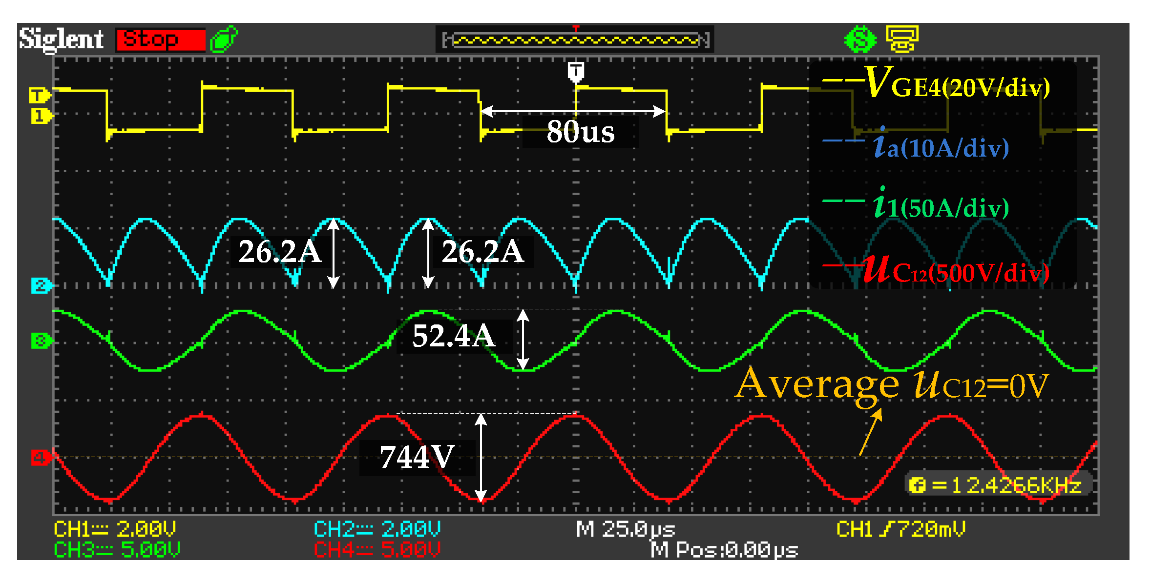
4. Simulations and Experiments

To verify the theoretical analysis proposed in this paper, a Saber simulation was established according to Figure 1a. A 1.5 kW prototype of SHRC with 170 mm air gap was built as shown in Figure 8. The parameters in the simulation and the prototype are shown in Table 1. IGBT switch model 2MBI75N-060 was used as the switches, which have a collector-emitter saturation voltage of 2.8 V at 75 A. The primary and secondary inductors were wound with Litz wires in a same manner as shown in Figure 9. Three 100 Ω resistors which were parallel with each other were used as the resistive load of the IPT system. Power analyzer WT500 was used to measure input voltages/currents, output voltages/currents, losses of SHRC, and FRC.

4.1. Operation of the Proposed SS/S SHRC

Based on the parameters of Table 1, the coupling coefficient k is 0.29, the normalized load resistance Rn is 0.25, and the resonant frequency f0 is 12.8 kHz. Frequency bifurcation would occur according to the analysis in Section 2 and Figure 7. In order to verify the frequency bifurcation, the operational frequency 12.5 kHz, which is close to and less than the resonant frequency 12.8 kHz was chosen in the simulations and experiments. At the input voltage of 200 V, the performance of SHRC was shown by simulation in Figure 10 and validated by experiments as shown in Figure 11. In Figure 10a, as shown in the circled moment, the primary current i1 is still positive at the switching moment. The phase of the current lags behind the phase of the driving voltage VGE, which means the converter operated at the inductive region with lower frequency as the frequency bifurcation indicates. Simulation waveforms of ia for five different α were presented in Figure 10b in five different colored curves. The first peak of ia is α times of the second peak coinciding with Equation (29). When C11 is equal to C12 (α = 1), the peak value of the bus current ia achieves a minimum at 13.6 A.
The operational waveforms of different α by experiments were presented as Figure 11. The driving voltage of S2 is shown in the yellow line, the bus current ia is in blue, primary current i1 is in green, and voltage waveform of C12, uC12, is in red. As shown in Figure 11, each switch operates at nearly 50% duty cycle, including a 2 μs dead-time. The system works in resonance state. The peak of the primary resonant current i1 is 26.2 A. The peak-to-peak voltage of the C12 is 744 V, and the average is 100 V, which is half of Uin1. According to the waveforms of ia in Figure 11, the value of the first peak of ia is α times of the second peak, verifying both the theoretical analysis and the simulation results. From Figure 10a and Figure 11b, by comparing the operational waveforms, and the experimental results were consistent with the simulations. Since the influences of parasitic parameters are ignored in the simulation, waveforms of simulation are larger than the experiment. Meanwhile, the deviation is within the allowable range. In general, the simulation results and the experimental waveforms of ia, i1, uC12 verify the analysis in Section 2, as shown in Equations (20)–(29).

4.2. Soft-Switching

Since the working procedures of the two switches of SS/S SHRC are complementary with dead-time, only the soft switching state of S1 was analyzed. As shown in Figure 12, the yellow curve is the driving voltage of S1, the green curve is the primary current i1, and the red curve is VCE of S1. At t0, D1 is in conducting state, VCE is 0, S1 is turned on, and i1 is zero. Thus, S1 is turned on in ZVS and ZCS state. At t1, S1 is turned off. The i1 is approximately zero. Because of the effect of parasitic capacitor, which is parallel to S1, VCE rises from zero to Uin. So, S1 turns off in ZVS and quasi-ZCS state.

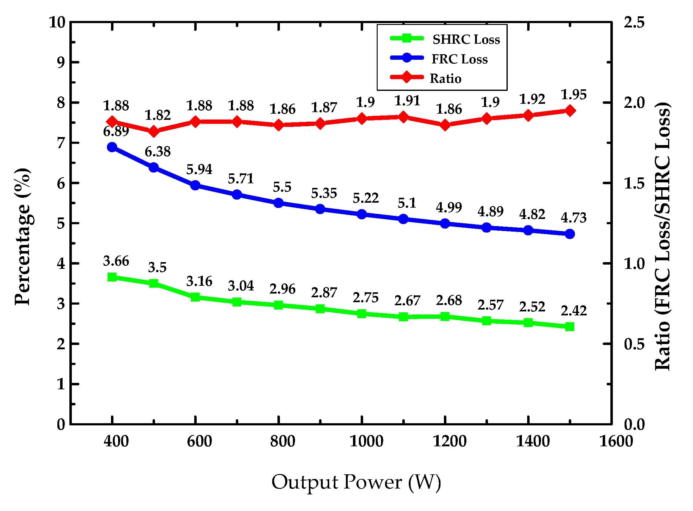
4.3. Comparison between SHRC and FRC

For a fair comparison, FRC IPT system was built with the same device as SHRC IPT system. C11, in parallel with C12, are the primary compensate capacitors which are shown in Figure 13. The experimental waveforms of FRC IPT system were presented in Figure 14. The bus current ia, peak to peak capacitor voltage uC12, primary current i1, and the resonant frequency are exactly the same as SHRC shown in Figure 10 and Figure 11. To analyze the difference between the SHRC and FRC IPT system, comparing Figure 11 with Figure 14, only the bus current ia and the average of uC12 are different. The results validate Section 2 analysis that the proposed SS/S SHRC has the same operational characteristics as the FRC.
For the converter efficiency comparison, in order to ensure the universality, a SHRC system with α = 3 was compared with the FRC. Based on the parameters in Table 1, the losses of SHRC and FRC at different output power from 400 W to 1500 W were measured by experiments and illustrated in Figure 15. The input voltage of SHRC changed from 0 V to 200 V and that of FRC from 0 V to 100 V. When the output power was 1500 W, the input voltage of SHRC was 200 V and that of FRC was 100 V verifying the analysis in Section 3.2. For a system efficiency comparison, the total efficiency is 91.6% of the SHRC IPT system, while it was 89.3% of FRC IPT system at 1500 W. Both were measured from the two experimental prototypes. At the output power of 1500 W, the coil loss and converter loss of the two systems were presented in Figure 16 for comparison.
In Figure 15, the left coordinate is the loss percentage of SHRC and FRC, whereas the right coordinate is the ratio of FRC loss to SHRC loss. It is shown that the SHRC loss (curve in green) and FRC loss (curve in blue) decrease with the increasing of transferring power in low power range, then the decreasing speed gradually slows down. According to Equation (37), the ratio of FRC loss to SHRC loss is 2. In Figure 15, it is slightly smaller than 2. The reason may because the loss of the contact resistance and other parameters of the device, which can be considered as a fixed proportion is ignored in the efficiency in Section 3. From Figure 16, the coil losses of both converters are almost the same, validating the two-port network efficiency analysis in Section 3. From the experimental results, it is verified that the SHRC IPT system is more efficient than the FRC IPT system by comparing the losses.

5. Conclusions and Discussion

In this paper, an SS/S compensated symmetrical half-bridge resonant converter for the inductive power transfer is presented. The main contributions of this paper are as followed:
1. Based on the mutual inductance model and the first harmonic approximation method, the working procedure and system parameters of the proposed converter are analyzed in detail and compared with an FRC system. In the proposed system, the pair of resonant capacitors with different capacitance ratios were applied and theoretically compared.
2. The frequency bifurcation of proposed IPT system is theoretically analyzed by impedance analysis method. In order to verify the frequency bifurcation phenomenon, an operating frequency of 12.5 kHz close to and lower than the resonant frequency of 12.8 kHz was applied to the system.
3. Simulations and experiments are done to verify the theoretical analysis. The losses and efficiencies of the proposed system with the FRC system. To supply a same power to a same load with same voltage and current stresses of the resonant tank, the SHRC system achieves a higher efficiency than the FRC system, although the SHRC system requires a higher input voltage than the FRC system. Experimental results show that the loss of SHRC was 39.7 W while that of FRC was 79.4 W, and the total efficiency is 91.6% of the SHRC IPT system compared with 89.3% of the FRC IPT system at 1500 W.
On the other hand, the proposed system will suffer twice the voltage stress of the switches in the primary compared to those of the FRC system. To seek a balance between simpler circuit structure, higher efficiency, lower input voltages, and economical efficiency need to be further explored. Comparison of the proposed topology with other converter topologies will also be explored in the future work.

Author Contributions

Conceptualization, J.H. and W.C.; methodology, J.H. and W.C.; software, J.H., Q.F. and W.W.; validation, J.H., Z.L., Q.F. and W.W.; formal analysis, W.C., J.H. and M.G.; investigation, J.H., W.W. and Z.L.; resources, W.C. and M.G.; data curation, J.H., Z.L. and M.G.; writing—original draft preparation, J.H. and M.G.; writing—review and editing, M.G.; visualization, M.G.; supervision, W.C.; project administration, W.C.; funding acquisition, W.C., W.W. and M.G.

Funding

This research was funded by National Natural Science Foundation of China (NSFC), grant number 51777177; NSFC grant number 51707168; Key Projects of Fujian Collaborative Innovation Center for R&D of Coach and Special Vehicle, grant number 2016AYF002; and Guizhou Science and Technology Department, grant number LKS[2011]19.

Conflicts of Interest

The authors declare no conflict of interest.

References

  1. Hui, S.Y. Planar Wireless Charging Technology for portable electronic products and Qi. Proc. IEEE 2013, 6, 1290–1301. [Google Scholar] [CrossRef]
  2. Arai, S.; Miura, H.; Sato, F.; Matsuki, H.; Sato, T. Examination of circuit parameters for stable high efficiency TETS for artificial hearts. IEEE Trans. Magn. 2005, 10, 4170–4172. [Google Scholar] [CrossRef]
  3. Sallan, J.; Villa, J.L.; Llombart, A.; Sanz, J.F. Optimum design of ICPT systems applied to electric vehicle battery charge. IEEE Trans. Ind. Electron. 2009, 6, 2140–2149. [Google Scholar] [CrossRef]
  4. Bi, Z.; Kan, T.; Mi, C.C.; Zhang, Y.; Zhao, Z.; Keoleian, G.A. A review of wireless power transfer for electric vehicles: Prospects to enhance sustainable mobility. Appl. Energy 2016, 179, 413–425. [Google Scholar] [CrossRef] [Green Version]
  5. Wu, H.H.; Gilchrist, A.; Sealy, K.D.; Bronson, D. A high efficiency 5 kw inductive charger for EVs using dual side control. IEEE Trans. Ind. Inform. 2012, 8, 585–595. [Google Scholar] [CrossRef]
  6. Zheng, C.; Lai, J.S.; Chen, R.; Faraci, W.E.; Ullah Zahid, Z.; Gu, B. High-efficiency contactless power transfer system for electric vehicle battery charging application. IEEE J. Emerg. Sel. Top. Power Electron. 2015, 3, 65–74. [Google Scholar] [CrossRef]
  7. Ramezani, A.; Farhangi, S.; Iman-Eini, H.; Farhangi, B.; Rahimi, R.; Moradi, G.R. Optimized LCC-Series Compensated Resonant Network for Stationary Wireless EV Chargers. IEEE Trans. Ind. Electron. 2019, 66, 2756–2765. [Google Scholar] [CrossRef]
  8. Kalwar, K.A.; Mekhilef, S.; Seyedmahmoudian, M.; Horan, B. Coil Design for High Misalignment Tolerant Inductive Power Transfer System for EV Charging. Energies 2016, 9, 937. [Google Scholar] [CrossRef]
  9. Elnail, K.E.I.; Huang, X.; Xiao, C.; Tan, L.; Haozhe, X. Core Structure and Electromagnetic Field Evaluation in WPT Systems for Charging Electric Vehicles. Energies 2018, 11, 1734. [Google Scholar] [CrossRef]
  10. Stielau, O.H.; Covic, G.A. Design of loosely coupled inductive power transfer systems. In Proceedings of the International Conference on Power System Technology, Perth, Australia, 4–7 December 2000; pp. 85–90. [Google Scholar] [CrossRef]
  11. Zhang, W.; Mi, C.C. Compensation topologies of high-power wireless power transfer systems. IEEE Trans. Veh. Technol. 2016, 65, 4768–4778. [Google Scholar] [CrossRef]
  12. Hou, J.; Chen, Q.; Wong, S.C.; Tse, C.K.; Ruan, X. Analysis and control of series/series-parallel compensated resonant converter for contactless power transfer. IEEE J. Emerg. Sel. Top. Power Electron. 2017, 3, 124–136. [Google Scholar] [CrossRef]
  13. Zhang, Y.; Chen, K.; He, F.; Zhao, Z.; Lu, T.; Yuan, L. Closed-form oriented modeling and analysis of wireless power transfer system with constant-voltage source and load. IEEE Trans. Power Electron. 2015, 31, 3472–3481. [Google Scholar] [CrossRef]
  14. Sibué, J.R.; Kwimang, G.; Ferrieux, J.P. A global study of a contactless energy transfer system: Analytical design, virtual prototyping, and experimental validation. IEEE Trans. Power Electron. 2013, 28, 4490–4698. [Google Scholar] [CrossRef]
  15. Patil, D.; McDonough, M.K.; Miller, J.M.; Fahimi, B.; Balsara, P.T. Wireless Power Transfer for Vehicular Applications: Overview and Challenges. IEEE Trans. Transp. Electrif. 2018, 4, 3–37. [Google Scholar] [CrossRef]
  16. Ge, S.; Liu, C.; Li, H.; Guo, Y.; Cai, G. Double-LCL resonant compensation network for electric vehicles wireless power transfer: Experimental study and analysis. IET Power Electron. 2016, 9, 2262–2270. [Google Scholar] [CrossRef]
  17. Li, Z.; Song, K.; Wei, G.; Jiang, J.; Zhu, C. A 3 kw wireless power transfer system for sightseeing car supercapacitor charge. IEEE Trans. Power Electron. 2017, 32, 3301–3316. [Google Scholar] [CrossRef]
  18. Zhang, W.; Wong, S.C.; Tse, C.K.; Chen, Q. Design for Efficiency Optimization and Voltage Controllability of Series-Series Compensated Inductive Power Transfer Systems. IEEE Trans. Power Electron. 2014, 29, 191–200. [Google Scholar] [CrossRef]
  19. Wang, C.S.; Stielau, O.H.; Covic, G.A. Design considerations for a contactless electric vehicle battery charger. IEEE Trans. Ind. Electron. 2005, 52, 1308–1314. [Google Scholar] [CrossRef]
  20. Villa, J.L.; Sallan, J.; Sanz Osorio, J.F.; Llombart, A. High-Misalignment Tolerant Compensation Topology For ICPT Systems. IEEE Trans. Ind. Electron. 2012, 59, 945–951. [Google Scholar] [CrossRef]
  21. Keeling, N.A.; Covic, G.A.; Boys, J.T. A unity power factor ipt pick-up for high power applications. IEEE Trans. Ind. Electron. 2010, 57, 744–751. [Google Scholar] [CrossRef]
  22. Li, W.; Zhao, H.; Li, S.; Deng, J.; Kan, T.; Mi, C.C. Integrated LCC Compensation Topology for Wireless Charger in Electric and Plug-in Electric Vehicles. IEEE Trans. Ind. Electron. 2015, 62, 4215–4225. [Google Scholar] [CrossRef]
  23. Liu, X.; Clare, L.; Yuan, X.; Wang, C.; Liu, J. A Design Method for Making an LCC Compensation Two-Coil Wireless Power Transfer System More Energy Efficient Than an SS Counterpart. Energies 2017, 10, 1346. [Google Scholar] [CrossRef]
  24. Zhang, X.; Lai, Z.; Xiong, R.; Li, Z.; Zhang, Z.; Song, L. Switching Device Dead Time Optimization of Resonant Double-Sided LCC Wireless Charging System for Electric Vehicles. Energies 2017, 10, 1772. [Google Scholar] [CrossRef]
  25. Li, S.; Mi, C.C. Wireless Power Transfer for Electric Vehicle Applications. IEEE J. Emerg. Sel. Top. Power Electron. 2015, 3, 4–17. [Google Scholar] [CrossRef]
Figure 1. Comparison of the two topologies: (a) Proposed series-series/series (SS/S) symmetrical half-bridge resonant converter (SHRC)-based inductive power transfer (IPT) system; (b) The S/S full-bridge resonant converter (FRC) based system.
Energies 12 02268 g001aEnergies 12 02268 g001b
Figure 2. Operating modes of the proposed SHRC: (a) Mode 1 [t0t1]; (b) Mode 2 [t1t2]; (c) Mode 3 [t2t3]; (d) Mode 4 [t3t4].
Energies 12 02268 g002
Figure 3. Operational waveforms of SHRC.
Energies 12 02268 g003
Figure 4. Equivalent circuit of SHRC IPT system.
Energies 12 02268 g004
Figure 5. Equivalent circuit of SHRC IPT system using harmonic approximation method.
Energies 12 02268 g005
Figure 6. Plots of impedance as a function of ωn and Rn at fixed k = 0.29: (a) The normalized primary impedance Z1n; (b) The normalized secondary impedance Z2n; (c) The normalized reflected impedance Zrn; (d) The two-dimensional figure of Z1n.
Energies 12 02268 g006
Figure 7. Impedance angle of Z1.
Energies 12 02268 g007
Figure 8. A 1.5 kW prototype of SHRC.
Energies 12 02268 g008
Figure 9. Structure of transmitter coil.
Energies 12 02268 g009
Figure 10. Simulation results: (a) Simulation waveforms of α = 3 (VGE2, bus current, primary coil current, capacitor voltage); (b) Waveforms of ia for different α.
Energies 12 02268 g010
Figure 11. Steady-state operational waveforms of different α: (a) α = ∞; (b) α = 3; (c) α = 1; (d) α = 1/3; (e) α = 0.
Energies 12 02268 g011
Figure 12. Soft-switching analysis.
Energies 12 02268 g012
Figure 13. A 1.5 kW prototype of FRC IPT system.
Energies 12 02268 g013
Figure 14. Experimental waveforms of FRC IPT system.
Energies 12 02268 g014
Figure 15. Power loss percentage of two converters.
Energies 12 02268 g015
Figure 16. Power loss distributions for the two converter-based IPT systems.
Energies 12 02268 g016
Table 1. Parameters for SHRC and FRC 1.5 kW IPT systems.
SymbolCircuit ComponentValue
Uin1SHRC input voltage0–200 V
Uin2FRC input voltage0–100 V
L1primary inductance175 μH
L2secondary inductance175 μH
C11 + C12primary capacitance880 nF
C2secondary capacitance880 nF
rL1primary coil resistance165 mΩ
rL2secondary coil resistance165 mΩ
Mmutual inductance50.5 μH
RLload resistance3.33 Ω

