Continuous-Input Continuous-Output Current Buck-Boost DC/DC Converters for Renewable Energy Applications: Modelling and Performance Assessment


Abstract
:1. Introduction
2. Average Circuit Modelling for the Considered Buck-Boost Converters
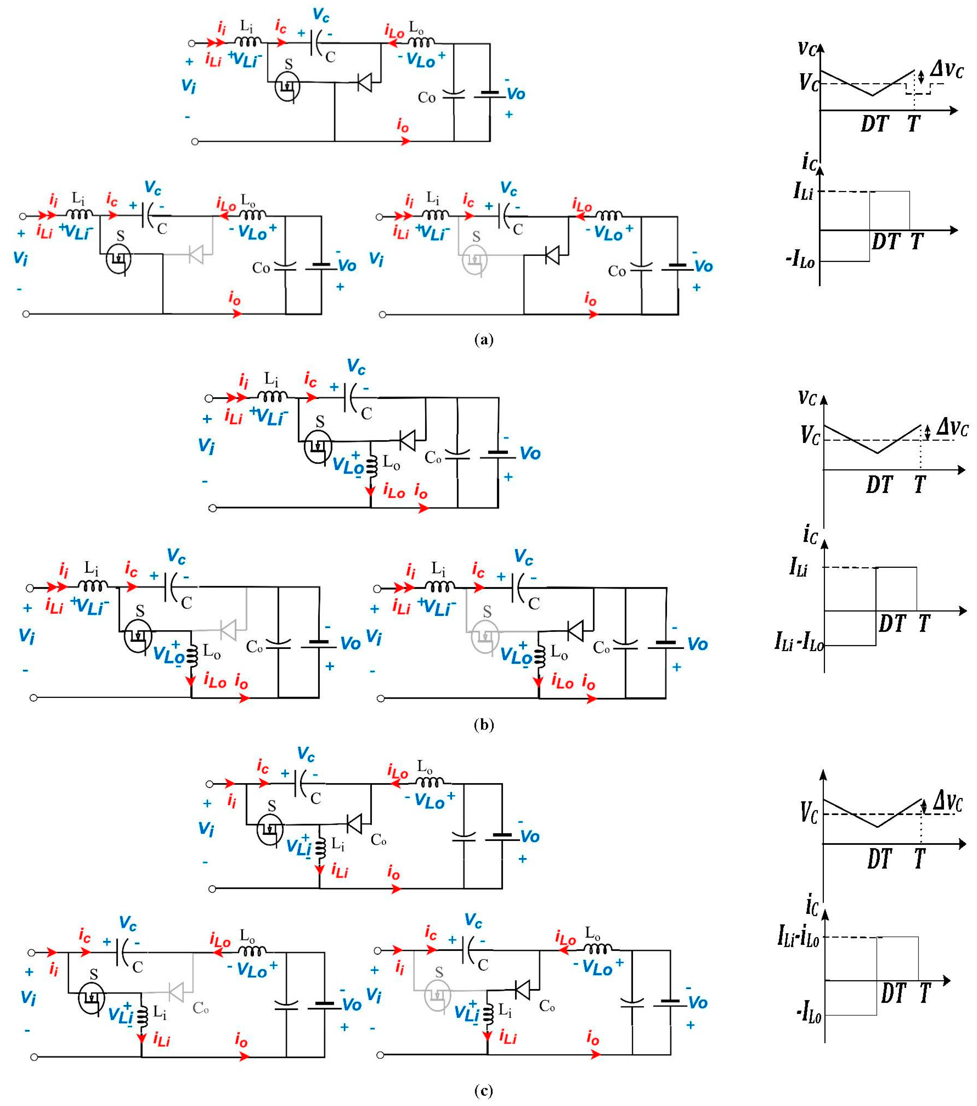
2.1. CUK Converter
2.1.1. Voltage Transfer Function Calculation
2.1.2. Inductors’ Ripple Currents Calculation
2.1.3. Input/Output Ripple Currents Calculation
2.2. D1 Converter
2.2.1. Voltage Transfer Function Calculation
2.2.2. Inductors’ Ripple Currents Calculation
2.2.3. Input/Output Ripple Currents Calculation
2.3. D2 Converter
2.3.1. Voltage Transfer Function Calculation
2.3.2. Inductors’ Ripple Currents Calculation
2.3.3. Input/output Ripple Currents Calculation
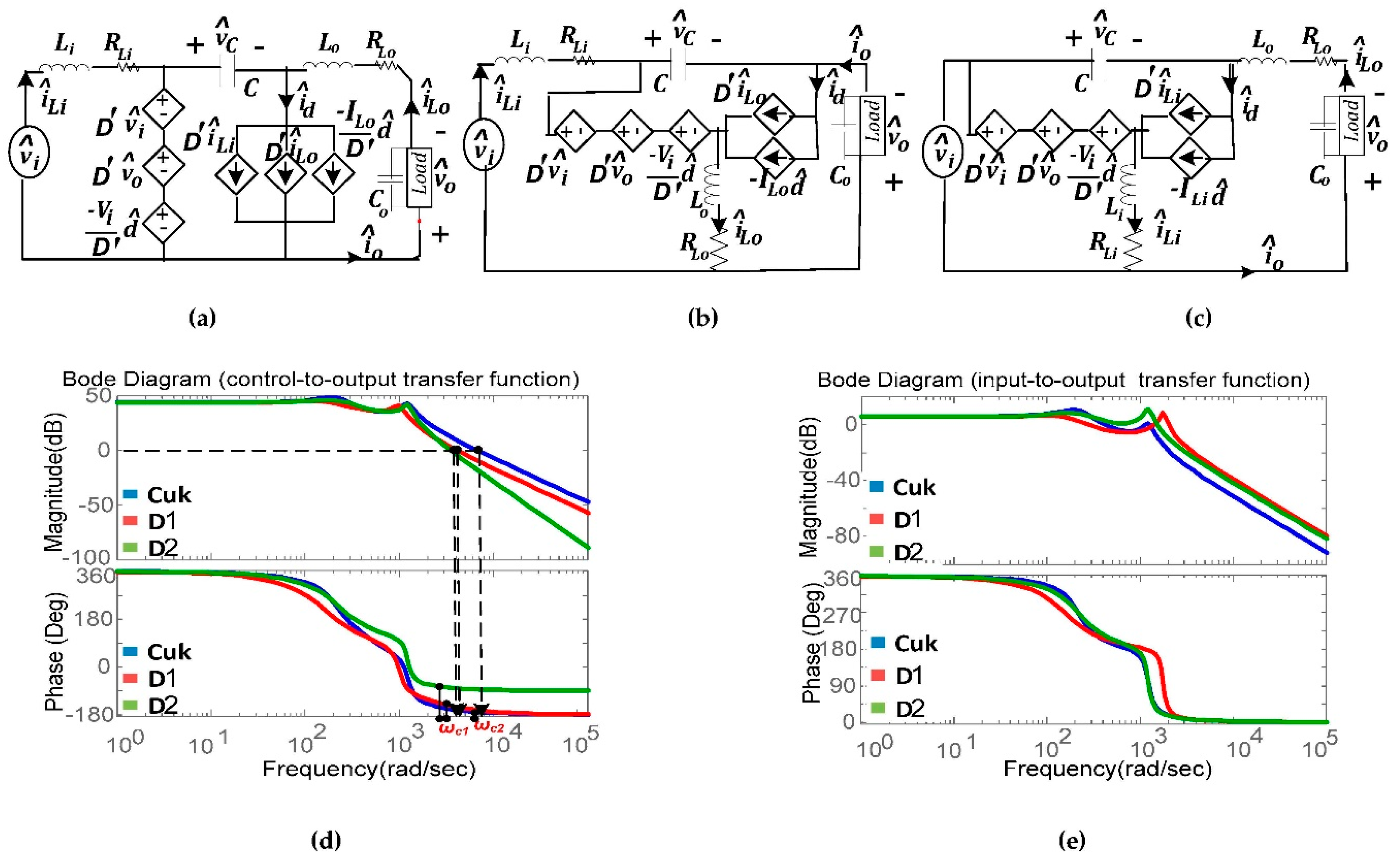
3. Small Signal Model for the Considered Buck-Boost Converters in Continuous Current Mode (CCM)
3.1. CUK Converter
3.1.1. To Get Control-to-Output Transfer Function
3.1.2. To Get Input-to-Output Transfer Function
3.2. D1 Converter
3.2.1. To Get Control-to-Output Transfer Function
3.2.2. To Get Input-to-Output Transfer Function
3.3. D2 Converter
3.3.1. To Get Control-to-output Transfer Function
3.3.2. To Get Input-to-Output Transfer Function
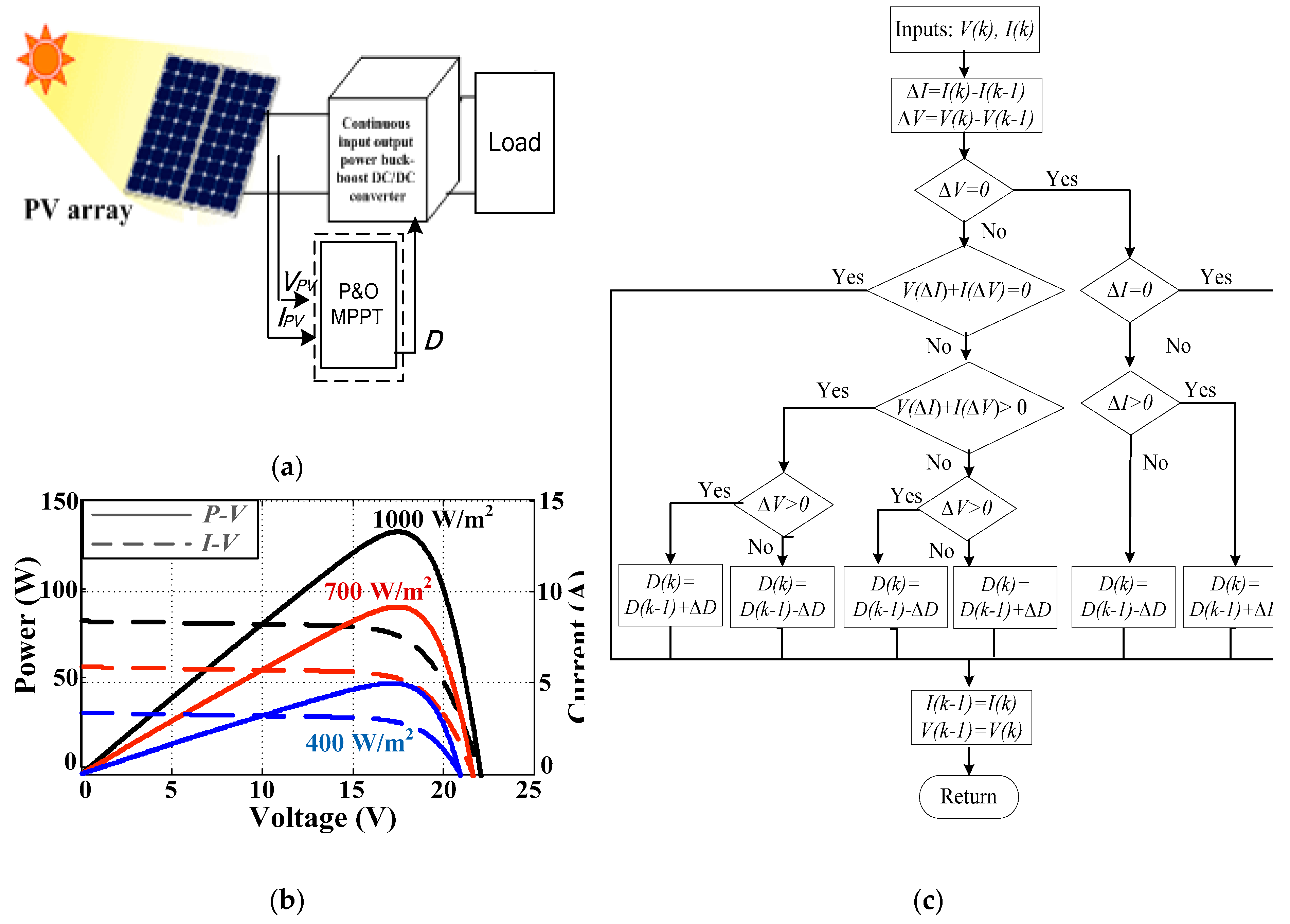
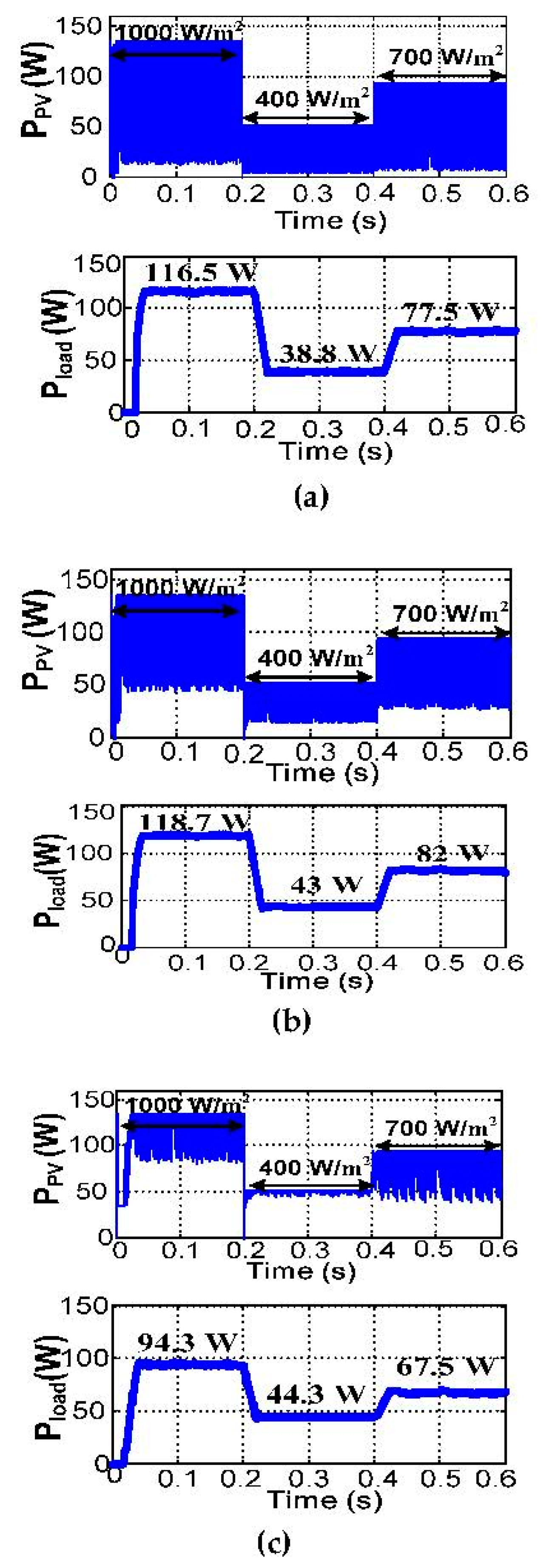
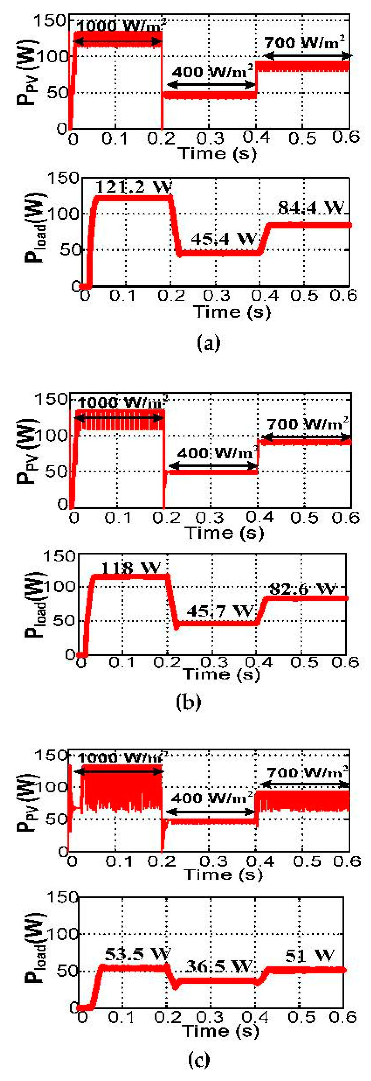
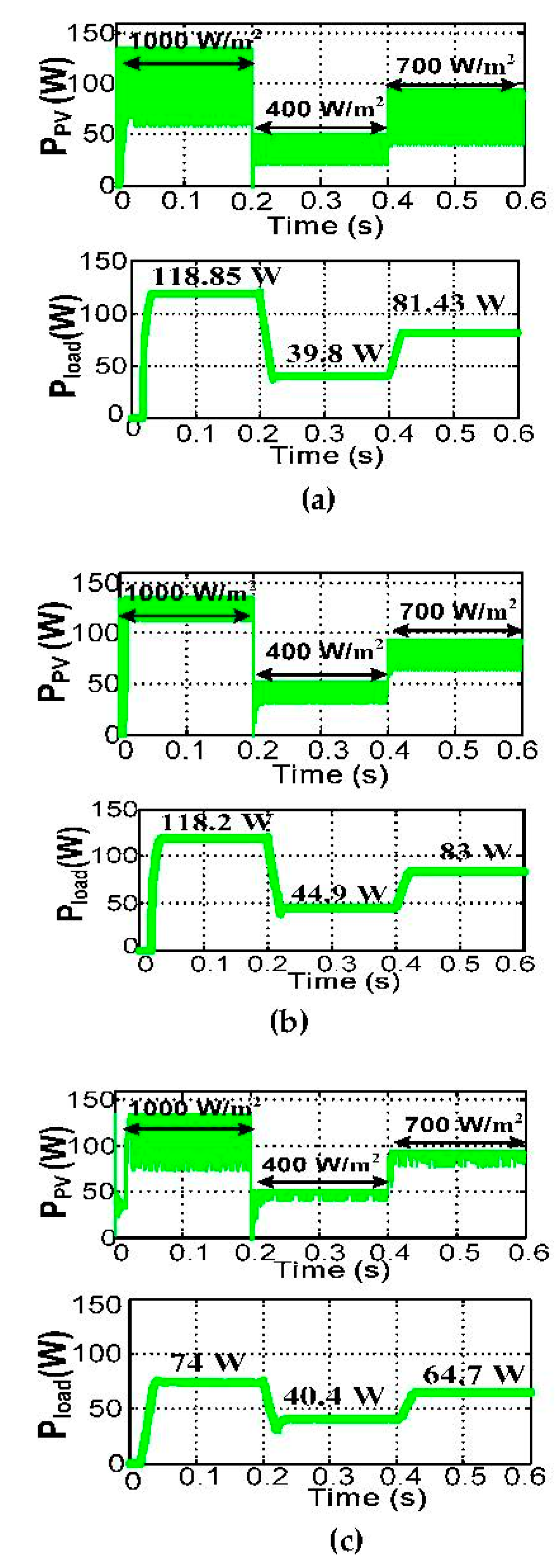
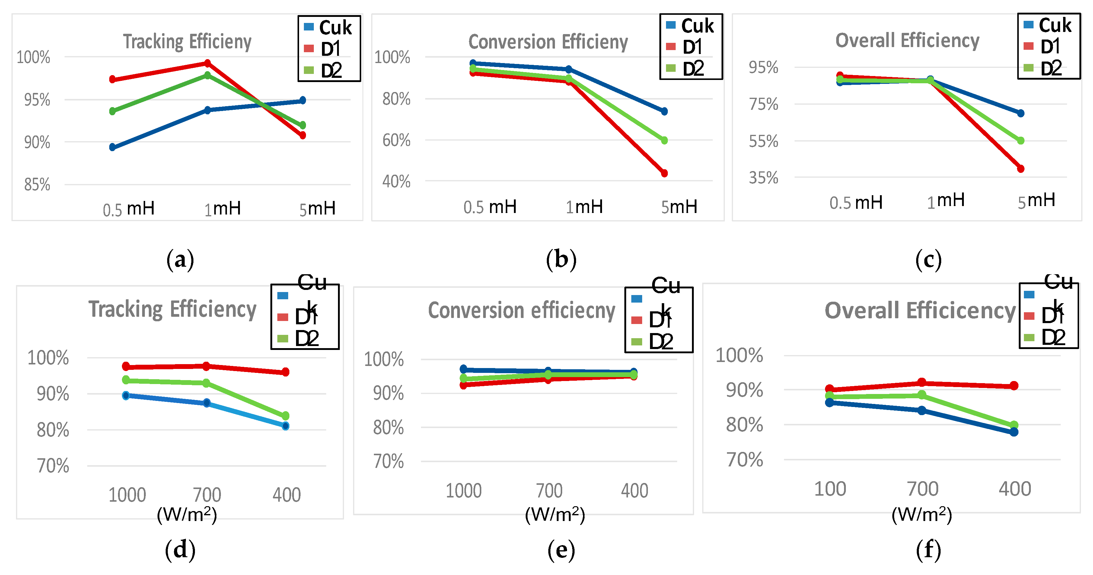
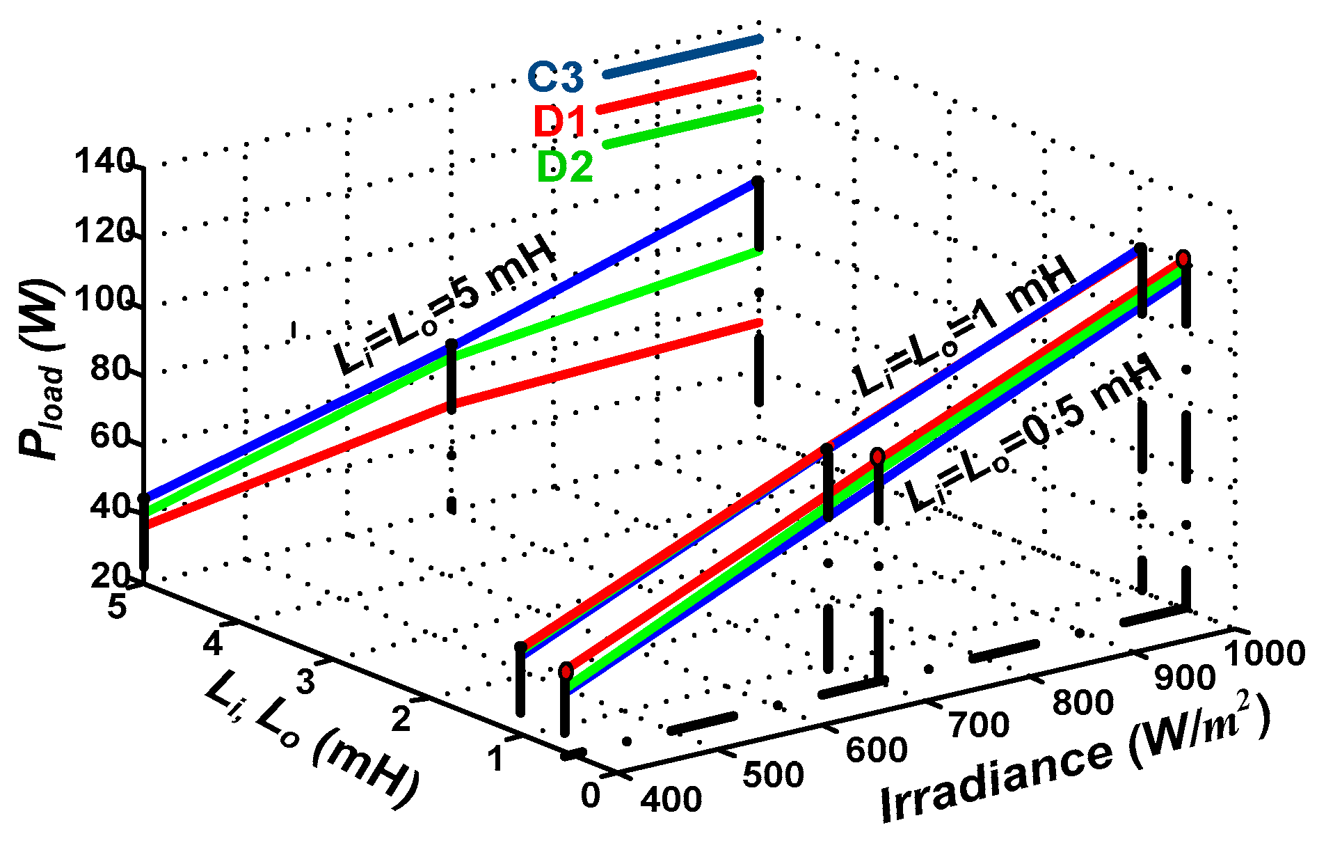
4. Simulation Results
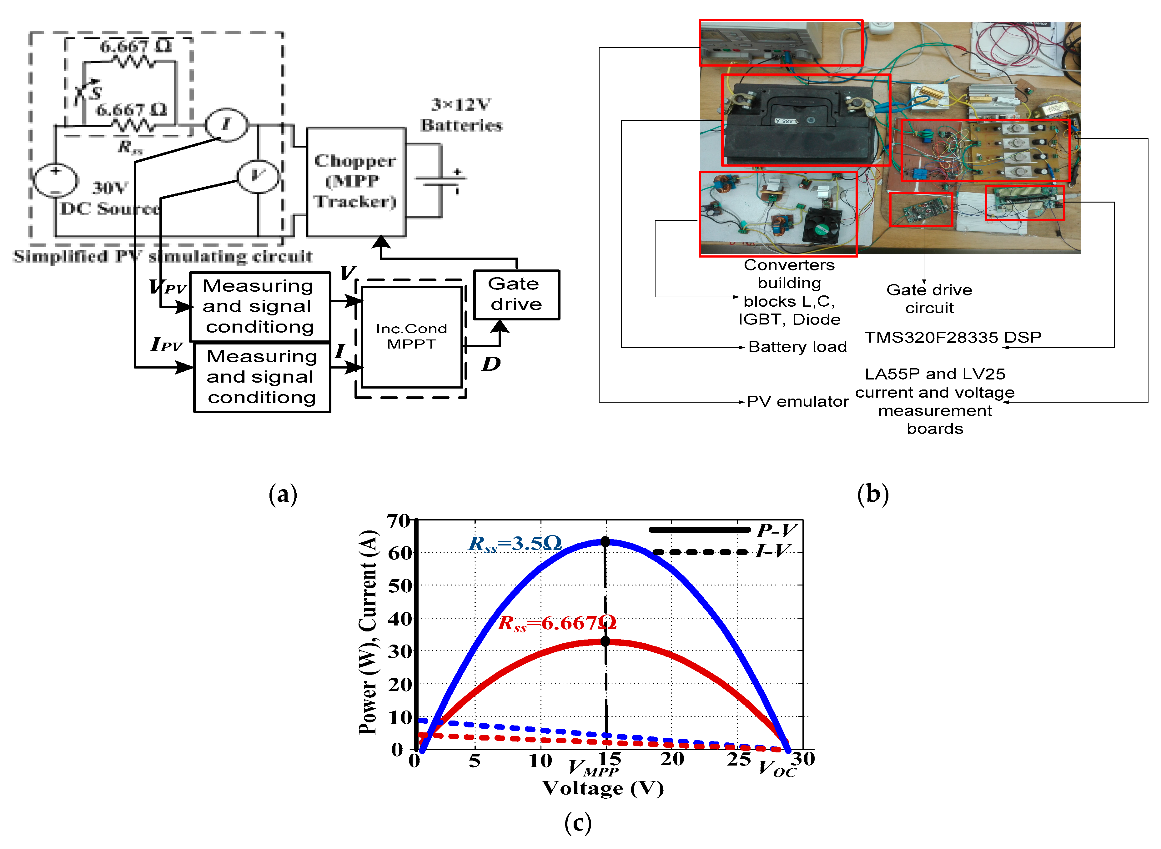
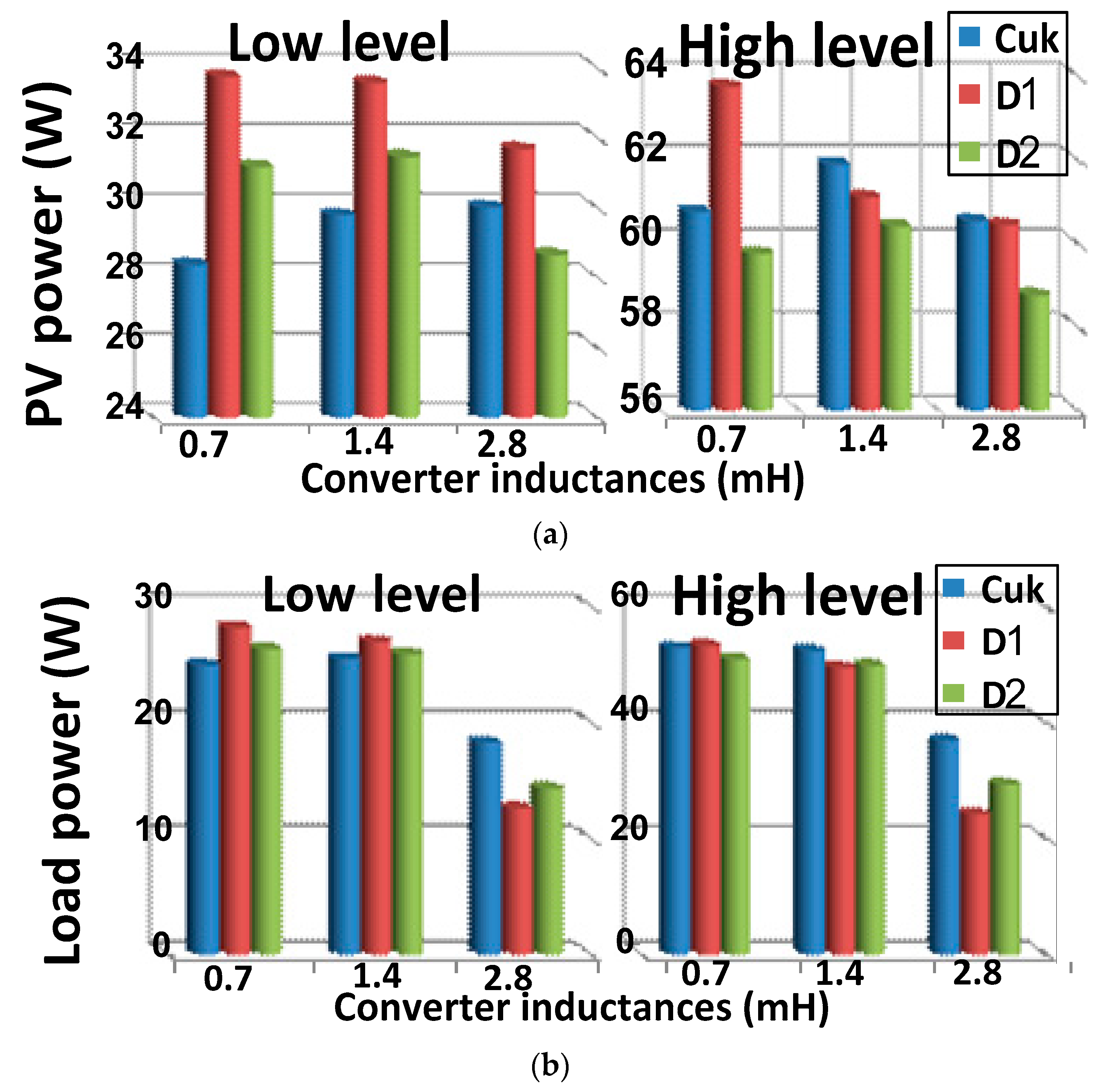
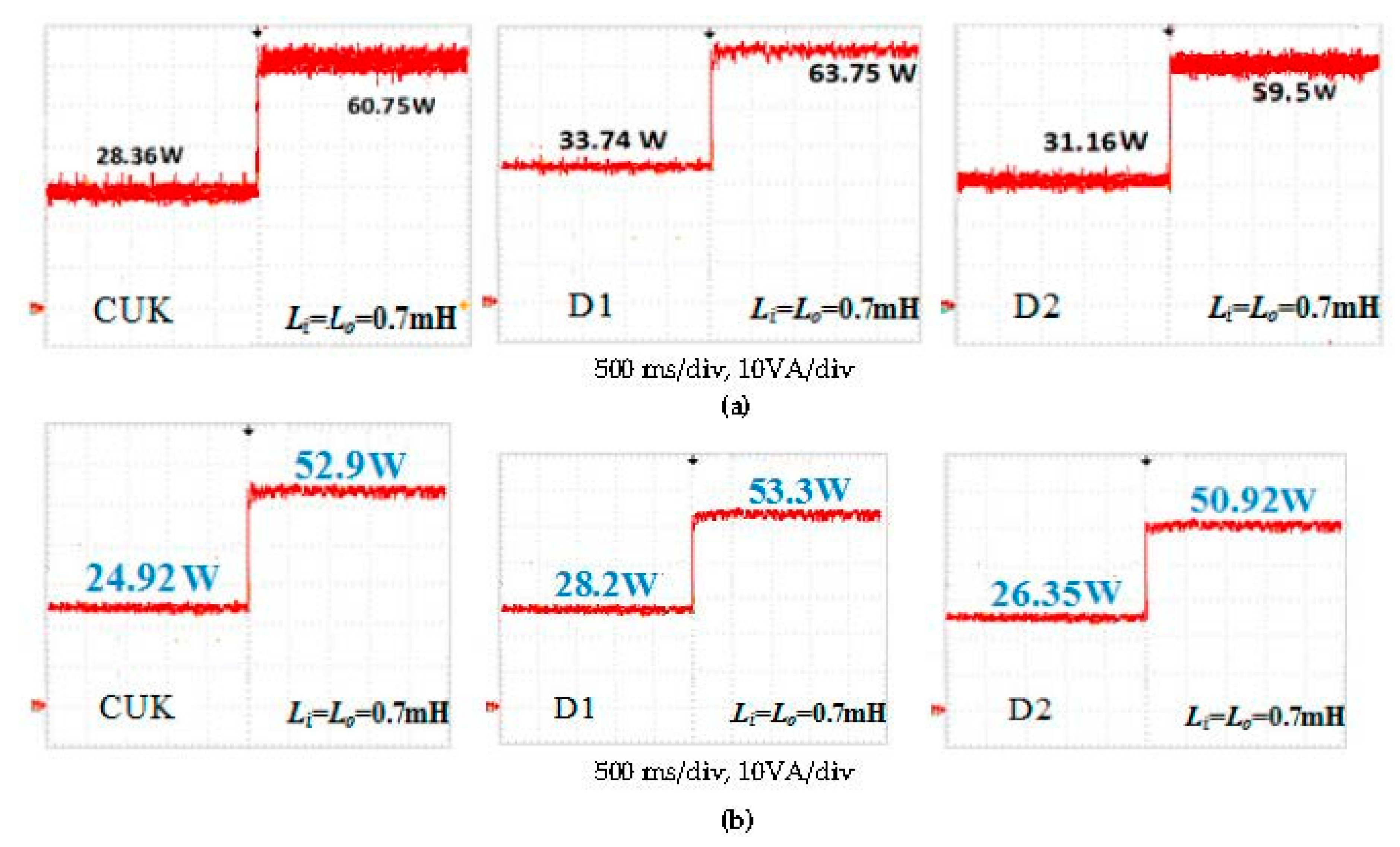
5. Experimental Results
6. Discussion
6.1. Why are the Inductance Values Used in the Simulation Different than those Used in the Experimental Verification?
- The different range of examined PV power, input and output DC voltage at the converter terminals, input and output current across the examined converter, percentage acceptable ripples in the system currents, etc… are all aspects characterizing the fact that both the simulation and experimental analysis are different and hence mandate the utilization of different converter inductances in the experimental setup in order to ensure the CCM and preserve the same acceptable power and current oscillation level. This is in order to achieve fair counterpart DC/DC converters performance assessment as the main factor in selecting the inductor values to ensure CCM is the percentage current ripples which is not the same as in simulation due to the difference in system aspects as mentioned above. The inductance values are selected just above the minimum value that ensure the CCM operation to avoid the added conduction loss that may be exerted when higher values of inductances are selected as their parasitic resistance is proportional to the inductance values.
- Comparative analysis between counterparts can be enhanced by using system parameters in the simulation that differ from that in the experimental assessment. The simulation assessment examines the investigated converters using certain inductance values and operating condition where a conclusion is deducted from this assessment. The authors perform the experimental analysis with different system parameters to emphasise that the conclusions obtained from the simulation results are still valid even if the system power, voltage/current level, oscillation percentage change. Consequently, the final conclusions are mainly converters’ trend and irrelevant to the selected inductance values. From the authors’ point of view, this way of assessment adds elaborated generalization of the obtained results emphasizing on their uniqueness irrespective from the designer selection of the converter inductances.
6.2. Why are the Investigated Converters Examined at 15 kHz, a Relatively Low Switching Frequency?
6.3. Does the Photovoltaic (PV) Generator Affect the Interfacing Converter Dynamics?
7. Conclusions
Author Contributions
Funding
Conflicts of Interest
List of Symbols
| Co | Converter output capacitor | RLi | Resistance of converter intput inductor |
| D | Switch duty ratio | RLo | Resistance of converter output inductor |
| D’ | 1- D | T | Converter switching period |
| fsw | Converter switching frequency | vi | Converter input voltage |
| ic | Capacitor current | vo | Converter output voltage |
| id | Diode current | vS | Switch voltage |
| ii | Converter input current | vc | Capacitor voltage |
| io | Converter input current | vLi | Voltage of converter input inductor |
| iLi | Current of converter input inductor | vLo | Voltage of converter output inductor |
| iLo | Current of converter output inductor | ZC | Impedance of converter link capacitor |
| Li | Converter input inductance | ZLi | Impedance of converter input inductor |
| Lo | Converter output inductance | ZLo | Impedance of converter output inductor |
| Pload | Load power | Zo | Converter output impedance |
| PPV | Tracked PV power | X | Average value of the specified quantity |
| M | Converter conversion ratio | Δx | Ripples of the specified quantity |
| Ro | Converter load resistance | Small signal term of the specified quantity |
Appendix A
| Quadratic converter [22] | 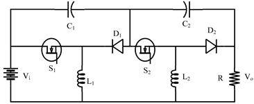 |
| Single switch Quadratic converter [21] |  |
| Boost Cascaded converter [15,16,19] | 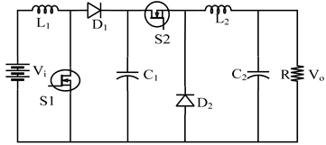 |
| Boost interleaved converter [16] |  |
| SEPIC converter [15,18] | 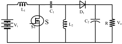 |
References
- Bose, B.K. Global Energy Scenario and Impact of Power Electronics in 21st Century. IEEE Trans. Ind. Electron. 2013, 60, 2638–2651. [Google Scholar] [CrossRef]
- Guerrero, J.M. Distributed Generation: Toward a New Energy Paradigm. IEEE Ind. Electron. Mag. 2010, 4, 52–64. [Google Scholar] [CrossRef]
- Hosenuzzamana, M.; Rahimab, N.A.; Selvaraja, J.; Hasanuzzamana, M.; Maleka, A.B.M.A.; Nahara, A. Global Prospects, Progress, Policies, and Environmental Impact of Solar Photovoltaic Power Generation. Renew. Sustain. Energy Rev. 2015, 47, 284–297. [Google Scholar] [CrossRef]
- International Energy Agency. Trends in Photovoltaic Applications: Survey Report of Selected IEA Countries between 1992 and 2013, 2014th ed.; IEA: Paris, France, 2014. [Google Scholar]
- Femia, N.; Petrone, G.; Spagnuolo, G.; Massimo, V. Power Electronics and Control Techniques for Maximum Energy Harvesting in Photovoltaic Systems, 1st ed.; CRC Press: Boca Raton, FL, USA, 2013. [Google Scholar]
- Onat, N. Recent Developments in Maximum Power Point Tracking Technologies for Photovoltaic Systems. Int. J. Photo-Energy 2010, 2010, 1–11. [Google Scholar] [CrossRef] [Green Version]
- Subudhi, B.; Pradhan, R. A Comparative Study on Maximum Power Point Tracking Techniques for Photovoltaic Power Systems. IEEE Trans. Sustain. Energy 2013, 4, 89–98. [Google Scholar] [CrossRef]
- Gomes de Brito, M.A. Evaluation of the Main MPPT Techniques for Photovoltaic Applications. IEEE Trans. Ind. Electron. 2013, 60, 1156–1167. [Google Scholar] [CrossRef]
- Zakzouk, N.E.; Elsaharty, M.A.; Abdelsalam, A.K.; Helal, A.A.; Williams, B.W. Improved Performance Low-cost Incremental Conductance PV MPPT Technique. IET Renew. Power Gener. 2016, 10, 561–574. [Google Scholar] [CrossRef]
- Islam, H.; Mekhilef, S.; Shah, N.B.M.; Soon, T.K.; Seyedmahmousian, M.; Horan, B.; Stojcevski, A. Performance Evaluation of Maximum Power Point Tracking Approaches and Photovoltaic Systems. Energies 2018, 11, 1–24. [Google Scholar] [CrossRef]
- Andrean, V.; Chang, P.C.; Lian, K.L. A Review and New Problems of Four Simple Decentralized Maximum Power Point Tracking Algorithms- Perturb and Observe, Incremental Conductance, Golden Section Search, and Newton’s Quadratic Interpolation. Energies 2018, 11, 2966. [Google Scholar] [CrossRef]
- Tymerski, R.; Vorperian, V. Generation and Classification of PWM DC-to-DC Converters. IEEE Trans. Aerosp. Electron. Syst. 1988, 24, 743–754. [Google Scholar] [CrossRef]
- Jing, C.; Bao, Y.J. Characteristics Analysis and Comparison of Buck Boost Circuit and CUK Circuit. In Proceedings of the IEEE Conference of Power Electronics Systems and Applications (PESA), Hong Kong, China, 11–13 December 2013; pp. 1–3. [Google Scholar]
- Hu, H.; Harb, S.; Kutkut, N.; Batarseh, I.; Shen, Z.J. A Review of Power Decoupling Techniques for Micro inverters with Three Different Decoupling Capacitor Locations in PV Systems. IEEE Trans. Power Electron. 2013, 28, 2711–2726. [Google Scholar] [CrossRef]
- Duran, E.; Sidrach-de-Cardona, M.; Galan, J.; Andujar, J.M. Comparative Analysis of Buck-Boost Converters used to obtain I-V Characteristic Curves of Photovoltaic Modules. In Proceedings of the IEEE Power Electronics Specialists Conference, Rhodes, Greece, 15–19 June 2008; pp. 2036–2042. [Google Scholar]
- Chen, J.; Maksimovic, D.; Erickson, R. A New Low-Stress Buck-Boost Converter for Universal-Input PPC Applications. In Proceedings of the Applied Power Electronics Conference and Exposition (APE), Anaheim, CA, USA, 4–8 March 2001; pp. 343–349. [Google Scholar]
- Kavitha, K.; Jeyakumar, E. A Synchronous Cuk Converter Based Photovoltaic Energy System Design and Simulation. Int. J. Sci. Res. Publ. 2012, 2, 1–8. [Google Scholar]
- Shiau, J.K.; Lee, M.Y.; Wei, Y.C.; Chen, B.C. Circuit Simulation for Solar Power Maximum Power Point Tracking with Different Buck-Boost Converter Topologies. Energies 2014, 7, 5027–5064. [Google Scholar] [CrossRef]
- Hebbar, S.D.; Prasad, S. Closed Loop Analysis of Cascaded Boost-Buck Converter for Renewable Energy Sources. Int. Res. J. Eng.Technol. 2016, 3, 1068–1072. [Google Scholar]
- Andrade, A.M.S.S.; Hey, H.L.; Martins, M.L.d.S. Non-pulsating Input and Output Current Cúk, SEPIC, Zeta and Forward Converters for High-voltage Step-up Applications. Electron. Lett. 2017, 53, 1276–1277. [Google Scholar] [CrossRef]
- Zhang, N.; Zhang, G.; See, K.W.; Zhang, B. A Single-Switch Quadratic Buck Boost Converter with Continuous Input Port Current and Continuous Output Port Current. IEEE Trans. Power Electron. 2017, 33, 4157–4166. [Google Scholar] [CrossRef]
- Rosas-Caro, J.C.; Valdez-Resendiz, J.E.; Mayo-Maldonado, J.C.; Alejo-Reyes, A.; Valderrabano-Gonzalez, A. Quadratic Buck-Boost Converter with Positive Output-voltage and Minimum Ripple Point Design. IET Power Electron. 2018, 11, 1306–1313. [Google Scholar] [CrossRef]
- Williams, B.W. DC-to-DC Converters with Continuous Input and Output Power. IEEE Trans. Power Electron. 2013, 28, 2307–2316. [Google Scholar] [CrossRef]
- Williams, B.W. Generation and Analysis of Canonical Cell DC-to-DC Converters. IEEE Trans. Ind. Electron. 2013, 61, 329–346. [Google Scholar] [CrossRef]
- El Khateb, A.H.; Abd Rahim, N.; Selvaraj, J.; Williams, B.W. DC-to-DC Converter with Low Input Current Ripple for Maximum Photovoltaic Power Extraction. IEEE Trans. Ind. Electron. 2015, 62, 2246–2256. [Google Scholar] [CrossRef]
- Poorali, B.; Adib, E.; Farzanehfard, H. Small-Signal Modeling of Open-Loop PWM Z-source Converter by Circuit-Averaging Technique. IET Power Electron. 2017, 10, 1679–1686. [Google Scholar] [CrossRef]
- Kathi, L.; Ayachit, A.; Saini, D.K.; Chadha, A.; Kazimierczuk, M.K. Open-Loop Small-Signal Modeling of CUK DC-DC Converter in CCM by Circuit-Averaging Technique. In Proceedings of the IEEE Texas Power and Energy Conference, College Station, TX, USA, 8–9 February 2018. [Google Scholar]
- Erickson, N.W.; Maksimovic, D. Fundamentals of Power Electronics; Springer: Berlin, Germany, 1997. [Google Scholar]
- Zakzouk, N.E.; Abdelsalam, A.K.; Helal, A.A.; Williams, B.W. PV Single-Phase Grid-Connected Converter: DC-Link Voltage Sensorless Prospective. IEEE J. Emerg. Sel. Top. Power Electron. 2017, 5, 526–546. [Google Scholar] [CrossRef]
- Lyi, S.; Dougal, R.A. Dynamic multiphysics model for solar array. IEEE Trans. Energy Convers. 2002, 17, 285–294. [Google Scholar]
- Wyatt, J.; Chua, L. Nonlinear resistive maximum power theorem with solar cell application. IEEE Trans. Circuits Syst. 1983, 30, 824–828. [Google Scholar] [CrossRef]
- Sitbon, M.; Leppäaho, J.; Suntio, T.; Kuperman, A. Dynamics of photovoltaic-generator-interfacing voltage-controlled buck power stage. IEEE J. Photovolt. 2015, 5, 633–640. [Google Scholar] [CrossRef]
- Glass, M.C. Advancements in the Design of Solar Array to Battery Charge Current Regulators. In Proceedings of the IEEE Power Electronics Specialists Conference, Palo Alto, CA, USA, 14–16 June 1977; pp. 346–350. [Google Scholar]
- Kivimäki, J.; Kolesnik, S.; Sitbon, M.; Suntio, T.; Kuperman, A. Revisited perturbation frequency design guideline for direct fixed-step maximum power tracking algorithms. IEEE Trans. Ind. Electron. 2017, 64, 4601–4609. [Google Scholar] [CrossRef]
- Suntio, T.; Viinamäki, J.; Jokipii, J.; Messo, T.; Kuperman, A. Dynamic characterization of power electronic interfaces. IEEE J. Emerg. Sel. Top. Power Electron. 2014, 2, 949–961. [Google Scholar] [CrossRef]
- Leppäaho, J.; Suntio, T. Dynamic characteristics of current-fed superbuck converter. IEEE Trans. Power Electron. 2010, 26, 200–209. [Google Scholar] [CrossRef]
- Suntio, T. Dynamic Profile of Switched-Mode Converter: Modeling, Analysis and Control; Wiley-VCH: Weinheim, Germany, 2009. [Google Scholar]


| Converter Topology | Component Count | Switches and Diodes Voltage Stress | Merits | Limitations | ||||
|---|---|---|---|---|---|---|---|---|
| Switch | Diode | L | C | |||||
| Quadratic converter [22] | Positive Vo D1 = D2 = D | 2 | 2 | 2 | 2 | S1: , S2: d1: , d2: | * High quadratic gain * Positive output voltage | High component count |
| Single switch Quadratic converter [21] | Negative Vo | 1 | 5 | 3 | 3 | S: , d1 = d4: d2 = d5:, d3: | * Quadratic gain | * High component count * Inverted voltage |
| Boost Cascaded converter [15,16,19] | Positive Vo | 2 | 2 | 2 | 2 | S1: , S2: d1: , d2: | * Less stress on switches and diodes * Positive output voltage | High component count |
| Boost interleaved converter [16] | Positive Vo | 2 | 2 | 2 | 2 | S1: , S2: d1: , d2: | * Less stress on switches and diodes * Positive output voltage | High component count |
| SEPIC converter [15,18] | Positive Vo | 1 | 1 | 2 | 2 | S: = d: = | * Low component count * Positive output voltage | Pulsating discontinuous output current |
| CUK converter [13,15,17] | Negative Vo | 1 | 1 | 2 | 2 | S: = d: = | Continuous input/output current at Least component count | Inverted output voltage |
| D1 converter | Negative Vo | 1 | 1 | 2 | 2 | S: = d: = | Continuous input/output current at Least component count | Inverted output voltage |
| D2 converter | Negative Vo | 1 | 1 | 2 | 2 | S: = d: = | Continuous input/output current at Least component count | Inverted output voltage |
| Inductor Losses Indicator (ILi2 + ILo2)/ Ii2 [23] | Input Ripple Current | |
|---|---|---|
| CUK converter | ||
| D1 converter | ||
| D2 converter |
| Li = Lo | CUK | D1 | D2 | |||||||
|---|---|---|---|---|---|---|---|---|---|---|
| 1000 W/m2 | 400 W/m2 | 700 W/m2 | 1000 W/m2 | 400 W/m2 | 700 W/m2 | 1000 W/m2 | 400 W/m2 | 700 W/m2 | ||
| 0.5 mH | ∆IPV (A) | ±1 | ±0.75 | ±0.9 | ±0.3 | ±0.2 | ±0.4 | ± 1 | ± 0.75 | ± 0.85 |
| PPV (W) | 120.5 | 40.4 | 80.5 | 131.4 | 47.85 | 89.85 | 126.3 | 41.8 | 85.5 | |
| ζMPPT | 89.3% | 80.8% | 87.3% | 97.3% | 95.7% | 97.45% | 93.56% | 83.6% | 92.7% | |
| Pload (W) | 116.5 | 38.8 | 77.5 | 121.2 | 45.4 | 84.4 | 118.85 | 39.8 | 81.43 | |
| ζconver | 96.7% | 96% | 96.3% | 92.23% | 94.87% | 93.9% | 94.1% | 95.2% | 95.2% | |
| ζtotal | 86.3% | 77.6% | 84% | 90% | 91% | 91.5% | 88% | 79.6% | 88.3% | |
| 1 mH | ∆IPV (A) | ±0.75 | ±0.5 | ± 0.7 | ±0.175 | ±0.15 | ±0.2 | ± 0.7 | ± 0.45 | ± 0.5 |
| PPV (W) | 126.5 | 45 | 86.2 | 133.9 | 49.4 | 92.3 | 132 | 47.87 | 90.4 | |
| ζMPPT | 93.7% | 90% | 93.5% | 99.2% | 98.8% | 100% | 97.8% | 95.7% | 97.9% | |
| Pload(W) | 118.7 | 43 | 82 | 118 | 45.7 | 82.6 | 118.2 | 44.9 | 83 | |
| ζconver | 93.8% | 94.9% | 95.1% | 88.1% | 92.5% | 89.5% | 89.5% | 93.8% | 91.8% | |
| ζtotal | 87.9% | 85.4% | 88.9% | 87.5% | 91.4% | 89.6% | 87.5% | 89.8% | 89.9% | |
| 5 mH | ∆IPV (A) | ±0.5 | ±0.15 | ±0.4 | ±0.6 | ±0.2 | ±0.3 | ± 0.7 | ±0.2 | ±0.35 |
| PPV (W) | 128 | 50.3 | 84.7 | 122.5 | 49.2 | 88 | 124 | 50.2 | 92.1 | |
| ζMPPT | 94.8% | 100% | 91.9% | 90.7% | 98.4% | 95.4% | 91.85% | 100% | 99.8% | |
| Pload(W) | 94.3 | 44.3 | 67.5 | 53.5 | 36.5 | 51 | 74 | 40.4 | 64.7 | |
| ζconver | 73.7% | 88.6% | 79.7% | 43.67% | 74.2% | 57..95 | 59.7% | 80.47% | 70.2% | |
| ζtotal | 69.8% | 88.6% | 73.2% | 39.6% | 73% | 55.3% | 54.8% | 80.47% | 70.1% | |
| Li = Lo | CUK (C3) | D1 | D2 | ||||
|---|---|---|---|---|---|---|---|
| Low Power | High Power | Low Power | High Power | Low Power | High Power | ||
| 0.7 mH | ζtotal | 73.8% | 82.3% | 83.5% | 82.9% | 78% | 79.2% |
| 1.4 mH | ζtotal | 75.6% | 81.5% | 80 % | 77% | 76. 7% | 77.4% |
| 2.8 mH | ζtotal | 54.2 % | 57.4% | 37. 3% | 37.6% | 42.4% | 45.7% |
© 2019 by the authors. Licensee MDPI, Basel, Switzerland. This article is an open access article distributed under the terms and conditions of the Creative Commons Attribution (CC BY) license (http://creativecommons.org/licenses/by/4.0/).
Share and Cite
Zakzouk, N.E.; Khamis, A.K.; Abdelsalam, A.K.; Williams, B.W. Continuous-Input Continuous-Output Current Buck-Boost DC/DC Converters for Renewable Energy Applications: Modelling and Performance Assessment. Energies 2019, 12, 2208. https://doi.org/10.3390/en12112208
Zakzouk NE, Khamis AK, Abdelsalam AK, Williams BW. Continuous-Input Continuous-Output Current Buck-Boost DC/DC Converters for Renewable Energy Applications: Modelling and Performance Assessment. Energies. 2019; 12(11):2208. https://doi.org/10.3390/en12112208
Chicago/Turabian StyleZakzouk, Nahla E., Ahmed K. Khamis, Ahmed K. Abdelsalam, and Barry W. Williams. 2019. "Continuous-Input Continuous-Output Current Buck-Boost DC/DC Converters for Renewable Energy Applications: Modelling and Performance Assessment" Energies 12, no. 11: 2208. https://doi.org/10.3390/en12112208
APA StyleZakzouk, N. E., Khamis, A. K., Abdelsalam, A. K., & Williams, B. W. (2019). Continuous-Input Continuous-Output Current Buck-Boost DC/DC Converters for Renewable Energy Applications: Modelling and Performance Assessment. Energies, 12(11), 2208. https://doi.org/10.3390/en12112208