Article

A General Transformer Evaluation Method for Common-Mode Noise Behavior

1
College of Electrical Engineering, Fuzhou University, Fuzhou 350001, China
2
Fujian Key Laboratory of New Energy Generation and Power Conversion, Fuzhou 350108, China
*
Author to whom correspondence should be addressed.
Energies 2019, 12(10), 1984; https://doi.org/10.3390/en12101984
Submission received: 29 April 2019 / Revised: 17 May 2019 / Accepted: 20 May 2019 / Published: 23 May 2019
(This article belongs to the Special Issue Power Transformer Condition Assessment)

Abstract

:
In isolated power converters, the transformer is a key part of voltage transformation and isolation. Since common-mode (CM) noise is rather difficult to suppress compared with different-mode (DM) noise, more and more scholars are paying attention to the characteristics of CM noise, especially in high-frequency CM noise behaviors. CM noise can be further divided into conducted CM noise and radiated CM noise, and the main focus of this paper is on conducted CM noise. The CM coupling capacitance of the transformer is one of the main contributors of CM noise, which has been verified in many previous studies. Hence, eliminating the CM noise in a transformer coupling path can significantly lower the whole CM noise level of the converter. Professional conducted electromagnetic interference (EMI) testing instruments are quite expensive. In this paper, a general transformer evaluation technique for CM noise behavior is proposed. Only a signal generator and oscilloscope can achieve transformer CM noise behavior evaluation. PCB planar flyback transformers are designed, and a series of noise spectrums and voltage waveforms can verify the effectiveness of the proposed transformer evaluation method. The flyback adapter porotype can pass the EMI standard limited line EN55022 class B by the proposed evaluation method.

Graphical Abstract

1. Introduction

Switch-mode power supplies (SMPSs) have been widely used in both high power applications and low power applications. The flyback converter is one of the most commonly used topologies, especially in low power isolated converters such as mobile phone chargers, laptop power adapters, etc. Higher switching frequency and higher power density are the future development tendencies for isolated power converters, in order to achieve lower cost and smaller volume size. The efficiency, power density, and electromagnetic compatibility (EMC) are the key factors for power supplies, but they contradict each other. Since a higher switching frequency is helpful to achieve higher power density, it also brings many challenges in electromagnetic interference (EMI) issues. Figure 1 shows the propagation paths of electromagnetic interference noise in the isolated power converter. Generally, EMI noise can be categorized into conduction emission (CE), EMI noise, and radiation emission (RE) EMI noise. For radiation emission EMI noise, it will radiate electromagnetic energy into space, which will be received by the antenna. Then, the EMI receiver will display the noise spectrum of RE EMI noise. For conductive emission EMI noise, it can be further decoupled as different-mode (DM) noise and common-mode (CM) noise according to its propagation path. For DM noise, it will flow through L and N lines in the opposite direction. For CM noise, it will flow through L and N lines in the same direction to ground. The CM noise is harder to be suppressed compared to the DM noise because of its complex conduction paths influenced by stray inductive parameters and capacitive parameters. Besides, the generation and conduction mechanism of the CM noise is not well-known or well-modeled, especially in high-frequency ranges. The interwinding capacitance of the transformer and the parasitic capacitance between the drain of primary MOSFET and the ground are the main CM noise conduction paths [1]. Eliminating the CM noise flowing through transformer coupling path can significantly lower the whole CM noise level of the converter, which is helpful to pass the EMI standard limited lines EN55022 class B [2]. Besides, magnetic components, such as CM chock, DM chock, and transformer, also exhibit leakage of magnetic flux, which will cause near-field coupling and worsen the filtering effect of the EMI filter [3].
A series of CM noise eliminating techniques have been proposed in [4,5,6,7,8,9,10], and these techniques can be mainly categorized into two types: The first is to eliminate the CM noise flowing through the parasitic capacitance between the drain of the primary MOSFET and the ground. For this part of CM noise, if the heatsink is attached to the primary MOSFET, it will, via the parasitic capacitance between the heatsink and the ground to line impedance stabilization network (LISN) [11]. If the heatsink is connected to the primary ground, this part of the CM noise will not flow to LISN, it will just circulate internally between the primary side and the heatsink. The second is to optimize the design of the transformer in order to attenuate the CM noise flowing through the coupling capacitance of the transformer. Scholars have proposed many kinds of noise cancellation techniques [5,6,12,13]. Adding Y-cap can make the CM noise flowing through the interwinding capacitance of the transformer circulate internally instead of being detected by LISN. However, if the capacitance of the Y-cap is too large this technique may cause large leakage current [4], which is harmful to the human body. Besides, isolated power converters without a Y-cap are the development tendency in the future. Adding double shielding copper foil between the adjacent primary and secondary windings can totally eliminate CM noise in the transformer path, but this technique is impractical since it will increase the manufacturing cost, winding loss, and complicate the manufacturing process [5]. The basic CM noise balance principle of [6,7] is to achieve zero voltage difference between the adjacent primary and secondary winding layers, which can make sure that the induced electric charge in the secondary side is equal to zero. Then there is no CM current flowing through transformer coupling path. Hence, [5] proposed that adjusting the winding arrangement of the primary and secondary wining layers can achieve voltage potential balance between the adjacent primary and secondary winding layers. This method will limit the flexibility of the winding arrangement.
There are many studies analyzing the modeling of the parasitic capacitance of the transformer. Reference [12] proposed that the parasitic capacitance of a transformer with two windings can be modeled with six capacitances to apply the energy conservation. However, this model is too complex to achieve circuit analysis. The equivalent lumped capacitance is used to represent the CM noise behavior of the transformer [7,13,14,15], which can keep the displacement current rule. Then, the CM noise behaviors of the isolated power converters such as flyback converter, forward converter, and LLC resonant converter are analyzed in [7,8] based on displacement current rule. With the help of the previous efforts [7,8,12,13,14,15,16], this paper will propose a general transformer evaluation method for CM noise behavior. Only a signal generator and an oscilloscope can effectively evaluate the CM noise behavior of the transformer in the low-frequency range, which is easy to be implemented without the expensive cost of the professional CE EMI testing instruments.
This paper is organized as follows. In Section 2, the capacitance model of the transformer is first introduced for CM noise analysis. Based on the model, the CM noise flowing characteristic in the transformer coupling path is analyzed under different circuit configurations. In Section 3, the displacement current flowing through transformer coupling path under different winding arrangements is calculated. In Section 4, a general transformer evaluation method for CM noise behavior is proposed, and some key factors are also analyzed and discussed in detail. In Section 5, several transformers with different winding configurations are used to evaluate by the proposed method, and the measured noise spectrums can verify the effectiveness of the proposed evaluation method. Section 6 concludes this paper.

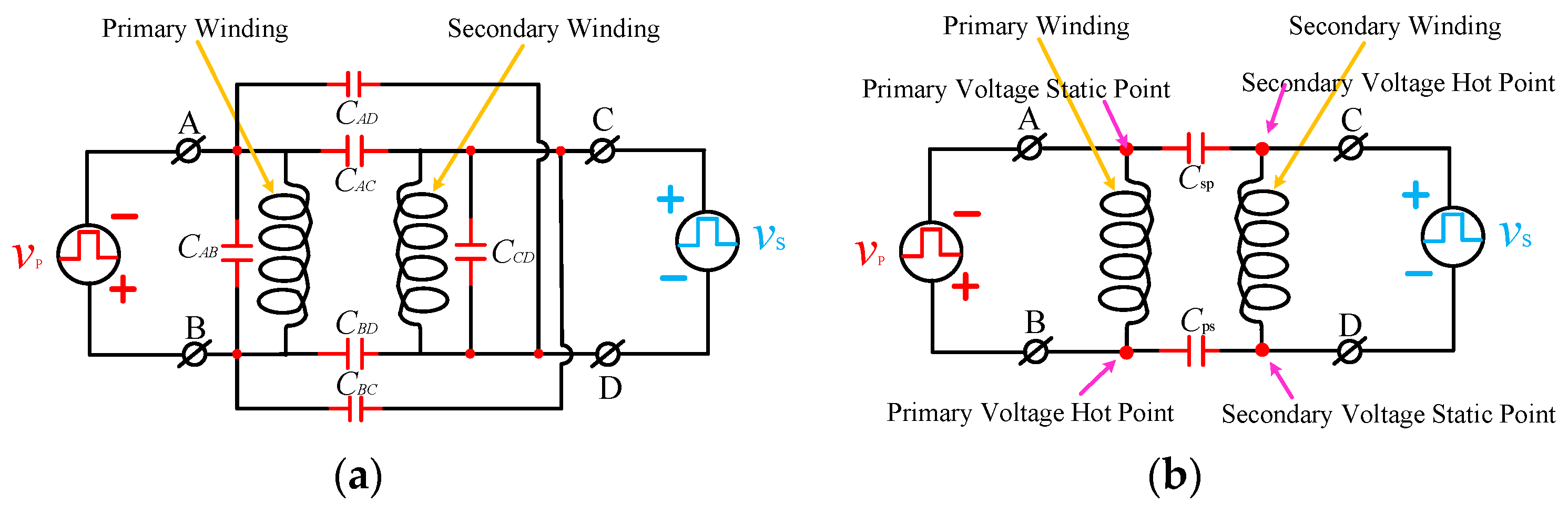
2. Lumped Capacitance Model of the Transformer

2.1. Transformer CM Noise Model

Many previous references have proposed the CM noise model of the transformer. As shown in Figure 2a, for four terminals of a transformer there are six equivalent lumped capacitances [12]. CAB and CCD represent the intrawinding capacitance, which has nothing to do with the CM displacement current conduction between primary and secondary and can be neglected in the CM noise model. The voltage potential of terminals A, B, C, and D are defined as VA, VB, VC, and VD, respectively. The displacement current flowing through the interwinding capacitance CAC, CBD, CBC, and CAD can be calculated by
i T r a n s = C A C d ( V A V C ) d t + C B D d ( V B V D ) d t + C B C d ( V B V C ) d t + C A D d ( V A V D ) d t = ( C A C + C A D ) d V A d t + ( C B D + C B C ) d V B d t ( C B C + C A C ) d V C d t ( C B D + C A D ) d V D d t
In a flyback topology, the winding connection is shown in Figure 2a. Points B and C are voltage hot points, which are connected to the primary MOSFET and the secondary diode, respectively. Points A and D are voltage static points, which are connected to the primary ground and the secondary ground, respectively. Because points A and D will not generate dv/dt, the expression (1) can be further simplified as (2):
i T r a n s = ( C B C + C B D ) d V B d t ( C B C + C A C ) d V C d t
There are three lumped capacitances—CBC, CBD, and CAC—to determine the displacement current flowing through transformer coupling path. To further simplify the expression (2), CBC + CBD and CBC + CAC are defined as Cps and Csp, respectively. For flyback topology with three-wires (L, N, and GND wires), the voltage difference between the primary ground (PG) and the secondary ground (SG) can be omitted due to the small voltage drop on LISN. For flyback topology with two-wires (L and N wires), the voltage difference can also be neglected if the parasitic capacitance Csg between the secondary ground and the ground is far larger than CQ (CQ is the equivalent lumped capacitance of the transformer and it will be introduced in Section 4). The CM current flowing through the transformer can be expressed as
i T r a n s = C ps d V B d t C sp d V C d t
where Cps is an equivalent lumped capacitance, which represents that the primary CM noise source generates CM current flowing through Cps to the secondary side. It is connected between the primary voltage hot point and the secondary static point. Similarly, Csp represents that the secondary CM noise source generates CM current flowing through Csp to the primary side.
Figure 2b depicts the transformer winding two-capacitance model. Here, ips is defined as Vp*Cps and isp is defined as Vs*Csp. If ips is equal to isp, the CM current flowing through transformer will have the opportunity to be totally canceled due to their same amplitudes and opposite phases.

2.2. CM Noise Circuit Model

Figure 3a is the CM noise circuit model of the flyback converter when the diode is used in the secondary side. It can clearly find that the CM current isp is antiphase with ips and ipg. It is possible to make a balance among isp, ips, and ipg. ipg is the displacement current flowing through parasitic capacitance between the drain of the primary MOSFET and the ground. Figure 3b show the CM noise circuit model of the flyback converter when the MOSFET is used in the secondary side. The phase of the secondary CM noise source has inversed if the secondary MOSFET is located in the secondary ground to simplify its gate driving. It is impossible to make a balance among isp, ips, and ipg. In order to improve this situation, an antiphase winding is added between the adjacent primary and secondary windings to generate an antiphase CM displacement current to cancel isp and ips. Z1–Z6 represent the parasitic parameters of the CM noise conduction paths. n and n1 are the turn ratio between the primary winding and the secondary winding and between the primary winding and the antiphase winding, respectively.

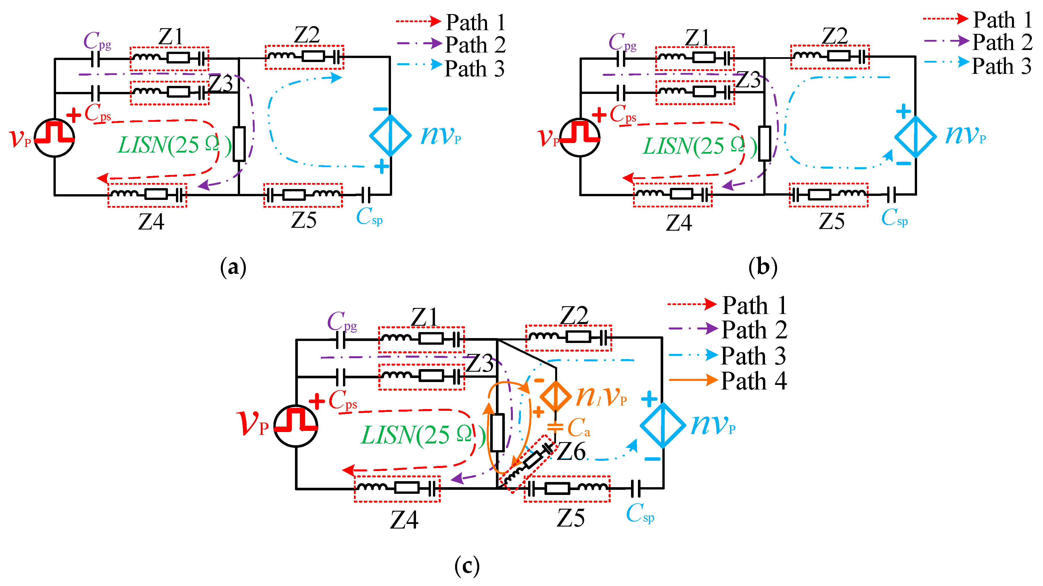
3. Calculation of the CM Displacement Current Flowing through Transformer Coupling Path

Figure 4a–c shows the transformer winding structure with the different winding arrangements. Various kinds of winding arrangements are proposed in previous references for some particular considerations. For instance, the transformer with interleaved winding structure can afford the minimal winding loss at the cost of large interwinding capacitance, which will worsen EMI characteristic. The transformer with PS ( primary secondary) winding structure can lower the EMI characteristic but this action will sacrifice the efficiency of the converter. For calculating the CM displacement current flowing through the inerwinding capacitance of the transformer, it should be noticed that only the displacement current flowing through the adjacent primary and secondary winding can be called CM noise current. Hence, the following will introduce the basic method of calculating the displacement current flowing through transformer coupling path under different winding arrangements.
It is assumed that the turn number of windings Wp1, Wp2, Wp3, Wp4, Ws1, and Ws2 are Np1, Np2, Np3, Np4, Ns1, and Ns2, respectively. Hence, the voltage potential distribution along each turn can be expressed as follows. The voltage differences between two terminals of the primary winding, and between two terminals of the secondary winding are defined as vp and vs, respectively. They should satisfy
v p v s = N p N s = N p 1 + N p 2 + N p 3 + N p 4 N s 1 + N s 2
{ v p = v B v A v s = v D v C
where vA, vB, vC, and vD are the voltage potentials of the primary and secondary winding terminals.
It is assumed that the voltage potential distribution along each winding is evenly and linearly distributed. The reason why the voltage potential varies linearly along the winding is that the effect of leakage inductance, the skin effect, and the proximity effect are ignored. The expressions of the voltage potential distribution of each layer are as follows.
v p 1 ( x ) = v p N p N p 1 x h + v A
v p 2 ( x ) = v p N p N p 2 x h + v p N p ( N p 1 + N p 2 ) + v A
v p 3 ( x ) = v p N p N p 3 x h + v p N p ( N p 1 + N p 2 ) + v A
v p 4 ( N pi ) = v p N p N p 4 x h + v B
v s 1 ( N pi ) = v s N s N s 1 x h + v C
v s 2 ( N pi ) = v s N s N s 2 x h + v D
The structure capacitance, Cstr, can be approximated as a plate capacitor to calculate its capacitance. Reference [15] deduced the accurate formula:
C s t r = 2 π ε o ε r h ln ( d 1 / d 2 ) , d 1 d 2 < < h
where ε0 is the permittivity of the vacuum and εr is the relative permittivity of the dialect between the two adjacent winding layers. d1 and d2 are the distance between the primary (secondary) and the center column of the magnetic core.

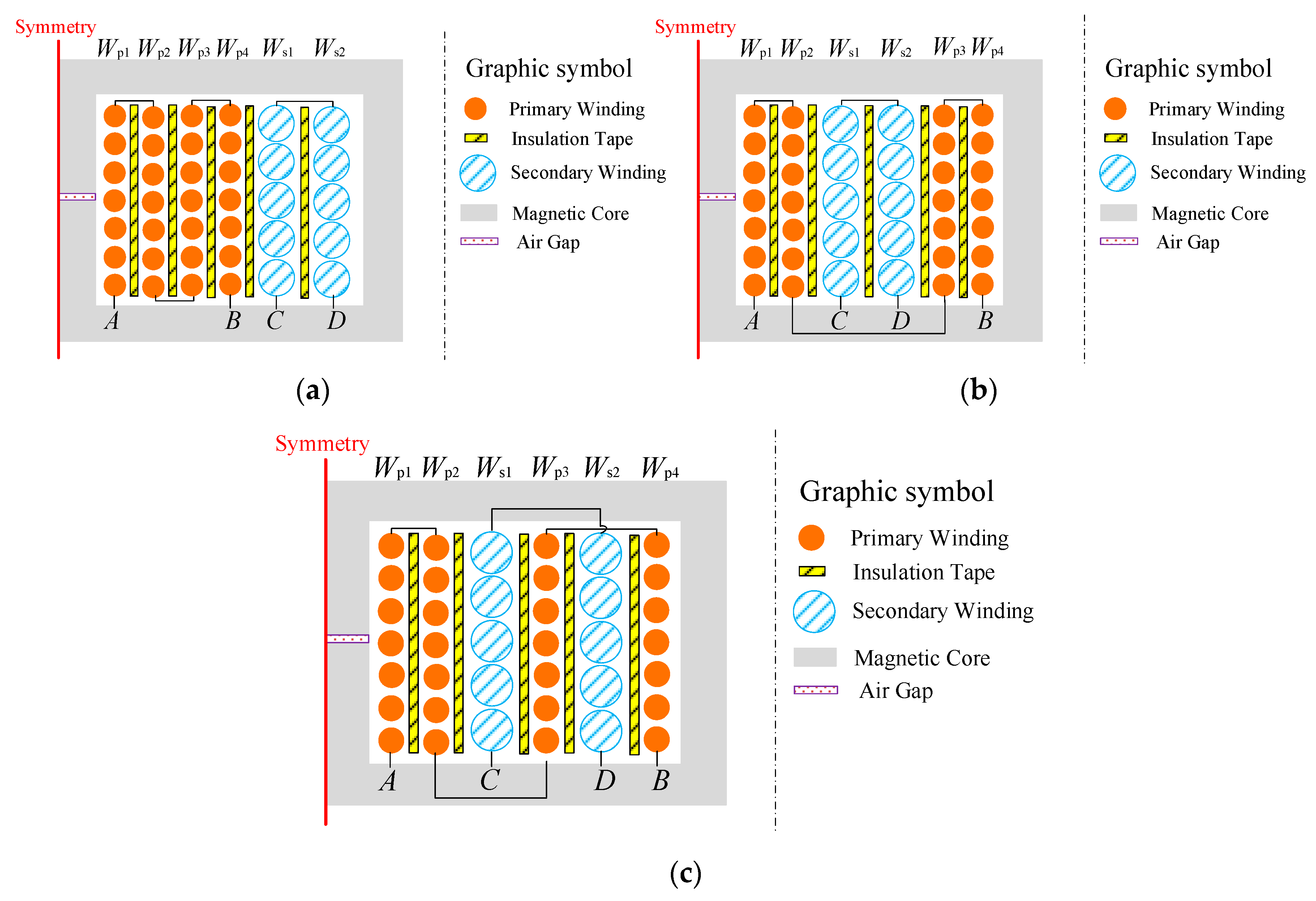
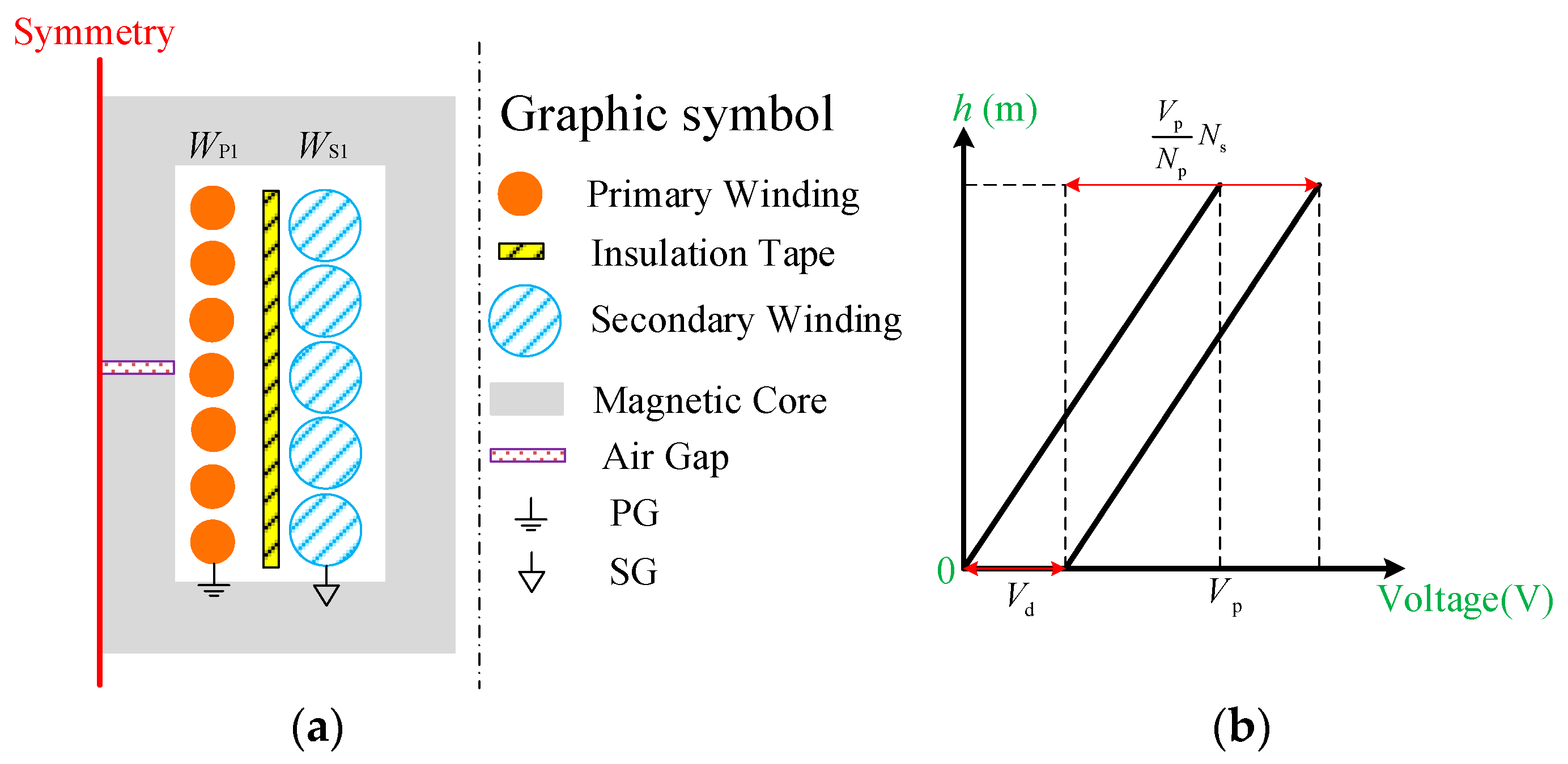
3.1. PS Winding Arrangement

Figure 4a shows a transformer winding structure under PS arrangement. For calculating the CM displacement current iCM_dis under a PS winding arrangement, calculating the displacement current between the layers Wp1 and Ws1 is enough. Then, the CM displacement current iCM_dis is
i CM _ dis = d Q P 4 S 1 d t = d d t 0 h C p 4 s 1 h ( v p 4 ( x ) v s 1 ( x ) ) d x = C p 4 s 1 d d t { 1 2 ( v p N p N p 3 + 2 v B ) 1 2 ( v s N S N S 1 + 2 v C ) }
where Cp4-s1 is the structure capacitance between the adjacent layers P4 and S1 that can be calculated according to (12).

3.2. Sandwich Winding Arrangement

Figure 4b shows a transformer winding structure under the sandwich structure. The CM displacement current between adjacent primary and secondary winding is represented by ip2s1 and ip3s2. Then, the total CM displacement current is
i CM _ dis = d d t ( Q P 2 S 1 + Q P 3 S 2 ) = d d t ( 0 h C p 2 s 1 h ( v p 2 ( x ) v s 1 ( x ) ) d x + 0 h C p 3 s 2 h ( v p 3 ( x ) v s 2 ( x ) ) d x ) = d d t { 1 2 C p 2 s 1 ( ( v p N p ( 2 N p 1 + N p 2 ) + 2 v A ) ( v s N s N s 1 + 2 v C ) ) + 1 2 C p 3 s 2 ( ( v p N p ( 2 N p 1 + 2 N p 2 + N p 3 ) + 2 v A ) ( v s N s N s 1 + 2 v D ) ) }
where Cp2-s1 and Cp3-s2 are the structure capacitance between adjacent layers P2 and S1 and between layers P3 and S2 that can be calculated according to (12).

3.3. Interleaved Winding Arrangement

Figure 4c shows a transformer winding structure under interleaved structure. The CM displacement current between the adjacent primary and secondary winding are ip2s1, ip3s1, ip3s2 and ip4s2. Then, the total CM displacement current is
i CM _ dis = d d t ( Q P 2 S 1 + Q P 3 S 1 + Q P 3 S 2 + Q P 4 S 2 ) = d d t { C p 2 s 1 h ( v p 2 ( x ) v s 1 ( x ) ) d x + 0 h C p 3 s 1 h ( v p 3 ( x ) v s 1 ( x ) ) d x + C p 3 s 2 h ( v p 3 ( x ) v s 2 ( x ) ) d x + 0 h C p 4 s 2 h ( v p 4 ( x ) v s 2 ( x ) ) d x } = d d t { 1 2 C p 2 s 1 ( ( v p N p ( 2 N p 1 + N p 2 ) + 2 v A ) ( v s N s N s 1 + 2 v C ) ) + 1 2 C p 3 s 1 ( ( v p N p ( 2 N p 1 + 2 N p 2 + N p 3 ) + 2 v A ) ( v s N s N s 1 + 2 v C ) ) + 1 2 C p 3 s 2 ( ( v p N p ( 2 N p 1 + 2 N p 2 + N p 3 ) + 2 v A ) ( v s N s N s 1 + 2 v D ) ) + 1 2 C p 4 s 2 ( ( v p N p ( N p 4 ) + 2 v B ) ( v s N s N s 1 + 2 v D ) ) }
where Cp2-s1, Cp3-s1, Cp3-s2 and Cp4-s2 are the structure capacitance between adjacent layers P2 and S1, layers P3 and S1, layers P3 and S2, and layers P4 and S2, respectively. They can be calculated according to (12).
According to (13)–(15), it can find that the CM displacement current is generated due to the existence of the voltage potential distribution along with the adjacent primary and secondary winding. Only the displacement current flowing through the adjacent primary and secondary winding can contribute to forming the CM current. The essence of the CM displacement current is the electric charge induced in the secondary side. Hence, if the average voltage potential distributions along the primary and secondary winding are equal, there is no CM charge induced in the secondary side.

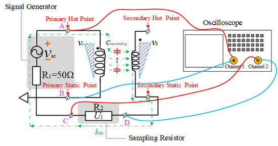
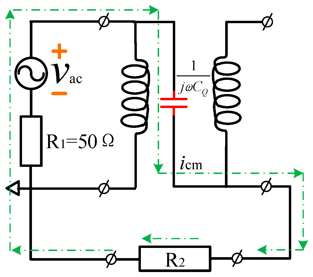
4. Evaluation Method of the Transformer

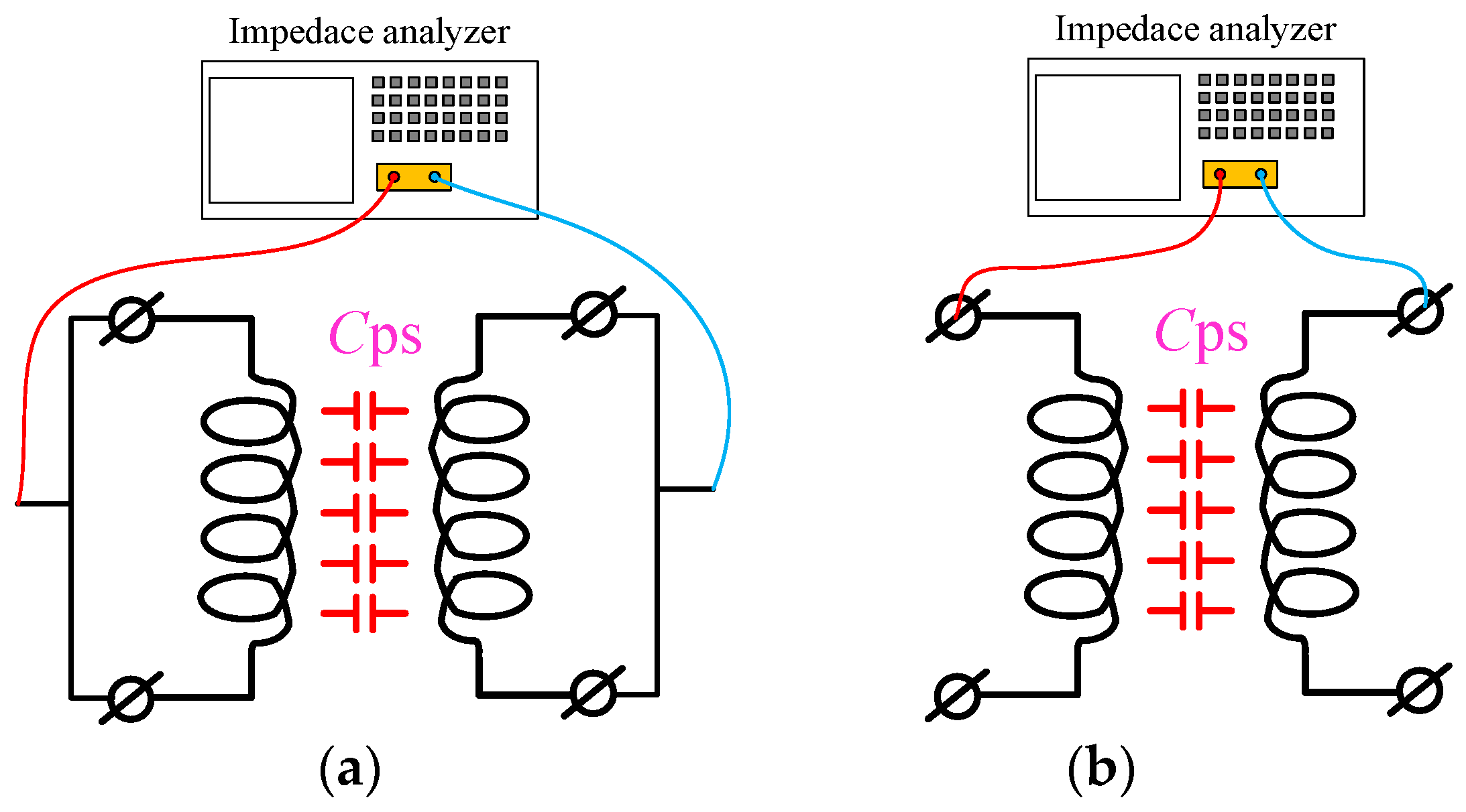
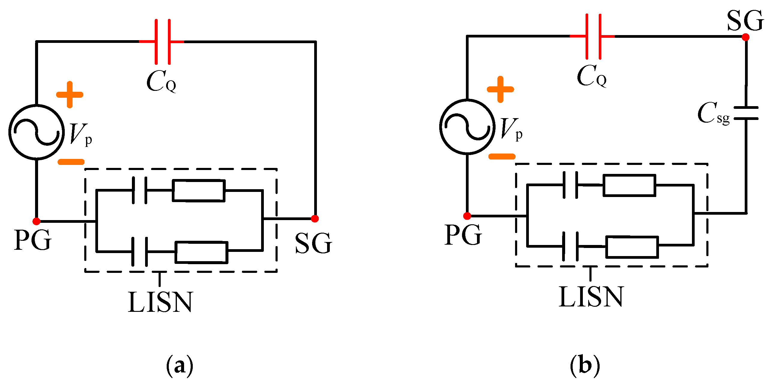
4.1. Previous Evaluation Method

Many previous references also have discussed the issue on how to evaluate the CM noise behavior of the transformer [17,18,19,20]. Figure 5a,b depicts the traditional transformer CM characteristic evaluation method. Using impedance analyzer to measure the CM capacitance of the transformer is impractical. Because this method will not make the primary and the secondary winding build the voltage potential distribution along each winding, and this method can only measure the structure capacitance of the transformer. According to (13)–(15), it can find that the CM displacement current is both related to the structure capacitance between adjacent primary and secondary winding layers and the voltage potential distribution of the winding; merely measuring the structure capacitance cannot effectively reflect the CM displacement current characteristic of the transformer. As have discussed above, the CM noise in transformer coupling path is formed by the voltage potential distribution. Therefore this method cannot totally represent the conductive CM noise behavior of the transformer.
In order to take the voltage potential distribution along with the winding into consideration, reference [19], proposed using an EMI receiver (spectrum analyzer, network analyzer) with a TG option to measure the insertion loss (IL) in order to evaluate the transformer as shown in Figure 6. The positive terminal of the TG is connected to voltage hot point of the primary side and the ground terminal of TG is connected to the primary voltage static point. TG will output sinusoidal signal assigned on the primary winding, and its amplitude is 1 V. Then, the secondary winding will form the voltage potential distribution along with each turn. In this method, the transformer is regarded as a pure capacitance to conduct CM noise. The CM displacement current will flow through this equivalent CM noise capacitance and generate voltage drop in resistor R2, as shown in Figure 6b. Resistor R2 is located in the RF input terminal. Based on the definition of the insertion loss, a lumped equivalent capacitance CQ can be calculated to evaluate the CM noise characteristic of the transformer, according to (16).
C Q = 1 2 π f 10 40 I L 10 10 4
This method is very effective to evaluate the CM noise behavior of the transformer in low-frequency range since the capacitive coupling contributes more in low-frequency range, and for higher frequency range inductive coupling is a major factor for conductive CM noise. However, the main drawback of this method is that needs expensive test instruments (EMI receiver with TG option or spectrum analyzer with TG option). Many transformer manufacturers do not have enough money to afford these professional instruments. Besides, precise calibration of these professional instruments is also needed, which complicates the measurement process. Reference [21] proposed using numerical algorithms to achieve parameter extraction and parameter identification of the transformer. Besides, some numerical methods for transformer evaluation in [9,22] have been proposed to design wire-wound transformers. However, these evaluation methods are based on the finite element method (FEM) commercial simulation software, i.e., Ansys Maxwell which is too expensive to be purchased by some transformer manufactures.

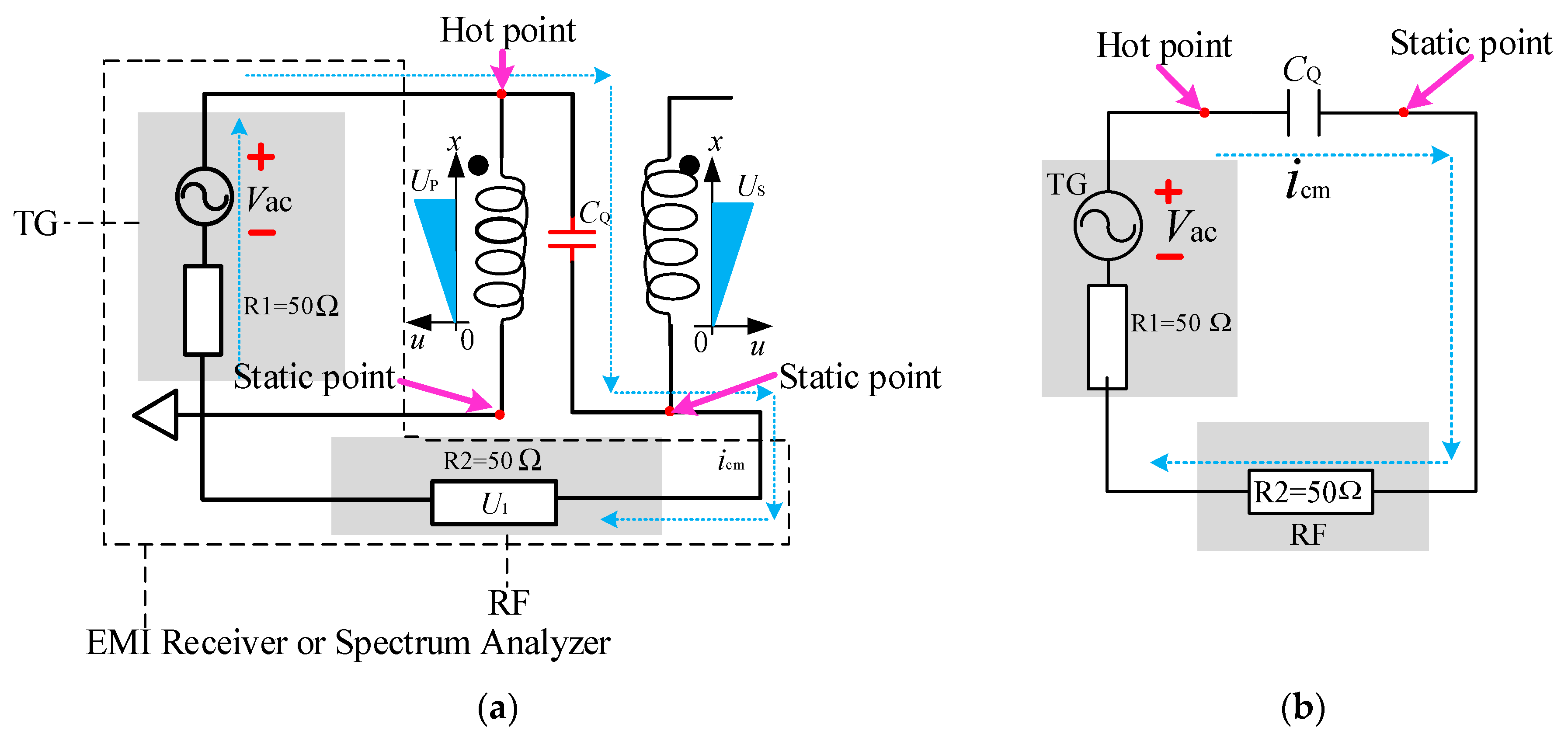
4.2. Proposed Evaluation Method

Based on the above considerations, this paper proposes a practical CM noise characteristic evaluation method to achieve the same evaluation effect as discussed above. Only a signal generator and an oscilloscope can achieve the same evaluation effect in low-frequency EMI noise as shown in Figure 7. The positive terminal of the signal generator is connected to the primary voltage hot point and the ground terminal of the signal generator is connected to both primary voltage static point and one terminal of R2. The other terminal of R2 is connected to the secondary voltage static point. The secondary voltage hot point is open. In this measurement process, the CM displacement current flows through the distributed CM coupling capacitance Cinterwinding between the adjacent primary and secondary layers and generates a voltage drop in resistor R2. For transformers with different winding arrangements, the CM displacement current flowing through the transformer will be different. Then, the voltage drop measured by voltage probe in Channel 2 of the oscilloscope can reflect the size of the CM displacement current flowing through the transformer.

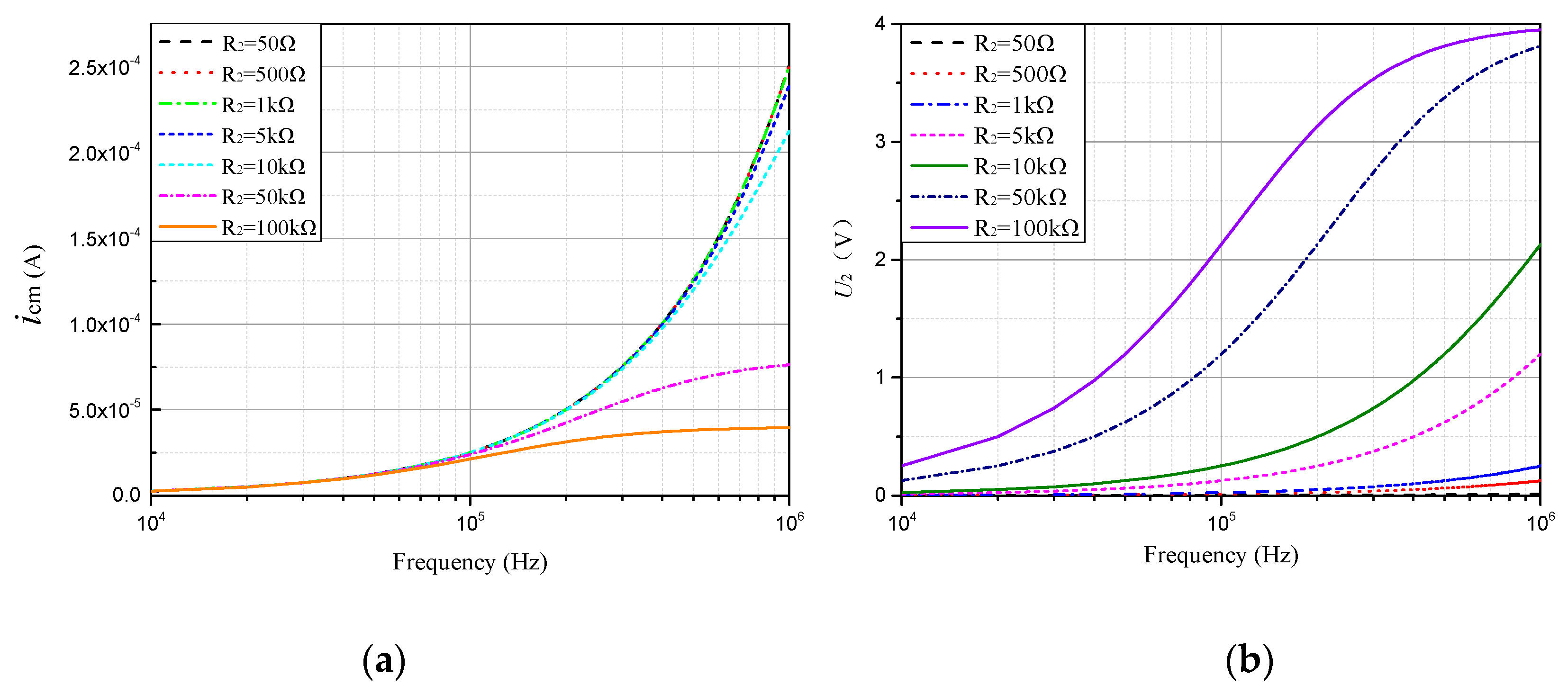
4.2.1. Selection of Resistor R2

It seems that the evaluation methods of the EMI receiver with TG option and the signal generator are the same. However, there is a significant difference in the selection of the resistance of R2 that will be analyzed in detail in the following.
The EMI receiver with TG option and the network analyzer are high-precision instruments for measuring small signals. Its sampling resistor R2 depicted in Figure 6a uses precision noninductive resistance, which means that the resistor component R2 can be regarded as pure resistance. Then, the impedance will remain unchanged equaling to 50 Ω as the frequency increases. The EMI receiver and network analyzer are both used in conductive EMI noise frequency ranges (150 KHz–30 MHz) due to the EMI test standard of the switch-mode power supplies (SMPSs). The insertion loss (IL) and S parameters can be measured by these instruments. Hence, the tiny voltage drop in resistor R2 can be precisely measured due to its high precision. However, if the same resistance is used for resistor R2 in the proposed evaluation method to sample the CM noise voltage, it will be impractical. That is because the size of the CM noise displacement current is extremely tiny, which is at the level of microampere. Then, the voltage drop in R2 is tiny, which cannot be precisely measured by the voltage probe. Hence, choosing a proper resistance is critical in the proposed evaluation method.
The distributed CM coupling capacitance of the transformer is represented as a lumped capacitance CQ for simplifying the analysis. Figure 8 shows the equivalent circuit of the proposed evaluation method. The CM displacement current icm flowing through the lumped equivalent capacitance CQ can be expressed as
i cm = v ac R 1 + R 2 + 1 j ω C Q
The voltage drop U2 in sampling resistor R2 is
U 2 = v ac R 1 + R 2 + 1 j ω C Q R 2
In order to represent the variation tendency of the CM displacement current icm and the voltage drop U2 in resistor R2 versus the resistance of R2, the capacitance of CQ will be assumed to be a certain value. For different value of CQ, the basic variation tendencies of icm and U2 are almost the same. In the analysis, it is assumed as 10 pF. The root mean square (RMS) of Vac is 4 V. Then, the size of the CM displacement current icm and the voltage drop U2 can be calculated under different frequencies. For general isolated SMPS, its switch frequency is from 10 kHz to 1 MHz, and a switching frequency will be chosen as signal excitation frequency to evaluate the transformer. Figure 9a,b shows the frequency-dependent curve of icm and U2. Figure 9a shows that the larger resistance of R2 will cause less displacement current icm for the same transformer. Figure 9b shows that larger resistance of R2 will cause a larger voltage drop in itself. If the resistance of R2 is equal to 50 Ω, the voltage drop in R2 will be too tiny to be precisely measured. Therefore, the resistor with 50 Ω is impractical for use in this evaluation method due to the limitation of probe accuracy. In order to acquire a larger voltage drop in R2, the effective implementation is to increase the resistance of R2 to sample the larger voltage. The voltage drop in R2 will increase if the resistance of R2 is increased. However, if the resistance of R2 is too large, it will also be unreasonable
For larger resistance of R2, the voltage difference between the primary ground and the secondary ground will change. The voltage potential distribution of the secondary winding will change versus R2 resistance, and the value of the lumped CM capacitance of the transformer can change. The following will analyze the influence of R2 resistance on the lumped equivalent capacitance CQ in detail.
A transformer with a single layer of the primary and the secondary winding is used to illustrate this phenomenon, as shown in Figure 10a. Figure 10b shows the voltage potential distribution of the primary and secondary winding and their expression can be given as follows
v p ( x ) = V p h x
v s ( x ) = V p N p N s x h + V d
where Np and Ns are the turns of the primary and secondary winding, respectively. Vd is the voltage difference between the primary ground and the secondary ground. h is the height of the core window.
According to (19) and (20), the dynamic CM capacitance CQ can be calculated as
C Q = Q V p = 1 V p C 0 h 0 h ( v p ( x ) v s ( x ) ) d h = 1 2 V p C 0 { V p ( V p N p N s + 2 V d ) } = 1 2 C 0 { 1 N s N p } 1 2 C 0 2 V d V p
From (21), it can be found that the dynamic CM capacitance CQ is not only determined by the structure capacitance C0 and the terminal connection of winding, but also determined by the voltage potential difference Vd between the primary ground and the secondary ground.
The essential reason for this phenomenon is that Vd changes the voltage potential distribution of the secondary winding and the resultant electric charges induced in the secondary side can also be changed. Hence, the resistance of R2 should be chosen appropriately.

4.2.2. Ground Potential Difference

For isolated converters with three wires (L, N, and GND lines), the secondary ground is directly connected to ground. This means the voltage difference between the primary ground and the secondary ground is just the voltage drop in LISN by common-mode noise, as shown in Figure 11a, if the voltage drop of the rectifier bridge is ignored. Obviously, the voltage drop in LISN is usually very small, compared with the voltages of the primary and secondary noise sources, i.e., the voltages of primary MOSFET and secondary MOSFET. Therefore, the potential difference between the primary ground and the secondary ground can be omitted when the isolated converter has three wires. In this kind of circuit configuration, the resistance chosen for R2 should be as small as possible, and the voltage drop in R2 should be maintained so that it can be precisely measured.
For isolated converters with two-wires (L and N wires), the secondary ground is floating. So the voltage drop between the primary ground and the secondary ground is determined by both the value of CM current and the parasitic capacitance Csg between the secondary ground and ground as shown in Figure 11b. In this case, whether the voltage difference between the primary ground and the secondary ground can be ignored or not depends on the value comparison of Csg and CQ. If CQ is much smaller than Csg, the voltage difference between the primary ground and the secondary ground can be regarded as 0. If the condition mentioned above cannot be met, the accuracy of the proposed method will be affected. However, the transformer CM coupling path is one of the major CM noise conduction paths. Eliminating the CM noise flowing through transformer coupling path can significantly lower the CM noise of the whole converter. When the designed transformer can achieve zero CM noise in transformer coupling path, the voltage difference between the primary ground and the secondary ground can be omitted. Hence, when the isolated converter is with two wires, the proposed method still can precisely evaluate the transformer with the minimum value of the CM noise. Therefore, the resistance of R2 should be chosen as small as possible.
Based on the above discussion, the resistance of sampling resistor R2 should be chosen appropriately. If the resistance of sampling resistor R2 is too small it can lead to a small voltage drop in R2, which cannot be precisely measured by the voltage probe. If the resistance is too large it can lead to a large voltage drop in R2, which will change the voltage potential distribution of the secondary winding and the lumped equivalent capacitance of the transformer will be changed at the same time. It should be pointed out that the main drawbacks and limitations of the proposed evaluation method are that it can only effectively evaluate low-frequency CM noise behaviors of the transformer. Because the transformer is regarded as a pure capacitance to conduct CM noise in the proposed evaluation method the capacitive coupling plays a major role in low-frequency CM noise conduction. In the high-frequency range, both capacitive and inductive coupling will make a difference in high-frequency CM noise and the transformer cannot be regarded as a pure capacitance to conduct CM noise. Besides, the proposed evaluation method may not be applicable to do further analysis in high-frequency CM noise compared with the previous methods with EMI receiver and network analyzer. That is due to the accuracy of the test instrument. Higher frequency CM noise suppression can be solved by the design of the CM EMI filter.

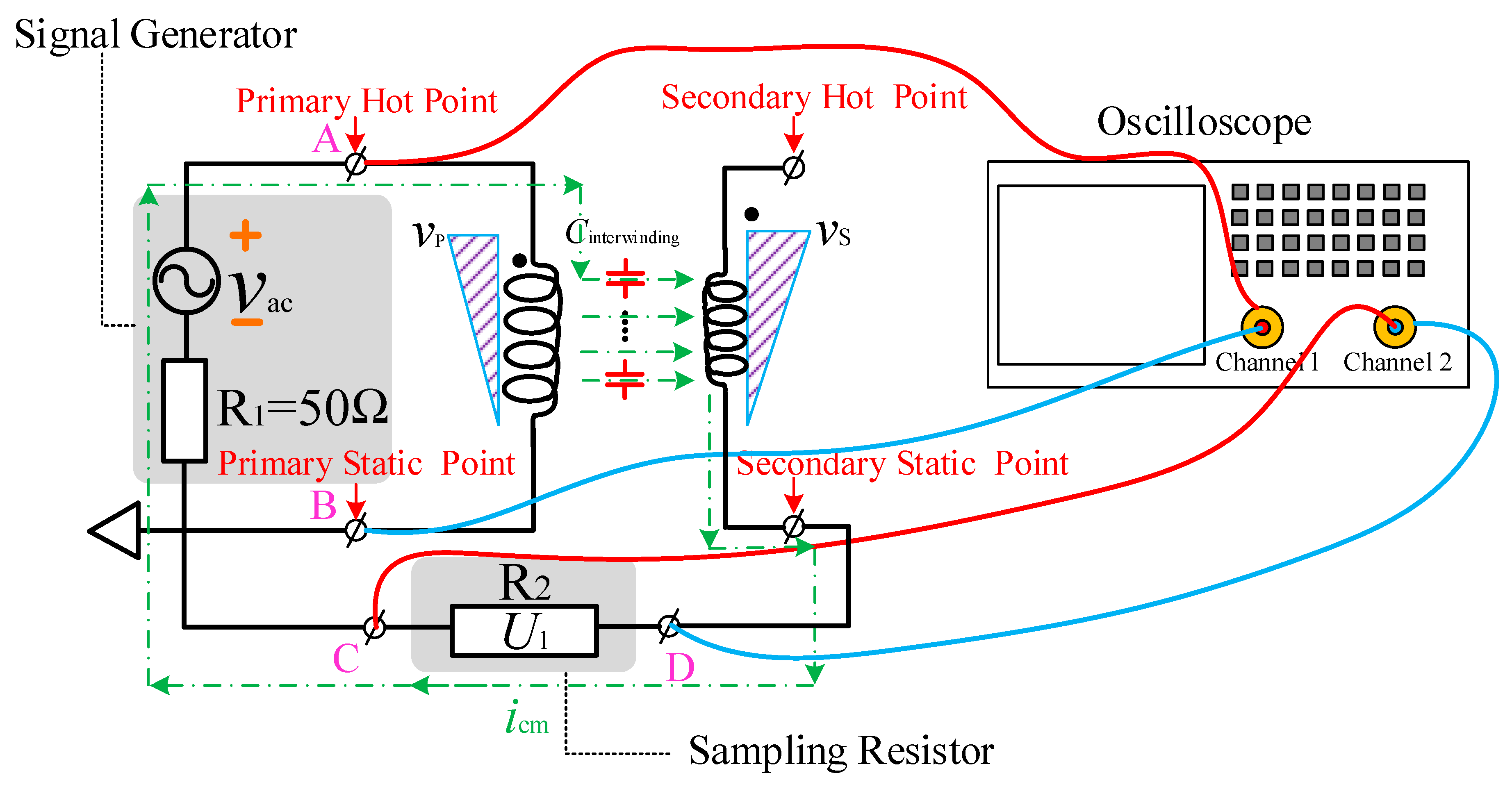
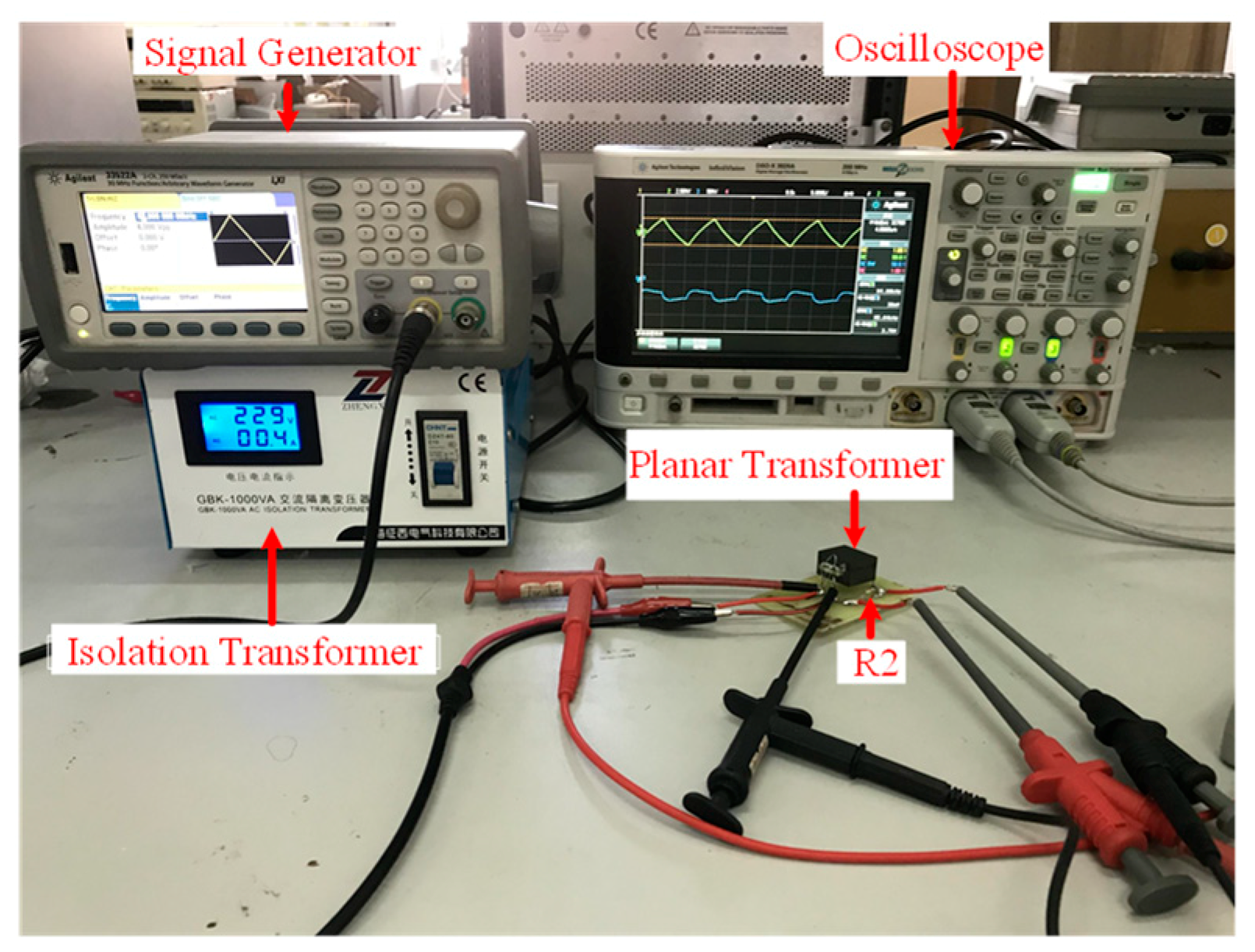
5. Experimental Results

In order to verify the effectiveness of the proposed evaluation method, a flyback converter prototype with the different winding arrangement of the PCB planar transformer is used to verify. The secondary side of the designed transformer is connected to MOSFET to achieve synchronous rectification and its detailed circuit specification is shown in Table 1. The designed flyback adapter has three wires.
There are three planar transformers with different turns of the compensation winding. They are labeled as 1#, 2#, and 3#, respectively. For 1#, 2#, and 3# transformers, the turns of the compensation winding are 8, 10, and 12 turns, respectively. The compensation winding is inserted in between the adjacent primary and secondary windings.
The measurement platform is shown in Figure 12, where the signal generator is Agilent 33522 A and the oscilloscope is Agilent DSO-X3024 A. The differential probe is Agilent N2790 A. As for the selection of the sampling resistor, the basic principles have been discussed in Section 4. Hence, this section will verify the significance of selecting a proper resistance of the sampling resistor. Besides, it is also important to select a suitable signal source applied in the primary winding.

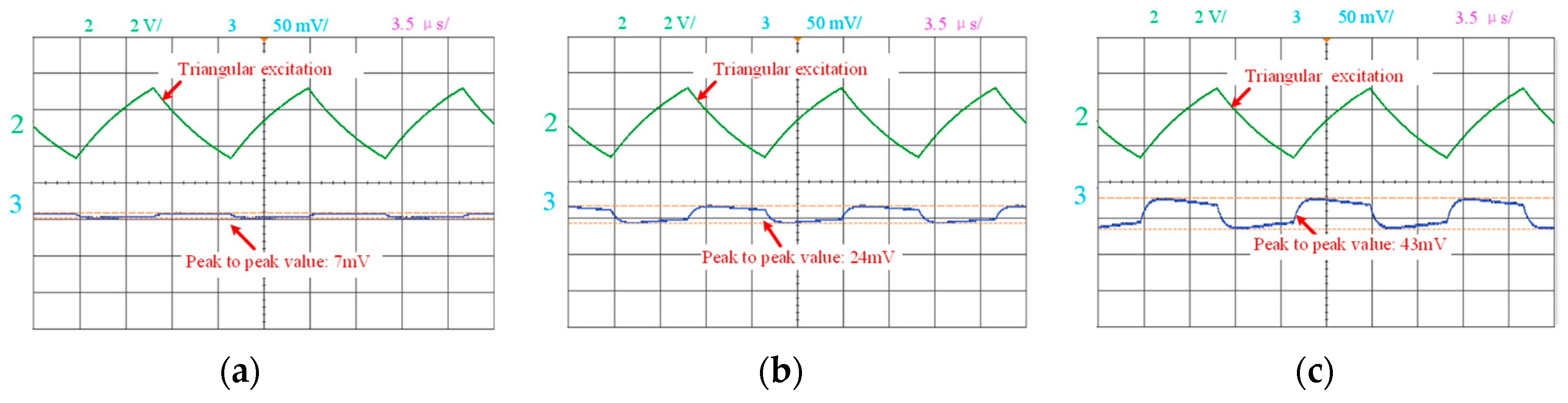
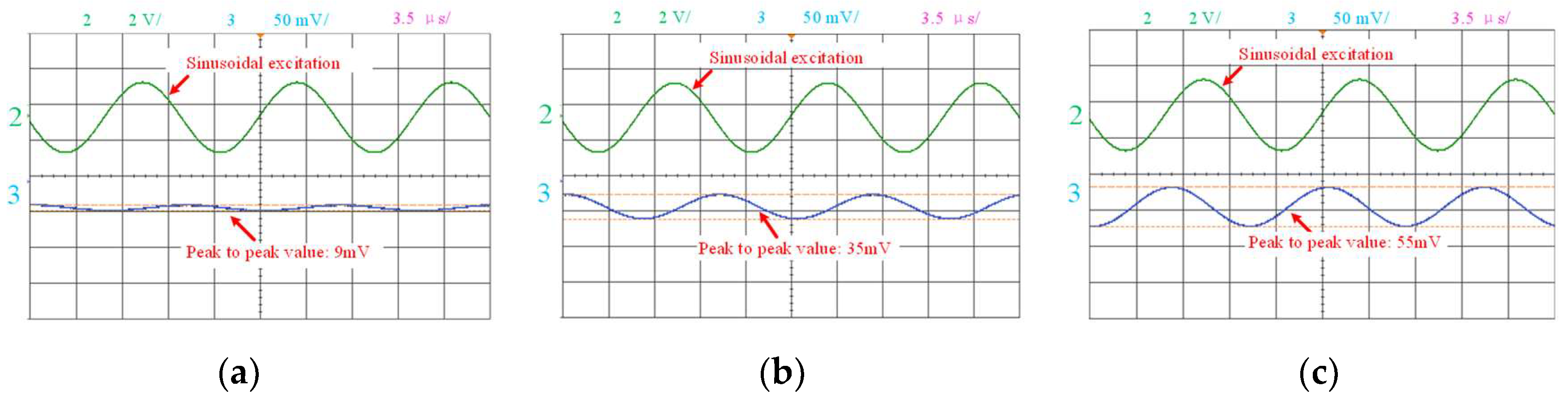
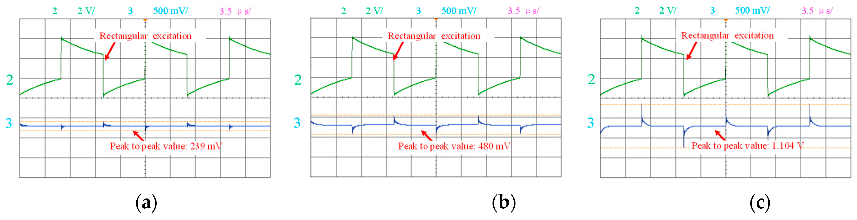
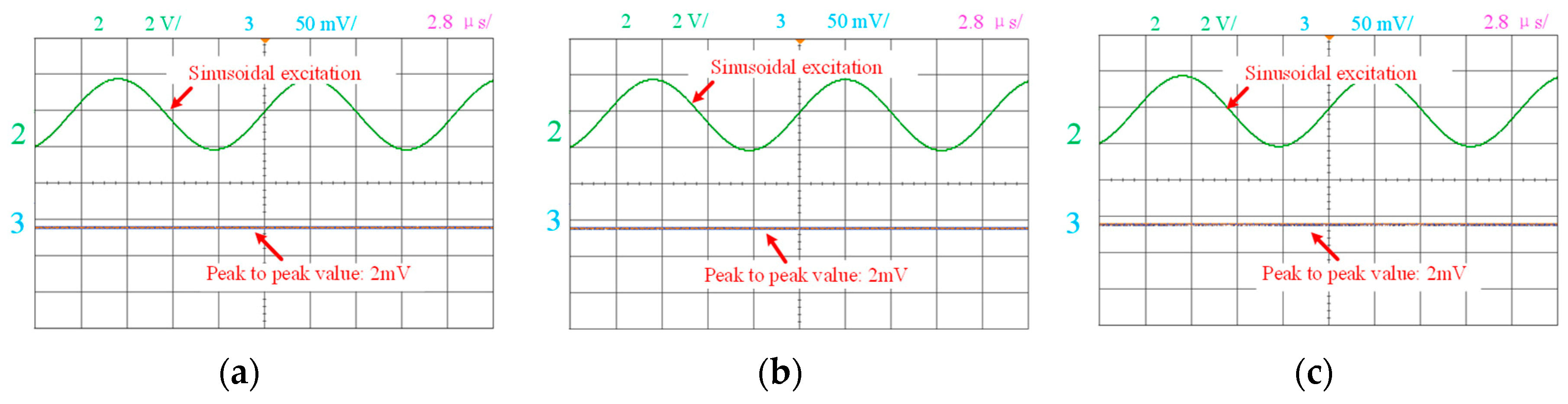
5.1. Measurement Voltage Waveform

The signal generator can output sinusoidal signal, square signal, and triangular signal. As shown in Figure 13, Figure 14 and Figure 15, different kinds of excitation sources are used to evaluate the transformer, respectively. The resistor R2 with 10k Ω is used and the frequency of the signal source is 85 kHz determined by the switching frequency of the converter. The peak-to-peak value of the signal source is 4 V.
Figure 13a–c shows the measurement voltage waveforms of the primary winding and the sampling resistor when the signal generator outputs triangular signal assigned on two terminals of the primary winding. It can find that the triangular signal excitation has been distorted. This phenomenon is due to the power limitation of the signal generator. It is clear that the peak-to-peak value of the voltage in 1# transformer is the minimum and the peak-to-peak value of the voltage in 3# transformer is the maximum. As has been analyzed in Section 4, 1# transformer has the minimum value of CQ, which will lead to the lowest level of CM noise spectrum. However, there is a problem in waveform distortion of the signal source applied in primary winding, which may affect the precision of the evaluation method.
Similarly, Figure 14a–c shows the measurement voltage waveforms of the primary winding and the sampling resistor when the sinusoidal signal is assigned on two terminals of the primary winding. The sinusoidal degree of the signal source is very well compared with that shown in Figure 13. The measurement results are the same as that of using the triangular signal and the sinusoidal signal source does not distort much.
Figure 15a–c shows the measurement voltage waveforms of the primary winding and the sampling resistor when the square signal is assigned on two terminals of the primary winding. It can clearly find that the square signal has distorted severely, which cause the voltage waveform on the sampling resistor to be no longer a standard rectangular wave. There are two peaks in the rising and falling edges of the voltage in R2.
Compared with the experiment results from Figure 13, Figure 14 and Figure 15, the sinusoidal signal source has a minimum distortion degree. Hence, the sinusoidal signal source is recommended as an excitation source to be applied on the primary winding.
Figure 16a–c shows the measurement results of the voltage waveform in sample resistor when the signal generator outputs sinusoidal signal assigned on two terminals of the primary winding. The resistor R2 with 50 Ω is used. It is clear that the peak-to-peak values of the sample voltages in 1#, 2#, and 3# transformers are almost the same. As have been analyzed in Section 4, this phenomenon is duo the tiny CM displacement current flowing through R2, which is out of the minimum measurement scope of the voltage probe. Therefore, the resistor with 50 Ω is impractical to be used in the proposed evaluation method.
From Figure 14, it can be deduced that the 1# transformer has the best ability to suppress CM noise among the three kinds of the transformers.

5.2. CQ Verification

In Section 5.1, three kinds of transformers have been evaluated based on the proposed evaluation method. In this section, the following will use the previous method proposed in [18] to compare the difference between these two methods. Figure 17 shows the measurement results of the insertion loss of 1#, 2#, and 3# transformers. During the capacitive coupling frequency ranges, the transformer can be regarded as a pure capacitance to conduct CM displacement current and the slope of the insertion loss is 20 dB/Dec. For higher frequency range, the capacitive coupling and inductive coupling will make a difference to the insertion loss trace, simultaneously. For 1# transformer, its insertion loss is too small to be precisely measured in the capacitive coupling frequency range, so there is an oscillation in the low-frequency range. In order to calculate its effective capacitance, CQ, it is reasonable to regard it as a straight line in the low-frequency range. Then, using formula (11), the CQ of 1#, 2#, and 3# transformers are calculated as 0.2 pF, 1.8 pF, and 4 pF, respectively. The trend of calculation results conforms well with the evaluation results shown in Section 5.1. In order to further verify the effectiveness of the proposed transformer evaluation method, the following will measure the CM noise spectrums of three kinds of the transformers.

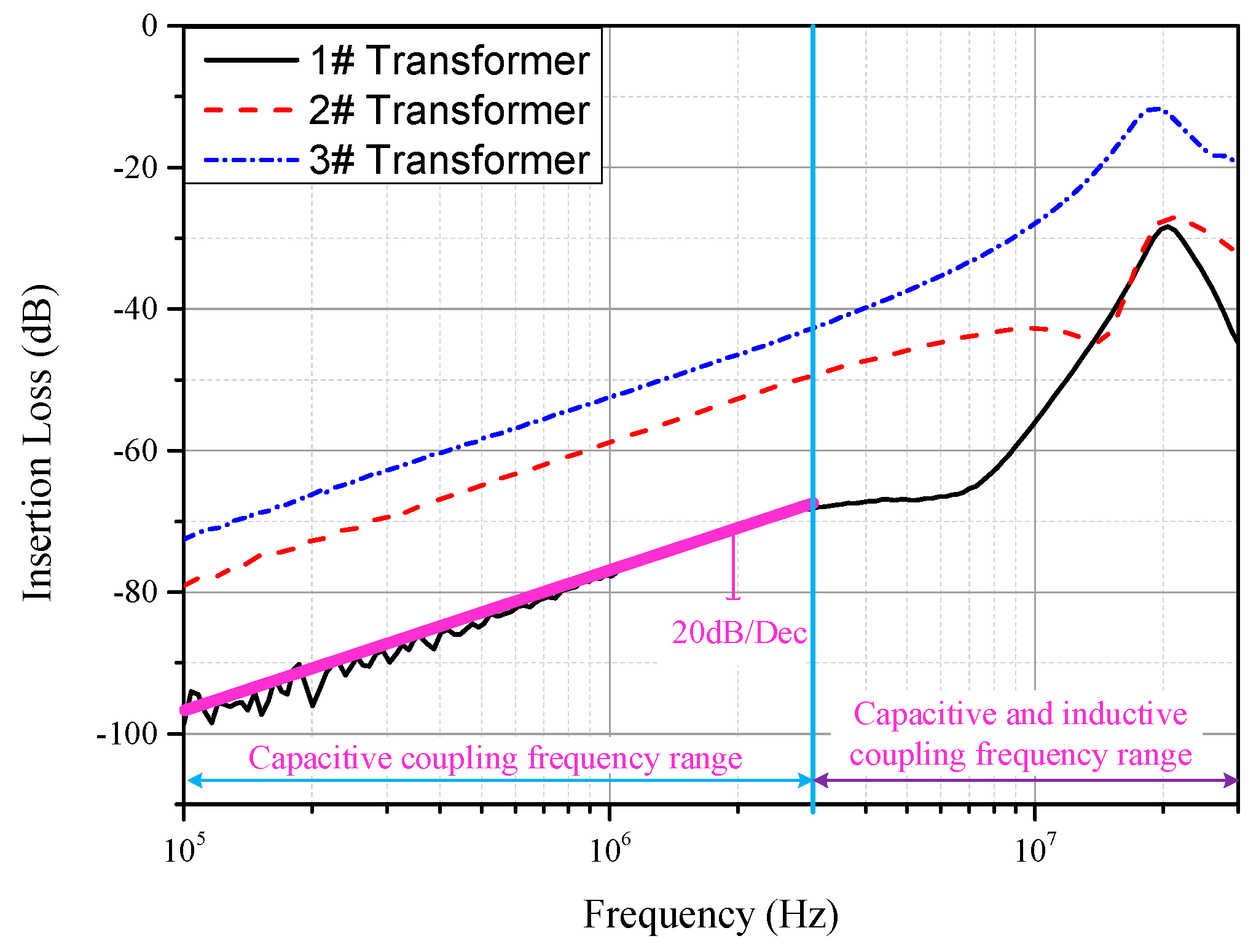
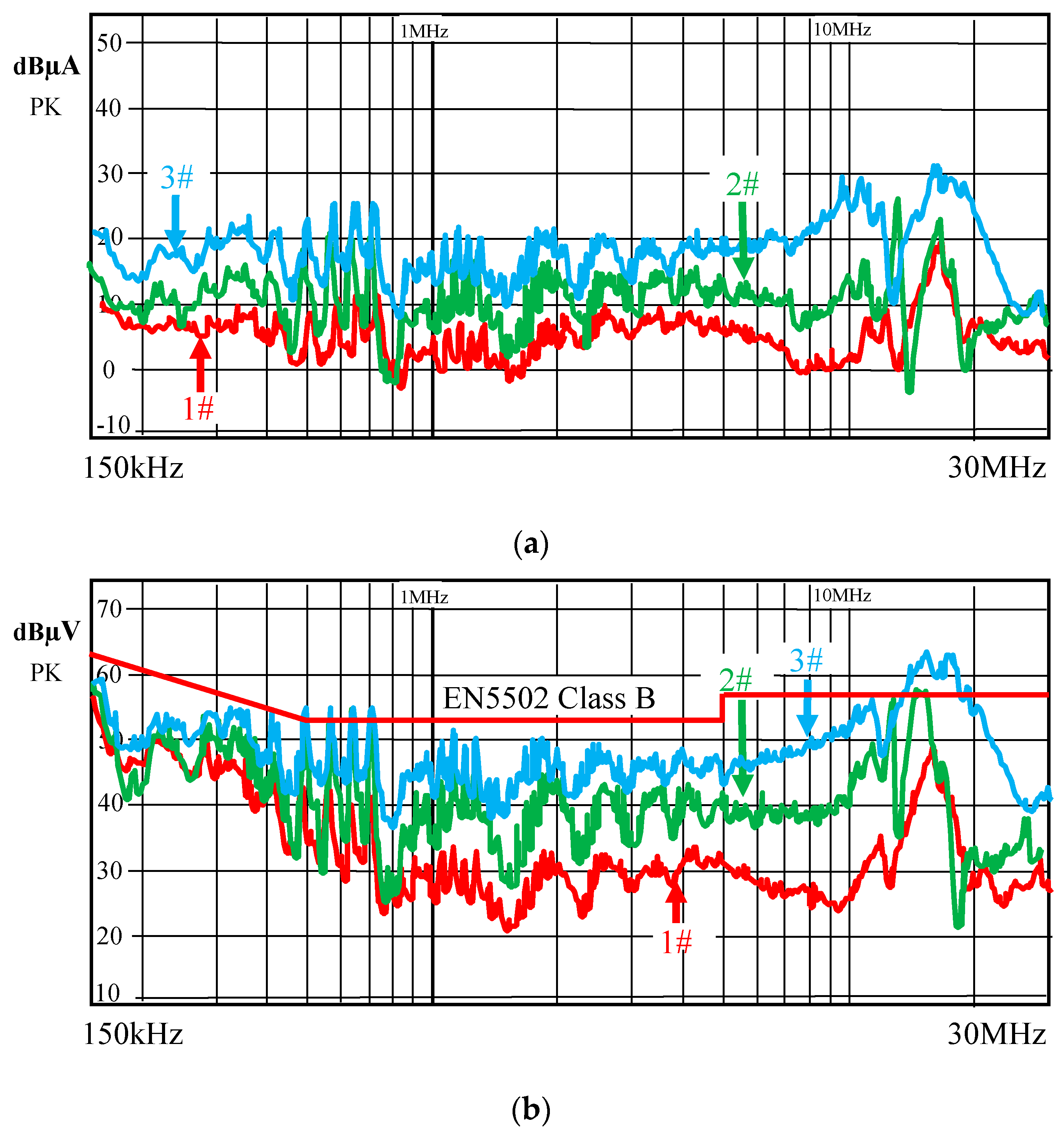
5.3. Noise Spectrum Verification

In order to decouple EMI noise into CM noise and DM noise, the traditional measurement method is to use a noise separator, which is a voltage measurement method. However, the current measurement method is also feasible. For a better and clear understanding, the following will introduce how to use radio frequency (RF) current probe to separate the CM noise from the total EMI noise. Figure 18 shows the CM current measurement method. The CM current flowing through L and N lines are in the same direction. Therefore, using R & S EZ-17 radio frequency current probe can precisely measure the CM current and the measured signal can be transmitted into EMI receiver to be transformed into CM noise spectrum. The test environment is electromagnetic shielding chamber. EMI receiver is R & S ESCI and LISN is R & S ESH2-Z5.
Figure 19a–b shows the EMI noise spectrums of the CM noise spectrum and the total EMI noise spectrum, respectively. In Figure 19a, the flyback converter with 1# transformer can achieve the lowest level of CM noise compared to the 2# transformer and 3# transformer. For higher frequency range (above 17 MHz), the CM noise attenuation effect is not so effective as in low-frequency range due to the complex effects of the parasitic parameter. As shown in Figure 17, the transformer in capacitive and inductive coupling frequency range cannot be regarded as a pure capacitance to conduct CM noise. This is an essential reason for high-frequency CM noise that not easy to be suppressed. In Figure 19b, the reason why the attenuation effect of the EMI noise in the lower frequency range (below 500 kHz) is not so evident is that the EMI noise can be decoupled as CM noise and DM noise. Usually, CM noise contributes more in the higher frequency range, and DM noise also plays a major role in lower frequency range. Transformer winding design can only attenuate the CM noise flowing through transformer coupling path, which has nothing to do with the DM noise attenuation. The proposed method can effectively evaluate the CM noise behavior of the transformer, which is helpful to pass the EMI standard limited line EN55022 Class B.
Figure 20a,b shows the CM noise flowing direction in transformer coupling path when the static points of the primary and secondary winding are shorted together. It can find the CM noise in transformer coupling path will not flow to the ground and be detected by LISN. Hence, this method can verify whether the CM noise has been totally eliminated. This method is impractical to be used in an actual product as this method will make the transformer lose isolation function.
Figure 21 shows the CM noise spectrums when the static points of 1# transformer are shorted. For this situation, the CM current flowing through transformer coupling path will circulate internally instead of being detected by LISN and the measured CM noise spectrums can verify whether the transformer is well designed. It can find that the CM noise spectrum with 1# transformer is almost the same as that with shorting the static points. For this experiment result, it can prove that 1# transformer evaluated by the proposed method has a minimal peak to peak value of the voltage shown in Figure 14. Besides, it also can achieve near zero CM noise flowing through transformer coupling path.
The resistor R2 with 10k Ω is recommended to sample the CM voltage in the proposed method.

6. Conclusions

This paper proposes a general transformer CM noise behavior evaluation method. Only a signal generator and an oscilloscope can come close to achieving the same evaluation effects as in previous references.
This evaluation method has multiple benefits:
  • The measurement instruments are cheaper compared with professional EMI measurement instruments, and many transformer manufactures can easily use this evaluation method.
  • The evaluation method can put the voltage potential distribution of the primary and secondary winding into consideration, which can reflect the CM noise behavior of the transformer.
There are some key parts that should be pointed out:
  • The resistance of R2 should be chosen appropriately.
  • The voltage potential difference between the primary ground and the secondary ground can make a difference to the lumped equivalent CM noise capacitance of the transformer.
  • Sinusoidal signal source is recommended as an excitation to be applied on the primary winding.
  • The proposed evaluation method can effectively evaluate the CM noise behaviors of transformer only in capacitive coupling frequency range.

Author Contributions

Conceptualization: W.C., S.L.; Investigation, Validation, and Formal Analysis: K.F.

Funding

This work was supported by the National Natural Science Foundation of China under Grant 5177036 and the Natural Science Foundation of Fujian Province (2017J01479).

Conflicts of Interest

The authors declare no conflict of interest.

References

  1. Chu, Y.; Wang, S. A generalized common-mode current cancelation approach for power converters. IEEE Trans. Ind. Electron. 2015, 62, 4130–4140. [Google Scholar] [CrossRef]
  2. Limits and Methods of Measurement of Radio Disturbance Characteristics of Information Technology Equipment; European Norm Standard EN 55022; CISPR, European Union: Brussels, Belgium, 2006.
  3. Chu, Y.; Wang, S.; Zhang, N.; Fu, D. A Common Mode Inductor With External Magnetic Field Immunity Low-Magnetic Field Emission and High-Differential Mode Inductance. IEEE Trans. Power Electron. 2015, 30, 6684–6694. [Google Scholar] [CrossRef]
  4. Chan, Y.P.; Pong, M.H.; Poon, N.K.; Liu, C.P. Effective switching mode power supplies common mode noise cancellation technique with zero equipotential transformer models. In Proceedings of the IEEE Applied Power Electronics Conference and Exposition (APEC), Palm Springs, CA, USA, 21–25 February 2010; pp. 571–574. [Google Scholar]
  5. Pentti, L.; Hyvonen, O. Electrically Decoupled Integrated Transformer Having at Least One Grounded Electric Shield. U.S. Patent 7733205 B2, 8 June 2010. [Google Scholar]
  6. Tokaldani, M.A.S.; Shafiei, N.; Ordonez, M. Planar Transformers with Near Zero Common Mode Noise for Flyback and Forward Converters. IEEE Trans. Power Electron. 2017, 32, 2687–2703. [Google Scholar]
  7. Xie, L.; Ruan, X.; Ji, Q.; Ye, Z. Shielding-cancellation technique for suppressing common mode EMI in isolated power converters. IEEE Trans. Ind. Electron. 2015, 62, 2814–2822. [Google Scholar] [CrossRef]
  8. Kong, P.; Wang, S.; Lee, F.C.; Wang, Z. Reducing common-mode noise in two-switch forward converter. IEEE Trans. Power Electron. 2011, 26, 1522–1533. [Google Scholar] [CrossRef]
  9. Chen, H.; Xiao, J. Determination of Transformer Shielding Foil Structure for Suppressing Common-Mode Noise in Flyback Converters. IEEE Trans. Magn. 2016, 52, 1–9. [Google Scholar] [CrossRef]
  10. Bai, Y.; Yang, X.; Li, X.; Zhang, D.; Chen, W. A novel balanced winding topology to mitigate EMI without the need for a Y-capacitor. In Proceedings of the 2016 IEEE Applied Power Electronics Conference and Exposition, Long Beach, CA, USA, 20–24 March 2016; pp. 3623–3628. [Google Scholar]
  11. Cochrane, D.; Chen, D.Y.; Boroyevic, D. Passive cancellation of common-mode noise in power electronic circuits. IEEE Trans. Power Electron. 2003, 18, 756–763. [Google Scholar] [CrossRef]
  12. Duerbaum, T.; Sauerlaender, G. Energy based capacitance model for magnetic devices. In Proceedings of the Sixteenth Annual IEEE Applied Power Electronics Conference and Exposition, Anaheim, CA, USA, 4–8 March 2001; pp. 109–115. [Google Scholar]
  13. Schellmanns, A.; Keradec, J.P.; Schanen, J.L.; Berrouche, K. Representing electrical behavior of transformers by lumped element circuits: A global physical approach. In Proceedings of the IEEE Industry Applications Conference, Phoenix, AZ, USA, 3–7 October 1999; pp. 2100–2107. [Google Scholar]
  14. Besri, A.; Chazal, H.; Keradec, J. Capacitive behavior of HF power transformer: Global approach to draw robust equivalent circuits and experimental characterization. In Proceedings of the IEEE Instrumentation and Measurement Technology Conference (IMTC), Singapore, 5–7 May 2009; pp. 1262–1267. [Google Scholar]
  15. Collins, J.A. An accurate method for modeling transformer winding capacitance. In Proceedings of the 16th Annual Conference of IEEE Industrial Electronics Society (IECON), Pacific Grove, CA, USA, 27–30 November 1990; pp. 1094–1099. [Google Scholar]
  16. Yang, Y.; Huang, D.; Lee, F.C.; Li, Q. Analysis and reduction of common mode EMI noise for resonant converters. In Proceedings of the IEEE Applied Power Electronics Conference and Exposition (APEC), Fort Worth, TX, USA, 16–20 March 2014; pp. 566–571. [Google Scholar]
  17. Xie, L.; Ruan, X.; Ye, Z. Equivalent Noise Source: An Effective Method for Analyzing Common-Mode Noise in Isolated Power Converters. IEEE Trans. Ind. Electron. 2016, 63, 2913–2924. [Google Scholar] [CrossRef]
  18. Li, Y.; Zhang, H.; Wang, S.; Sheng, H.; Chng, C.P.; Lakshmikanthan, S. Investigating Switching Transformers for Common Mode EMI Reduction to Remove Common Mode EMI Filters and Y-Capacitors in Flyback Converters. IEEE J. Emerg. Sel. Top. Power Electron. 2018, 6, 2287–2301. [Google Scholar] [CrossRef]
  19. Chen, Q.; Chen, W.; Song, Q.; Yongfa, Z. An evaluation method of transformer behaviors on common-mode conduction noise in SMPS. In Proceedings of the 2011 IEEE Ninth International Conference on Power Electronics and Drive Systems, Singapore, 5–8 December 2011; pp. 782–786. [Google Scholar]
  20. Yao, J.; Li, Y.; Zhao, H.; Wang, S.; Wang, Q.; Lu, Y.; Fu, D. Modeling and Reduction of Radiated Common Mode Current in Flyback Converters. In Proceedings of the 2018 IEEE Energy Conversion Congress and Exposition (ECCE), Portland, OR, USA, 23–27 September 2018; pp. 6613–6620. [Google Scholar]
  21. Padma, S.; Subramanian, S. Parameter Estimation of Single Phase Core Type Transformer Using Bacterial Foraging Algorithm. Engineering 2010, 2, 1–9. [Google Scholar] [CrossRef]
  22. Chen, H.; Zheng, Z.; Xiao, J. Determining the Number of Transformer Shielding Winding Turns for Suppressing Common-Mode Noise in Flyback Converters. IEEE Trans. Electromagn. Compat. 2018, 60, 1606–1609. [Google Scholar] [CrossRef]
Figure 1. Propagation paths of electromagnetic interference noise in an isolated power converter.
Energies 12 01984 g001
Figure 2. Lumped capacitance model of the transformer. (a) Six-capacitance model. (b) Two-capacitance model.
Energies 12 01984 g002
Figure 3. Flyback circuit model for common-mode (CM) noise analysis. (a) Circuit model with diode rectification in the secondary side. (b) Circuit model with synchronous rectification in the secondary side. (c) Circuit model with antiphase CM noise cancelation method.
Energies 12 01984 g003
Figure 4. Winding structure. (a) PS winding structure. (b) Sandwitch winding structure. (c) Interleaved winding structure.
Energies 12 01984 g004
Figure 5. Transformer evaluation by impedance analyzer.
Energies 12 01984 g005
Figure 6. Dynamic CM noise capacitance evaluation method. (a) Transformer terminals connection method. (b) Equivalent circuit.
Energies 12 01984 g006
Figure 7. Transformer evaluation method.
Energies 12 01984 g007
Figure 8. Equivalent circuit of the proposed evaluation method.
Energies 12 01984 g008
Figure 9. (a) Variation tendency of icm with different resistance of R2. (b) Variation tendency of U2 with different resistance of R2.
Energies 12 01984 g009
Figure 10. (a) Transformer winding structure. (b) Voltage potential distribution.
Energies 12 01984 g010
Figure 11. (a) Equivalent circuit with three wires (L, N, and G lines). (b) Equivalent circuit with two wires (L and N lines).
Energies 12 01984 g011
Figure 12. Test platform.
Energies 12 01984 g012
Figure 13. Voltage waveform under triangular signal excitation. (a) 1# transformer. (b) 2# transformer. (c) 3# transformer.
Energies 12 01984 g013
Figure 14. Voltage waveform under sinusoidal excitation. (a) 1# transformer. (b) 2# transformer. (c) 3# transformer.
Energies 12 01984 g014
Figure 15. Voltage waveform under rectangular excitation. (a) 1# transformer. (b) 2# transformer. (c) 3# transformer.
Energies 12 01984 g015
Figure 16. Voltage waveform under rectangular excitation. (a) 1# transformer. (b) 2# transformer. (c) 3# transformer.
Energies 12 01984 g016
Figure 17. Insertion loss measurement results.
Energies 12 01984 g017
Figure 18. CM current measurement method.
Energies 12 01984 g018
Figure 19. Conductive electromagnetic interference (EMI) noise spectrum. (a) CM noise spectrums. (b) Total noise spectrums.
Energies 12 01984 g019
Figure 20. Shorting the static points of the primary and secondary windings. (a) The flyback converter with synchronous rectification. (b) The flyback converter with diode rectification.
Energies 12 01984 g020
Figure 21. CM noise spectrums.
Energies 12 01984 g021
Table 1. Prototype specification.
InputOutputSwitching FrequencyTransformer
90–230 V9 V/2 A 85 kHzEID22.5/12.3, PC95, NP = 20, NS = 2, PSP

