1. Introduction
With the rapid development of power technology, a large amount of nonlinear loads are widely installed in power grids. Nowadays, with the utilization and popularization of renewable energy, including wind power, solar photovoltaic power, and electric vehicles, new harmonic sources have emerged in modern grids. Therefore, a great many harmonics are generated and injected into the power grid, deteriorating the power quality and bringing great harm to the equipment and grid [
1,
2]. Therefore, he harmonic elimination has been of extensive concern and investigated. To eliminate harmonic pollution, passive filters were applied. However, they did not achieve an ideal compensation effect [
3,
4]. The active power filter (APF) is an attractive solution to eliminate the harmonics for power system. Additionally, APF has many advantages, such as high filtering accuracy, superior dynamic response, modularity and scalability, making it an ideal devices to compensate harmonics and improve power quality [
5,
6,
7].
To improve APF performance, the existing literature mainly focuses on the topology, harmonic detection method, compensating current control, DC-link voltage control, modulation strategy, etc. [
8,
9,
10,
11,
12]. The APF compensating currents are generated by the inductor voltage which is the voltage difference between grid source and DC-link capacitor, and the DC-link voltage mainly determines the current-generating capability in APF. Therefore, the DC-link voltage should be maintained at a high enough value, ensuring the APF produce the compensating currents and achieving an ideal compensation performance [
13,
14,
15]. Therefore, the value design and stable control in APF DC-link voltage are important works, and they need detailed analysis and optimized designed.
Fortunately, there are literature investigate the DC-link voltage control in APF specifically. Zhao et al. [
16] analyzed the influence from the DC-link voltage on APF performance based on the Fourier transform and presents a design of DC-link voltage reference value. Cui et al. [
17] analyzed the DC-link voltage control in hybrid APF under current-mode scheme, improving the DC-link voltage control during the start-up process. Hoon et al. [
18] enhanced the DC-link voltage control in a three-level neutral-point diode clamped inverter based shunt APF by combining an inverted error deviation control. Luo et al. [
19] proposed a hysteretic control and a controllable pulse width modulation rectifier to overcome the DC-link voltage instability in hybrid APF. Choi et al. [
20] investigated the various DC-link voltage control strategies in a LC coupling hybrid APF for reactive power compensation. Mannen et al. [
21] proposed a new control method with
k-step compensator in three-phase APF to reduce the fluctuation in DC-kink voltage during load variation. Zainuri et al. [
22] presented a new self-charging strategy with step size error cancellation to improve the DC-link voltage control in a shunt APF. Mannen et al. [
23] proposed a novel DC-link voltage control strategy for APF with a small DC capacitor to obtain a high feedback gain for reducing the capacitor voltage fluctuation and ensuring harmonic compensation performance.
Moreover, a sufficient DC-link voltage ensures satisfactory APF compensation performance, however, a higher DC-link voltage leads to larger switching loss and noise in the APF, and vice versa [
24]. Therefore, to obtain a satisfactory compensation effect with lower switching loss and noise, the minimum DC-link voltage value and the corresponding control strategies were discussed in [
25,
26]. The existing literature investigated the minimum DC-link voltage design based on reactive power for power quality compensator and APF, decreasing the device capacity, power consumption, and installation cost. However, the relationship between DC-link voltage and compensating current characteristic including the switching frequency harmonic current and harmonic compensating currents had not been concerned yet. Although the switching frequency harmonic current can be attenuated by applying the optimized pulse width modulation strategy and LCL filter, the above methods cannot guarantee to eliminate the switching frequency harmonic current completely under varied working conditions, and the implementation process are complicated. Thus, the switching frequency harmonic current should be considered during the compensation performance analysis, and the reason to maintain the DC-link voltage at the minimum value also needs to be discussed in detail.
Based on the analysis of minimum DC-link voltage, the controllers to maintain DC-link voltage at the minimum value were proposed. Lam et al. [
27] investigated the relationship between the reactive power compensation and DC-link voltage in LC coupling hybrid APF was deduced, and proposed a minimum DC-link voltage controlled to reduce switching loss under reactive power compensation. However, the harmonic currents were not considered in this work. Then, Lam et al. [
28] deduced the minimum DC-link voltage value based on harmonic currents and dynamic reactive power in LC coupling hybrid APF, and presented a minimum DC-link voltage controlled obtained the least switching loss and best compensating effect. However, the minimum DC-link voltage is determined by grid voltage, harmonic currents, reactive power and equivalent circuit parameters in APF, leading to the complicated analysis and calculation process. Moreover, the harmonic currents, reactive power and equivalent circuit parameters frequently vary in the practical applications, and the randomly variation may cause a frequent fluctuation in DC-link voltage value calculation, resulting in the deterioration and unreliability in DC-link voltage control in APF.
Thus, the relationship between the DC-link voltage and the switching frequency harmonic current and compensation performance is studied in this paper, and the reason to maintain the DC-link voltage at the minimum value is presented. Additionally, to address the shortcomings in the existing minimum DC-link voltage strategies, this paper proposed a simplified minimum DC-link voltage control strategy. The DC-link voltage value under the proposed strategy is only determined by the grid voltage and modulation index, avoiding the complex calculation of the harmonic currents, reactive power, and equivalent circuit parameters, significantly reducing the number of calculation steps and computational burden, improving the real-time characteristic and reliability of the APF in practical implementation. Furthermore, the DC-link voltage value can vary at different levels according to the varied grid voltage, maintaining the DC-link voltage at the minimum value in varied operating conditions. Moreover, the proposed control strategy can also be applied for unbalance load compensation, enhancing the applicability of APF.
The structure of this paper is organized as follows: the relationships between the DC-link voltage, compensating current characteristic, and compensation performance are analyzed in
Section 2. Based on the analysis, a simplified minimum DC-link voltage control strategy is proposed in
Section 3. To verify the correctness and feasibility of the analysis and the proposed strategy, the experimental results in a shunt APF prototype are presented in
Section 4. Finally, the conclusion of this study and the outlook for future work are presented in
Section 5.
2. Influences of DC-Link Voltage on APF Compensation Performance
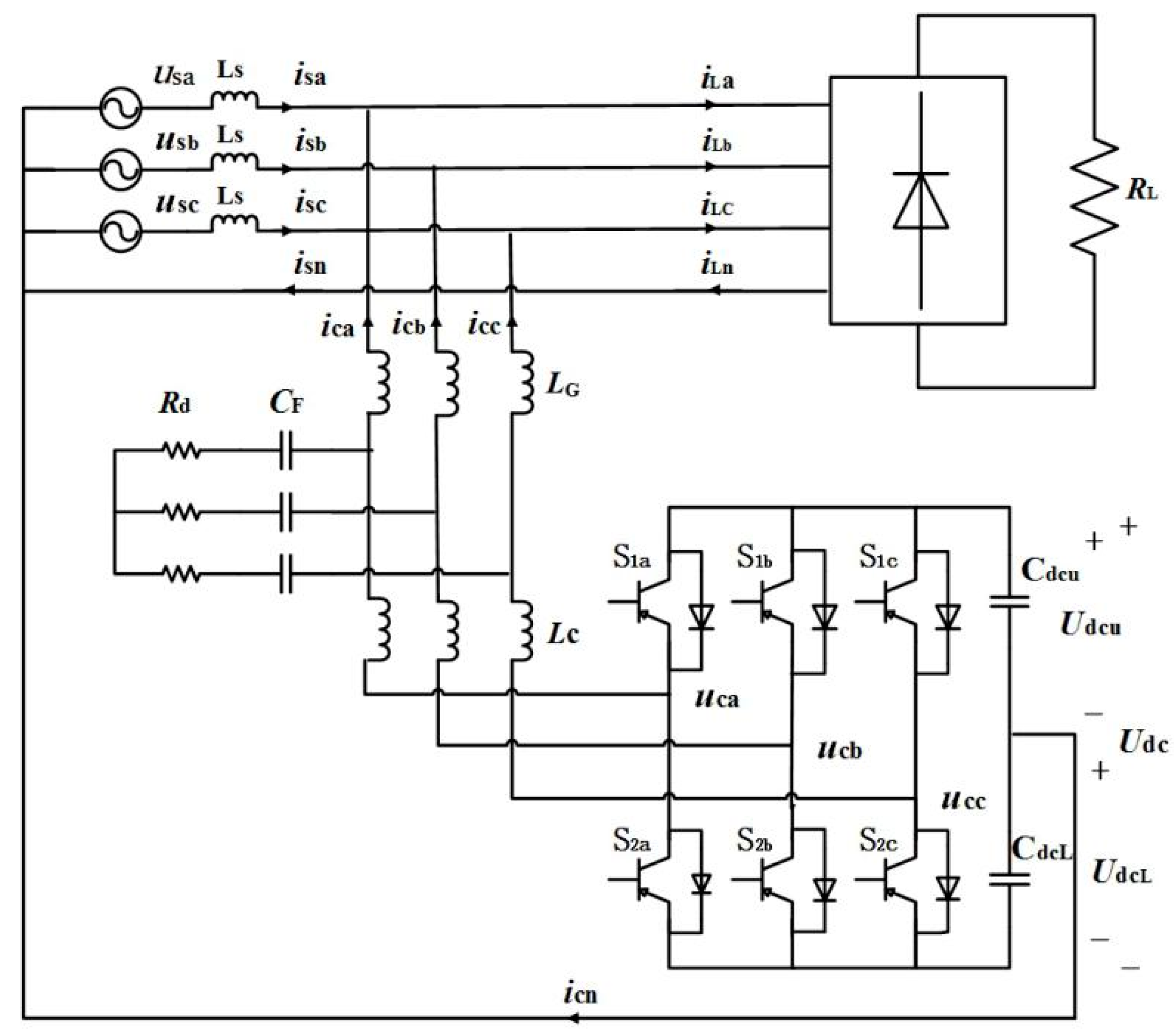
Figure 1 presents the topology of three-phase four-wire center-split shunt APF. From the figure,
usx is the grid voltage, and
ucx is the inverter output voltage. Besides,
isa,
isb and
isc are grid currents,
ica,
icb and
icc are compensating currents, and
iLa,
iLb and
iLc are load currents, and
Cdc is the DC-link capacitor.
Udc is the DC-link voltage, where
UdcU =
UdcL = 0.5
Udc.
R is the equivalent resistance of inductor. A resistance
RL and a three-phase full bridge rectifier constitute the non-linear load. The LCL filter is consisted of
LC,
LG,
CF, and the LCL filter is simplified to be an inductor with the value
L =
LC +
LG.
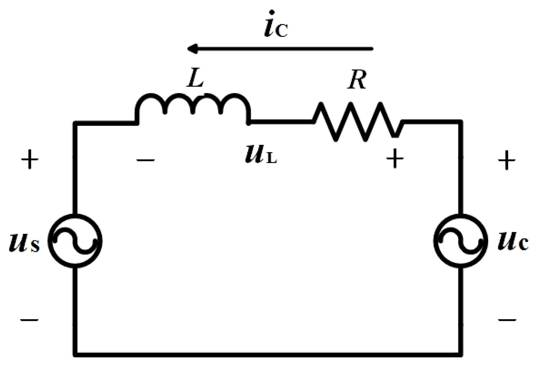
From
Figure 1, the single-phase equivalent circuit for each phase is presented in
Figure 2. From the figure, the inverter output voltage is:
From Equation (1), the inverter voltage in APF can be calculated by grid voltage, equivalent inductance, equivalent resistance, and compensating current.
Generally, the non-linear load currents
iL contains the fundamental current
iL1 and harmonic currents
iLh:
where
IL1x and
ILhx are the effective values of
iL1 and
iLhx.
Actually, APF compensating current
ic contains the fundamental component
ic1, the harmonic component
ich and also the switching frequency harmonic current
icsw:
In Equation (3), the fundamental current ic1, which compensates system power loss and maintains the DC-link voltage, is very small during a steady-state situation, and it is neglected during a steady-state operation.
Additionally, to compensate the load harmonics, the compensation component in compensating current is equaled to the harmonic components in load current presented in Equation (2). Thus, the compensating current
ich is:
Moreover, since the APF usually uses pulse width modulation (PWM) technology to generate the compensating currents, the compensating currents not only contain the required compensation component, but also contain the switching frequency harmonic current
icsw. Generally, the
icsw can be attenuated by applying the composite current tracking method, the space vector pulse width modulation (SVPWM), and optimized designed LCL filter. However, the above methods cannot guarantee eliminating the switching frequency harmonic current completely under varied working conditions, and their implementation processes are also complicated. Therefore, the switching frequency harmonic current
icsw should be considered during the compensating current analysis, and the switching frequency harmonic current
icsw can be described as:
where
Icsw is the effective value of switching frequency harmonic current, and
b =
fsw/
f.
Substituting Equations (4) and (5) into Equation (3), the APF compensating current
ic can be described as:
Then, in a three-phase symmetrical power system, the grid voltages are:
where
Usn is the effective value of
usa,
usb and
usc, and
w is the fundamental angular frequency.
Substituting Equations (4) and (7) into Equation (1), the inverter voltages can be described as:
Therefore, the inverter voltage can also be expressed as:
where
uc1 is the fundamental component of
uc,
uch is used to produce compensating currents compensating load harmonics, and
ucsw is the inverter voltage at switching frequency.
Then, the mold length of inverter voltage vector is:
From Equations (7)–(10), the maximal value of inverter voltage mold is:
To provide the sufficient DC-link voltage to generate compensating currents, the following equation needs to be satisfied:
where
m is modulation index.
To compensate harmonic currents, the APF needs to produce a voltage exceed the maximal value of inverter voltage vector mold. From Equation (12), the minimum DC-link voltage can be obtained:
During the steady-state operation, the DC-link voltage maintains at minimum value, and APF generates compensating currents to compensate the load harmonics. When the DC-link voltage becomes larger than the minimum value, the effective value of inverter output voltage increases. From Equations (11)–(13), the DC-link voltage determines the ability of producing compensating currents, and following equations can be obtained:
Generally, the effective value of harmonic currents
Ich are determined by harmonic detection algorithm calculated from the load currents, and they remain stable during steady-state operation. From Equation (14), the switching frequency harmonic current
Isw can be described as:
According to Equation (15), with the stable effective value of grid voltage Usn, equivalent inductance L, equivalent resistance R and compensating harmonic currents Ich calculated from load currents, the increase of DC-link voltage Udc may lead to the increase in effective value of switching frequency harmonic current Icsw.
Generally, the total harmonic distortion (THD) is an important indicator of compensation performance, and it can be expressed as:
As can be seen from Equation (16), the THD is not only affected by the nth harmonic currents In, but also affected by the switching frequency harmonic current Isw.
Therefore, according to Equations (15) and (16), the increase of DC-link voltage Udc leads to the increase of switching frequency harmonic current Icsw, thereby raising the THD value and deteriorate the compensation performance. Therefore, to prevent the increase of the DC-link voltage from deteriorating the compensation performance, the DC-link voltage should be maintained at the minimum value.
3. Proposed Simplified Minimum DC-Link Voltage Control Strategy
Substituting Equations (7) and (8) into Equation (1), the inverter voltage can be described as:
Make the transformation of the inverter voltages from the stationary abc coordinate system to the stationary α-β coordinate system with coordinate transformation formula T
abc-αβ:
Substituting Equation (17) into Equation (18), the inverter voltages in the stationary α-β coordinate are:
In Equation (19), since the values of harmonic components and their arithmetic combinations are small compared with effective value of grid voltage
Usn, they can be ignored to simplify the calculation. Therefore, the mold length of the inverter output voltage vector is:
To produce compensating currents to eliminate the load harmonics, the APF inverter voltage exceeds the maximal value of inverter voltage vector. Substituting Equation (20) into Equation (13), the following equation is obtained:
where
Umar is the voltage margin with a small value to control the switching frequency harmonic current and other factors.
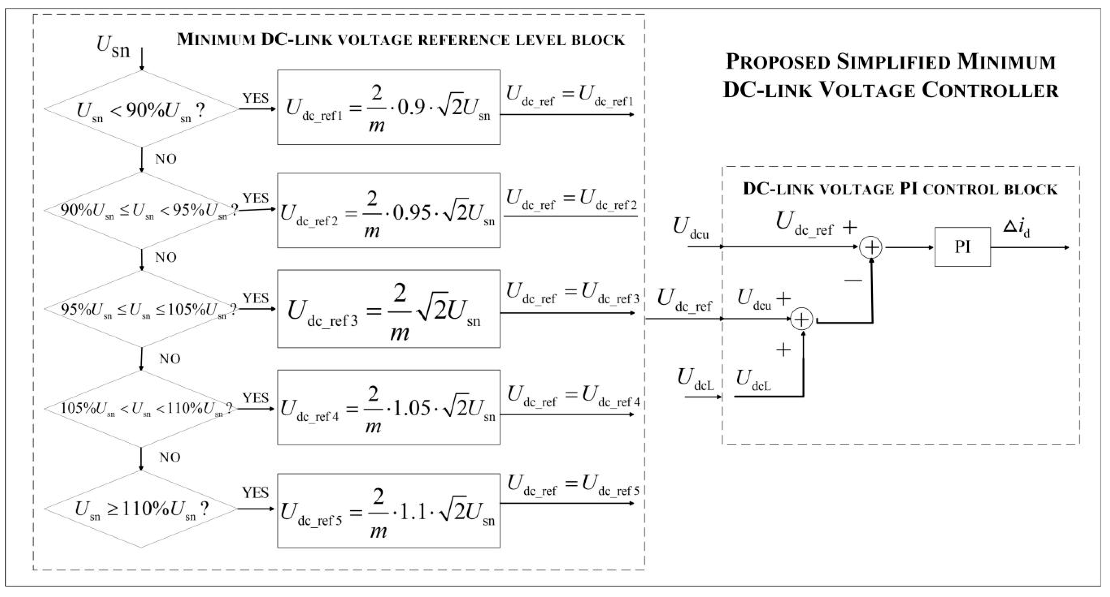
The control diagram of the proposed strategy is presented in
Figure 3. From the figure, the DC-link voltage reference value is initially set to be a minimum value calculated by the grid voltage and modulation index according to Equation (21), reducing the power consumption and switching loss. Additionally, the grid voltage may vary occasionally in practical application, leading to the frequent change of DC-link voltage reference value. To solve this issue, the DC-link voltage value under the proposed strategy is classified into certain levels according to different ranges of the grid voltage for selection. Thus, the reference DC-link voltage maintains at a constant value within a specific range. Furthermore, the DC-link voltage reference value under proposed strategy varies adaptively with the change of grid voltage, maintaining DC-link voltage at the minimum value in varied operating conditions.
Compared with the existing minimum DC-link voltage control strategy, the proposed minimum DC-link voltage is only determined by the grid voltage and modulation index, avoiding the influence from variations of equivalent parameters, reactive power and harmonic currents, thus improving the stability, reliability, and real-time characteristic of APF. Additionally, the proposed DC-link voltage minimum value avoids complex calculation of equivalent parameters, harmonic currents, and reactive power, reducing the calculation burden of processor. The comparison of calculation burden between the conventional and the proposed minimum DC-link voltage control strategy is listed in
Table 1. The minimum DC-link voltage calculation in [
27] contains four additions and subtractions and 16 multiplications and divisions, and the calculation in [
28] contains 20 additions and subtractions and eight multiplications and divisions. This brings a large calculation burden to the processor. By applying the proposed strategy, the addition and subtraction calculations are not needed, and the number of the multiplication and division reduces to three, thus reducing the calculation burden on processor and improving the real-time characteristics for APF.
4. Experiment Verification
Figure 4 presents a shunt APF prototype established in laboratory, and the parameters are shown in
Table 2. Without APF, the grid current contains a large number of harmonics, and the THD of the experimental grid current is 23.63%. Based on the deduction, the APF minimum DC-link voltage under the proposed simplified strategy can be calculated from Equation (21). Thus, with the grid voltage
Usn = 220 V, the minimum DC-link voltage
Udc-ref = 630 V. When the
Udc = 620 V, lower than minimum value 630 V, the experimental results are shown in
Figure 5. From the figure, the grid current after compensation still contains a large number of harmonics, and it is not an ideal sine waveform. Furthermore, the grid current THD after compensation is 11.05%, and it does not ideally compensate performance. The results illustrate that, when
Udc is lower than the minimum value, APF cannot largely compensate the harmonics and achieve an ideal compensation performance.
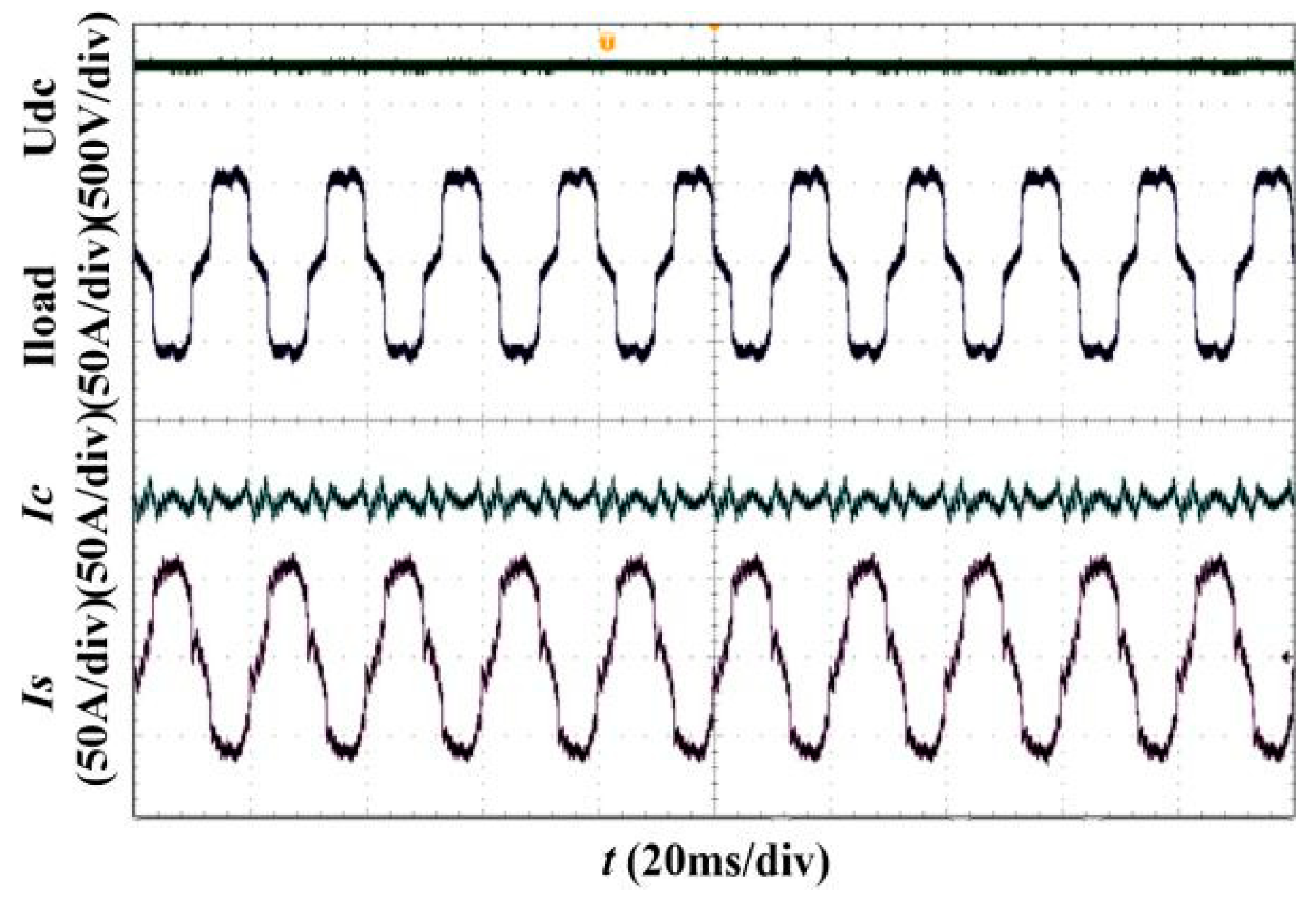
Then, when
Udc = 640 V, higher than the minimum value 630 V, the experimental results are shown in
Figure 6a. The load harmonics are greatly compensated, and the grid currents are nearly sinusoidal waveforms. Additionally, the grid current distortions are almost eliminated, and the grid current THD after compensation is 5.65%, thus satisfying the international standards. In addition, the experimental voltages and currents with
Udc = 660 V are shown in
Figure 6b. Compared with the voltages and currents with
Udc = 640 V and
Udc = 660 V, the grid currents after compensation are both nearly sinusoidal waveforms, and harmonic components are largely compensated. Therefore, when the DC-link voltage becomes higher than the minimum value, the APF achieves an ideal compensation performance.
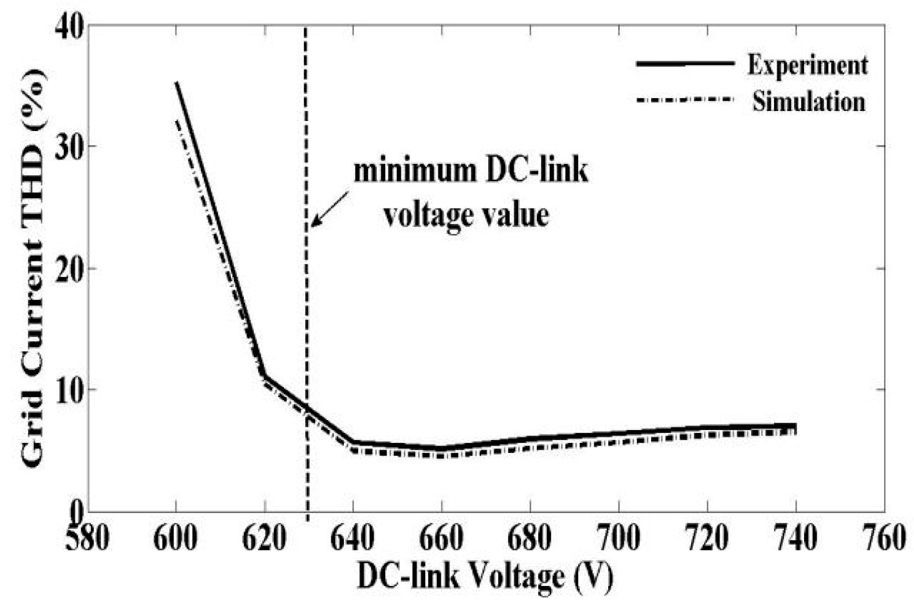
With the increase of DC-link voltage value, the THD values of simulation and experiment grid current after compensation with the different
Udc are presented in
Table 3, and the THDs with different DC-link voltages are presented in
Figure 7. The results illustrate that, when the DC-link voltage becomes lower than the minimum value, APF cannot compensate harmonics completely, and the compensation performance even deteriorates with the decrease of DC-link voltage. Additionally, when the DC-link voltage becomes larger than the minimum value, the increase of DC-link voltage cannot improve the APF compensation performance, but increases the THD of grid current and deteriorates the compensation effect.
Although the THDs of grid currents with varied DC-link voltages are different, it is difficult to recognize from the voltage and current waveforms. Thus, the values of compensating current in each order with varied DC-link voltages are presented in
Table 4. From the table, with the increase of the DC-link voltage, the values of each order in compensating currents vary slightly, due to the compensating currents strictly following the reference compensating currents obtained from the harmonic detection section. However, the switching frequency harmonic current increase obviously with the increase of the DC-link voltage. As mentioned above, the THD is calculated with every order in compensating the current, including the switching frequency harmonic current. Therefore, the increase of the DC-link voltage leads to the increase of the switching frequency harmonic current, leading to the increase of the THD value, but not the improvement of the compensation effect, and the influence becomes more serious with the further increase of the DC-link voltage. Therefore, when the DC-link voltage is higher than the minimum value, the increase of the DC-link voltage cannot improve, but brings the deterioration in the compensation effect. To avoid the deterioration in the compensation and achieve an ideal compensation performance, the DC-link voltage should be maintained at a minimum value.
Moreover, when the effective value of grid voltage varies form
Usn = 220 V to 198 V, the required minimum DC-link voltage value changes to
Udc-ref = 575 V accordingly. Under the proposed strategy, the DC-link voltage varies adaptively and maintains at a new minimum value, as shown in
Figure 8. Additionally, the dynamic behavior of currents during the transient is not obvious. This is because the transient is not caused by a variation of the load, but caused by a variation of the grid voltage, resulting in a variation of the DC-link voltage. In the APF, the dynamic in current control loop is much faster than that in voltage control loop, thus the disturbance from the voltage loop causes a very small current distortion during the transient. Thus, with the DC-link voltage obtained by the proposed strategy, the load harmonic currents are still significantly compensated and the grid current distortion is almost eliminated. After compensation, the THD of the grid current is 5.52%. The results verify that, under the proposed strategy, the DC-link voltage can vary adaptively to maintain the minimum value with the varied grid voltage situation and ensure the ideal APF compensation performance.
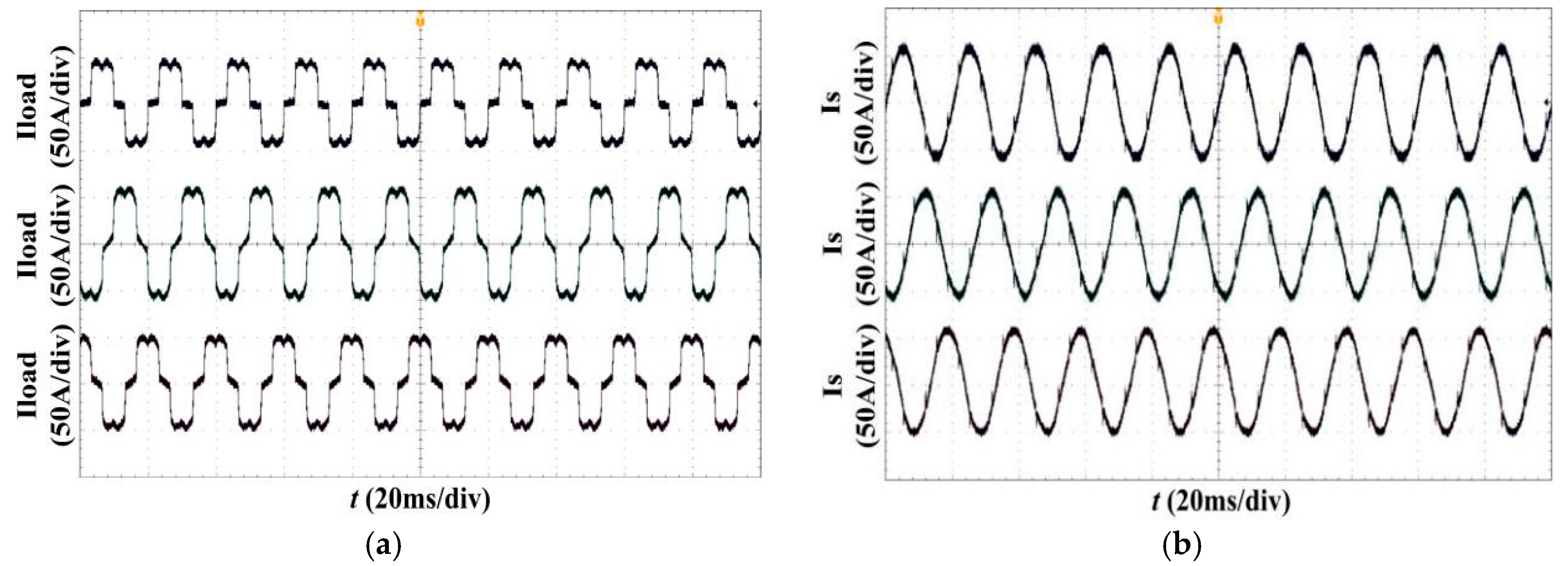
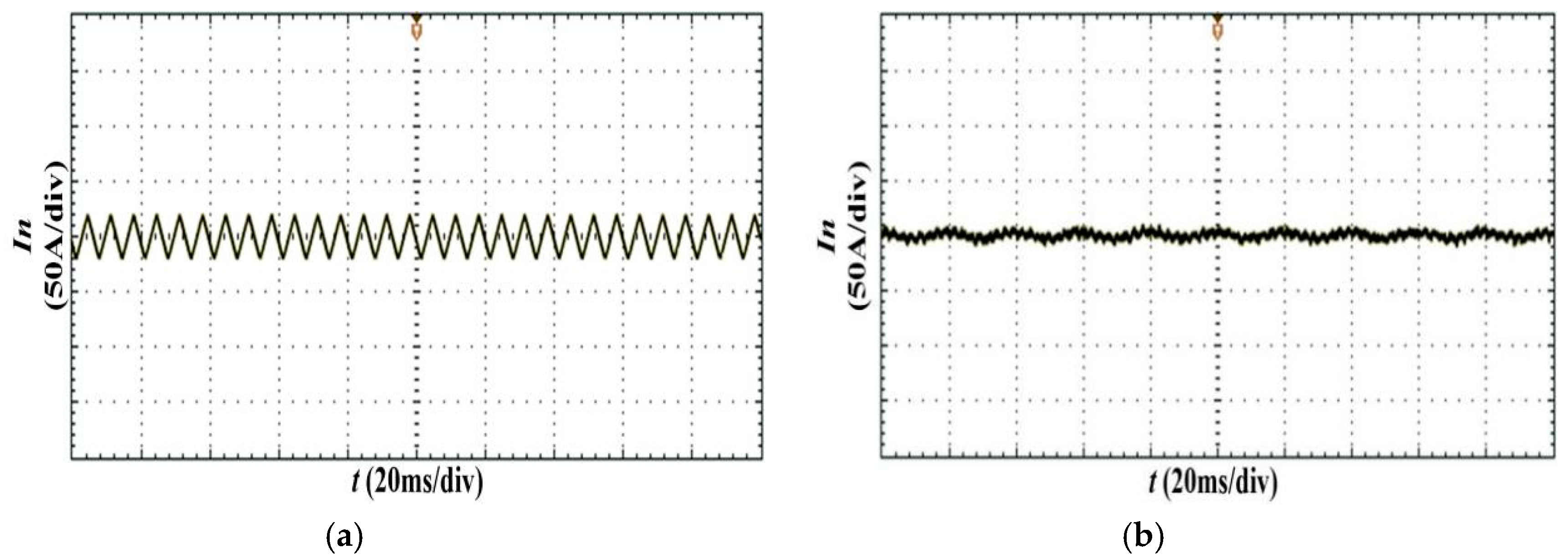
Furthermore, the experiment results in an unbalanced load are shown in
Figure 9. From the figures, the grid current in a, b, and c phases before compensation are 35.8 A, 45.3 A, and 37.8 A, respectively. When applying the proposed strategy in APF, the load harmonics are greatly compensated, and the grid currents are all sinusoidal waveforms and 45.2 A, 46.8 A, and 45.8 A in a, b, and c phase, respectively. Moreover, the neutral line current is
in = 11.2 A with the unbalance load, as shown in
Figure 10a. After compensation by the APF under the proposed the DC-link voltage strategy, the neutral current drops to about
in = 1.7 A, as shown in
Figure 10b. The experimental results show that the APF under proposed DC-link voltage strategy can also compensate the neutral current in unbalanced load application, reducing the influence from neutral current to the system, and the unbalanced load phenomenon is eliminated effectively. Therefore, the proposed strategy can be applied in the unbalanced load situation and also achieves an ideal APF compensation performance.


