A Power and Data Decoupled Transmission Method for Wireless Power Transfer Systems via a Shared Inductive Link


Abstract
1. Introduction
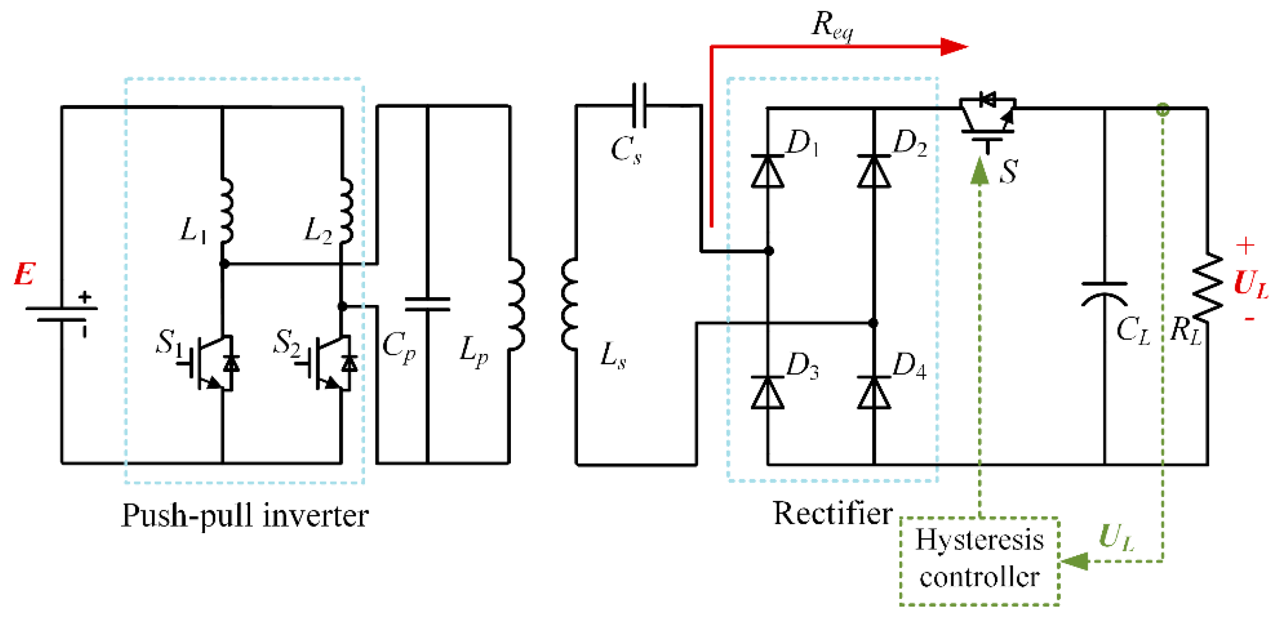
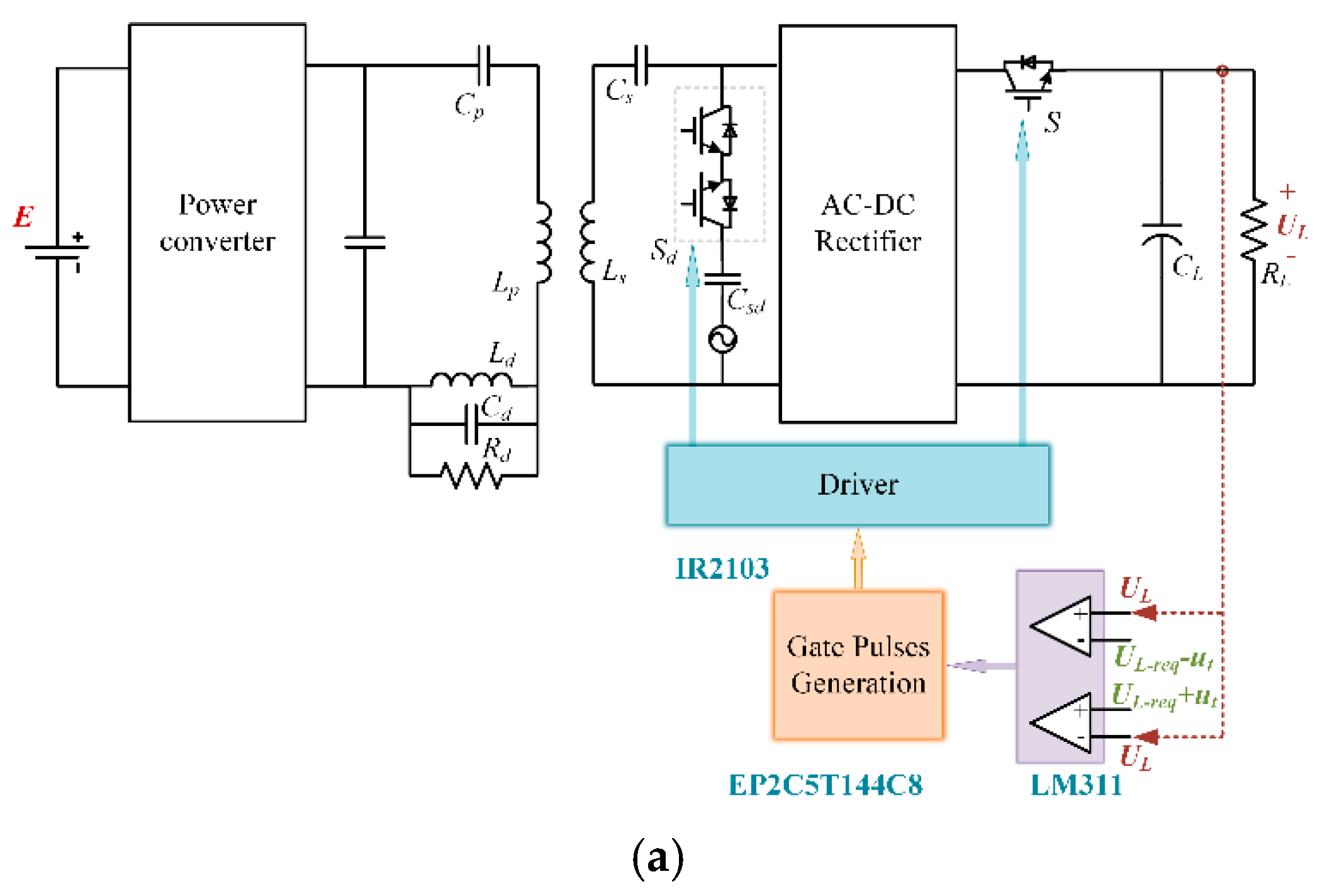
2. System Overview
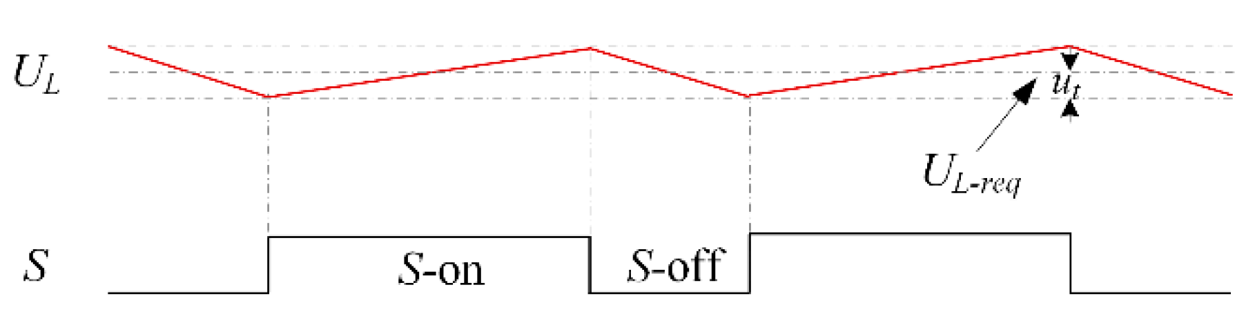
2.1. Hysteresis Voltage Control
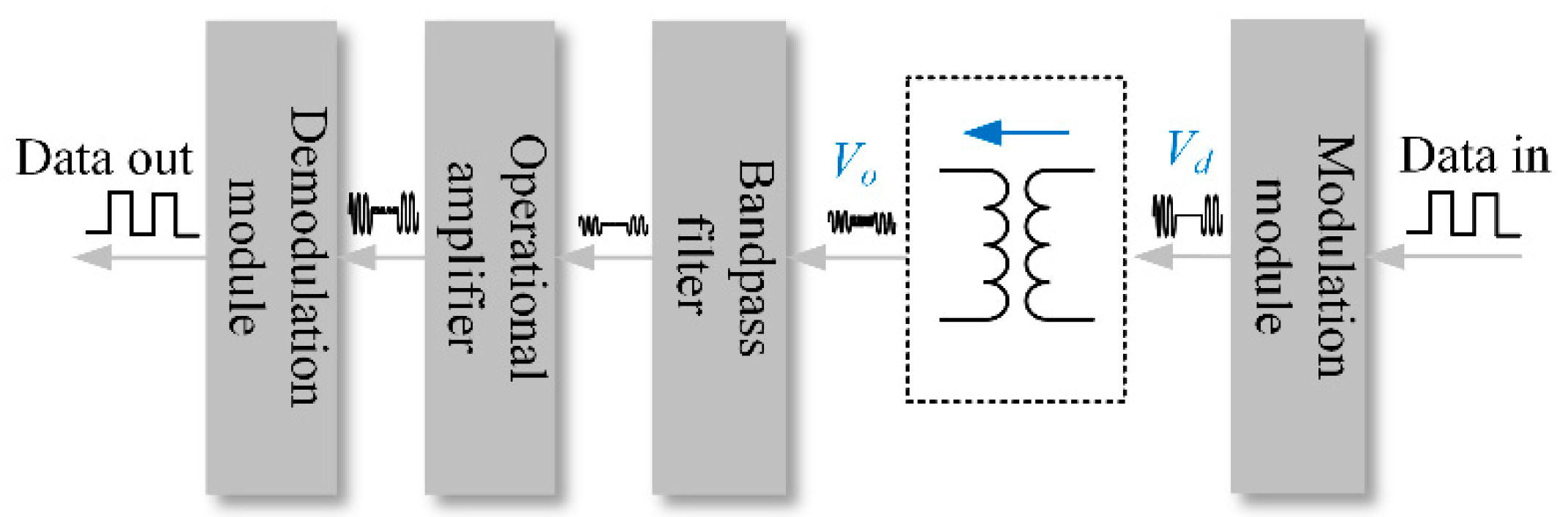
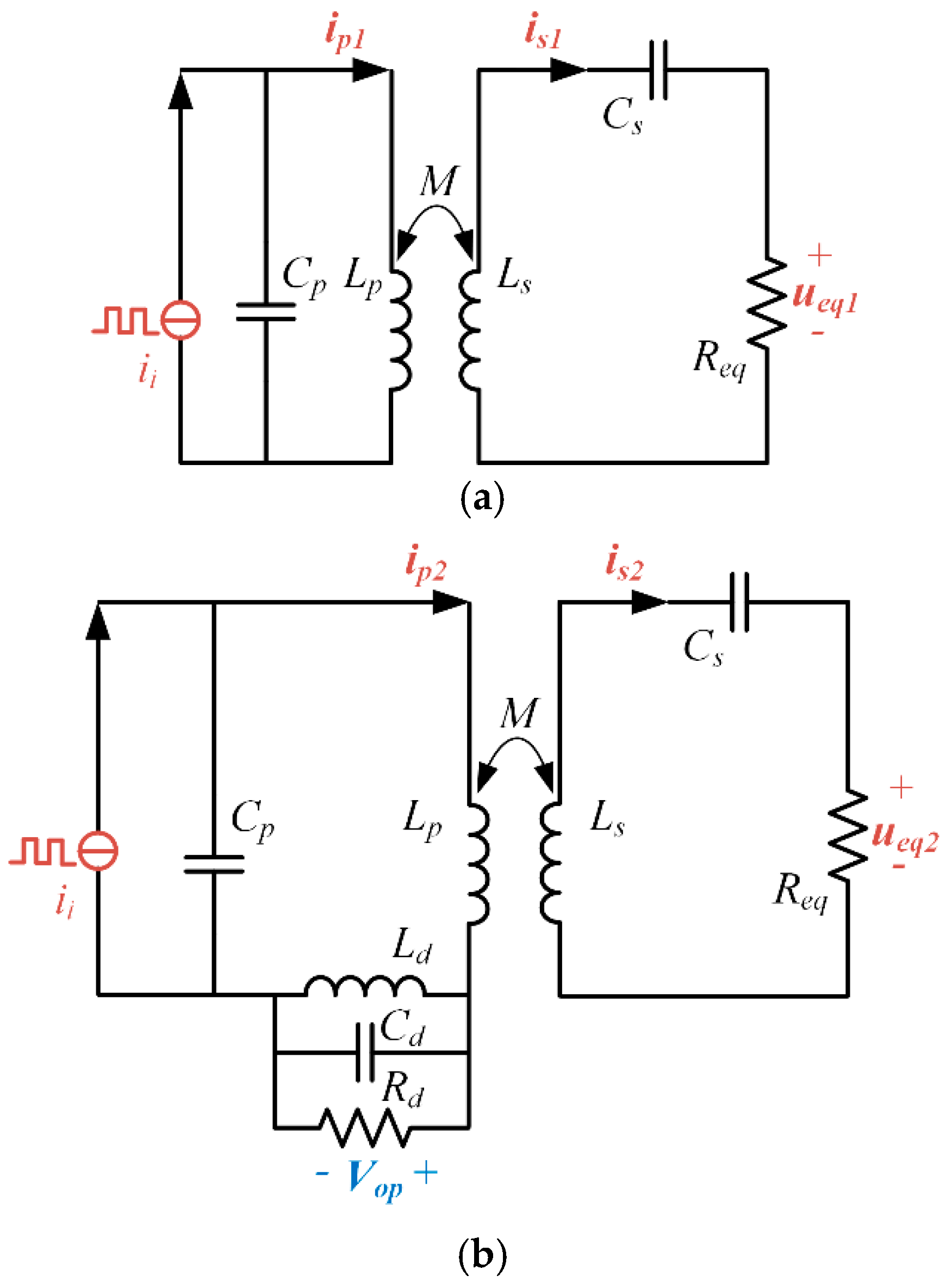
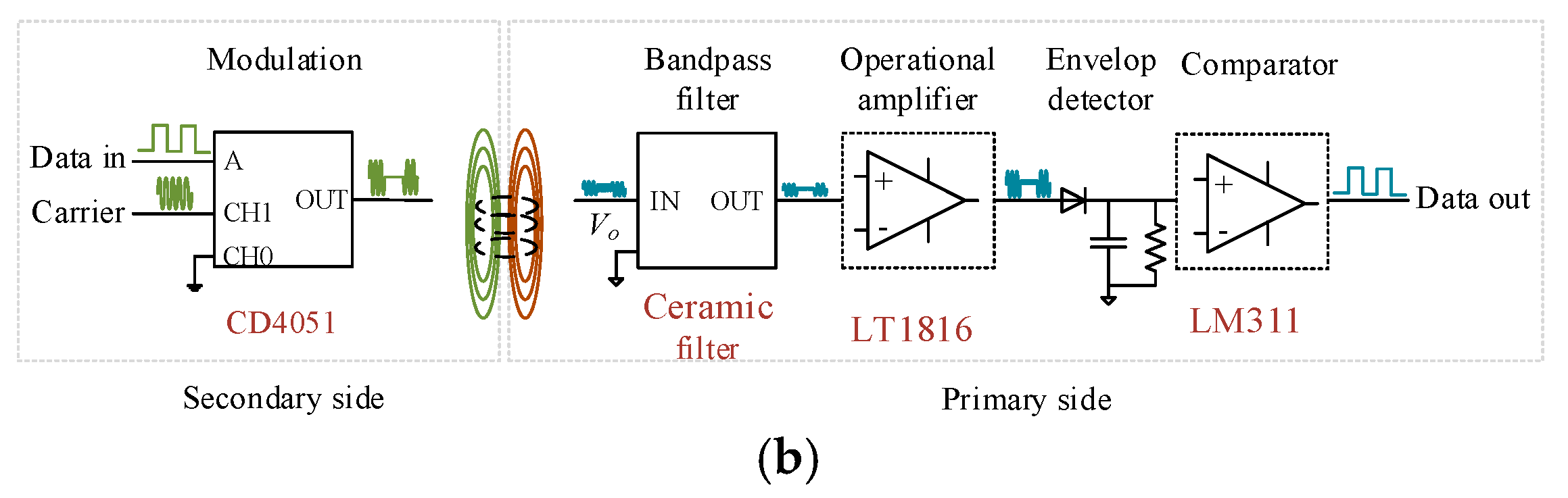
2.2. Power and Data Transfer Principle
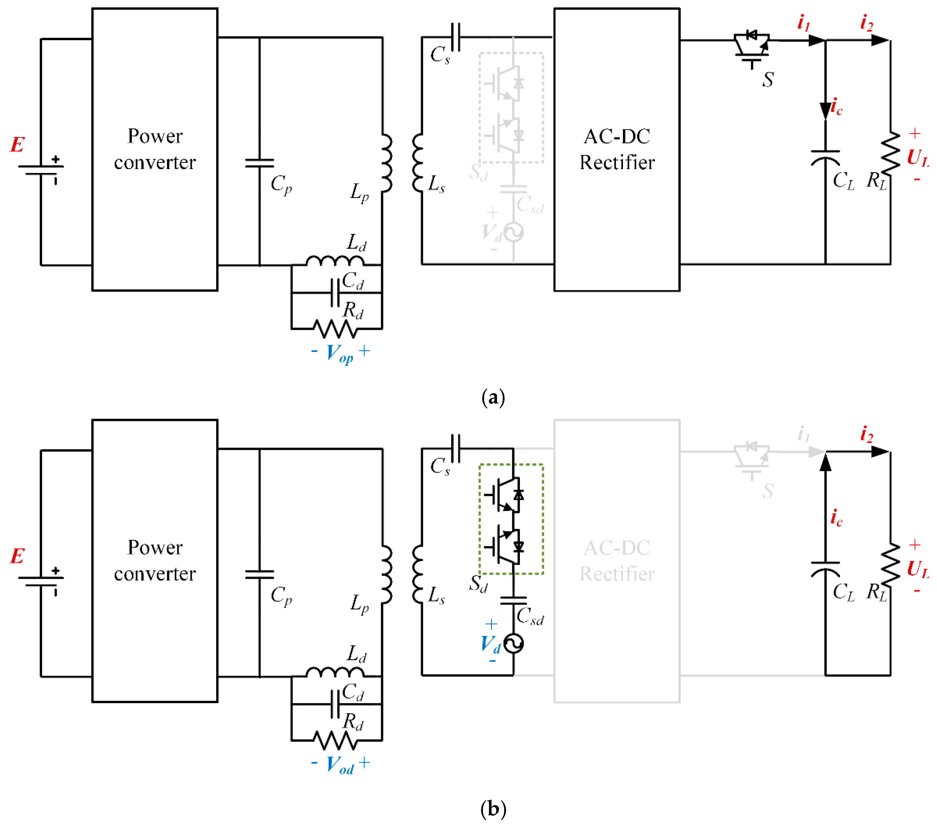
3. Interference of Extra Data Transfer Channel on Power Transfer
3.1. Interference of Extra Data Transfer Channel on Power Transfer
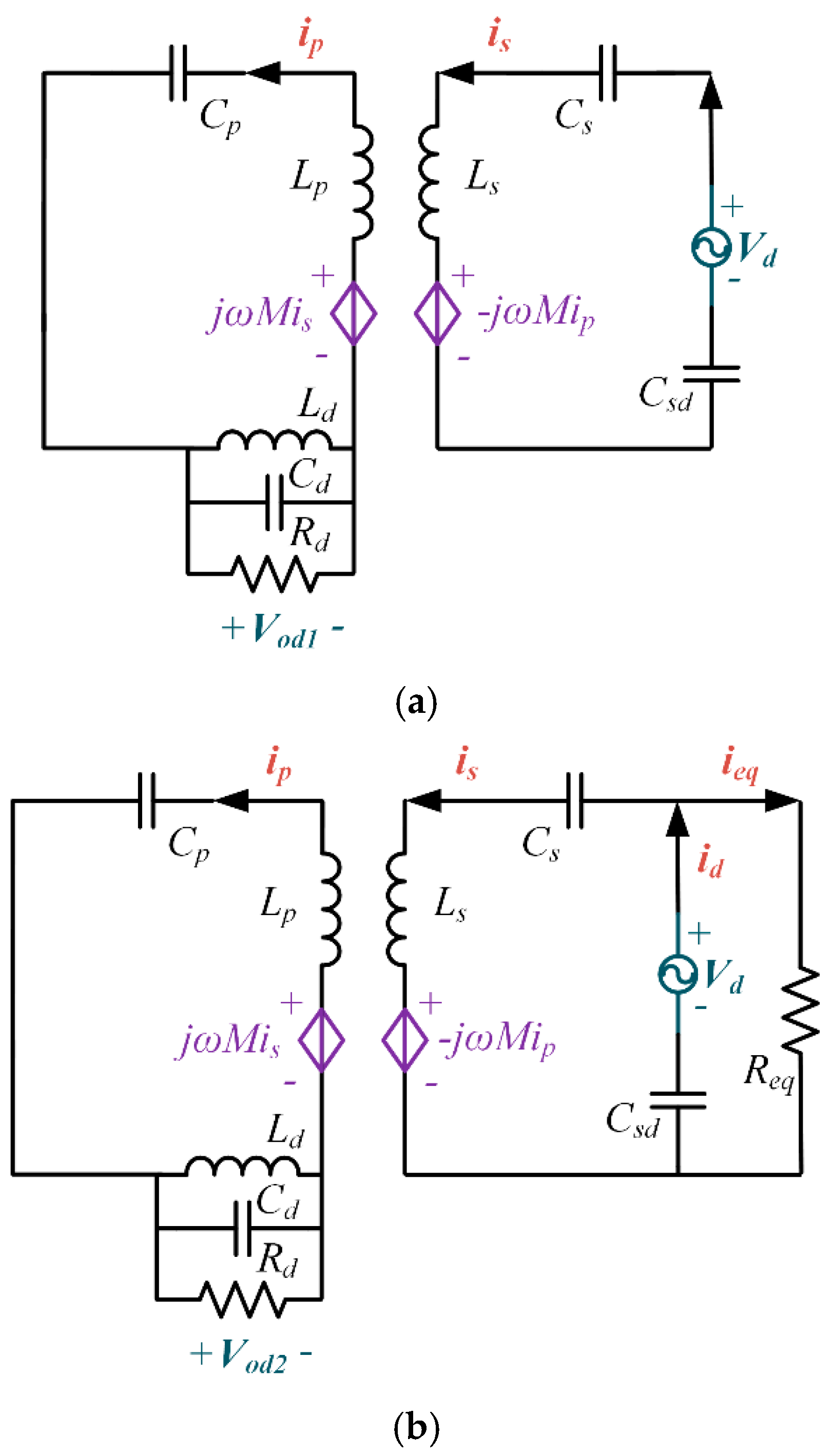
3.2. Interference of Power Transfer on Data Transfer
3.3. Data Transfer Channel Analysis
3.4. Consideration for the Data Transfer Rate
4. Simulation Studies
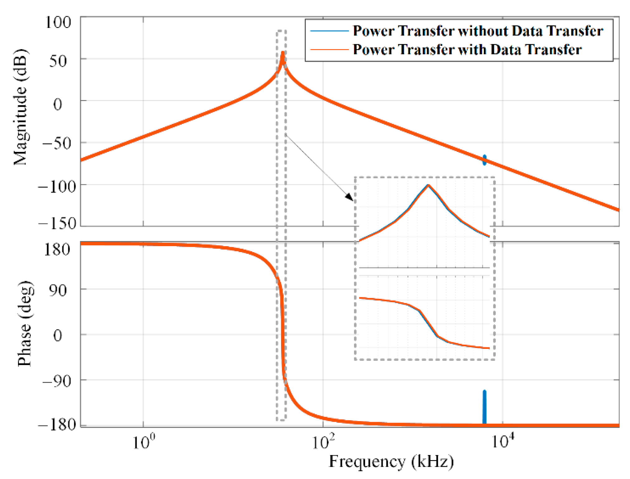
4.1. Bode Plot Analysis of Power Transfer with and without Data Transfer
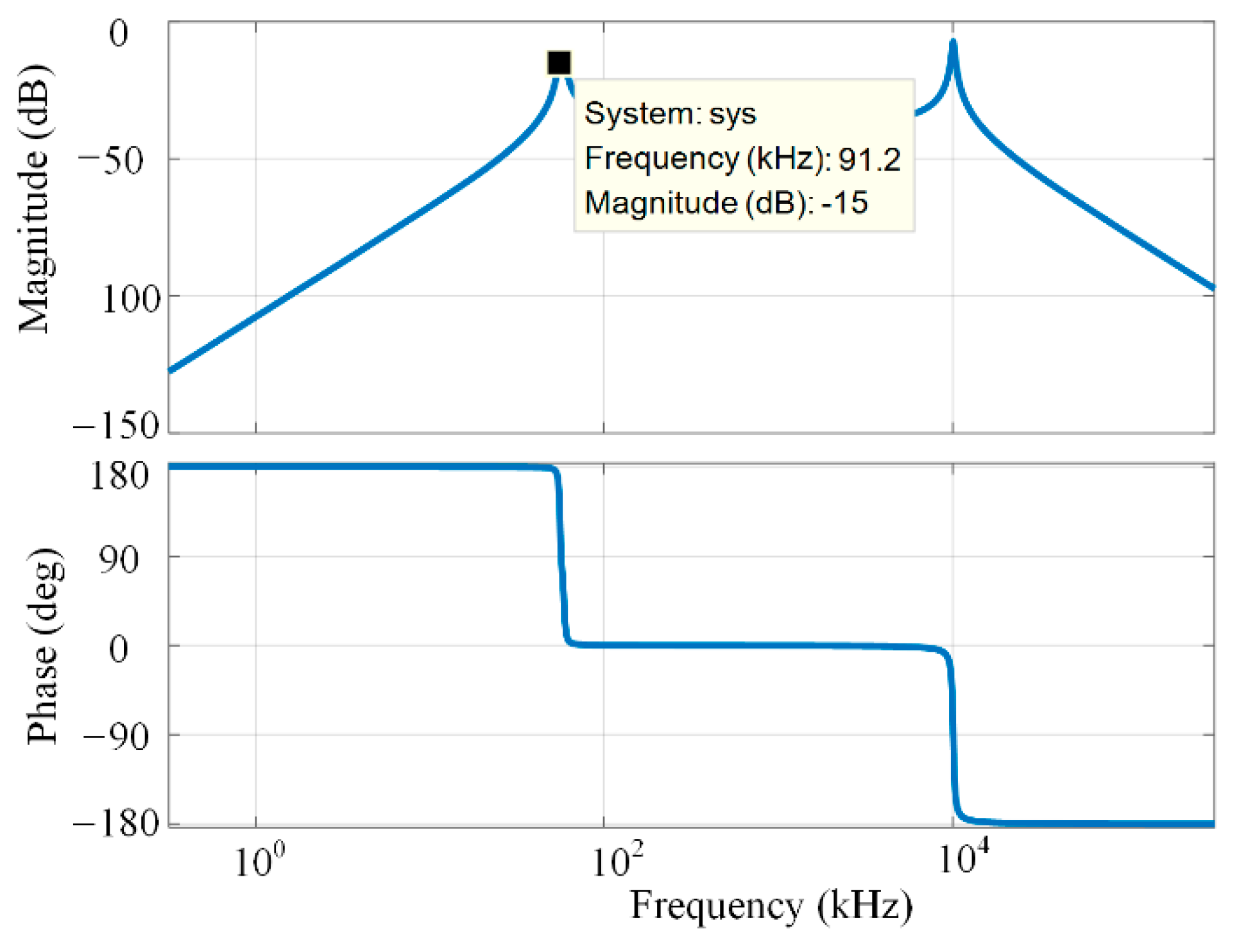
4.2. Bode Plot of the Interference from Power Transfer to Data Transfer
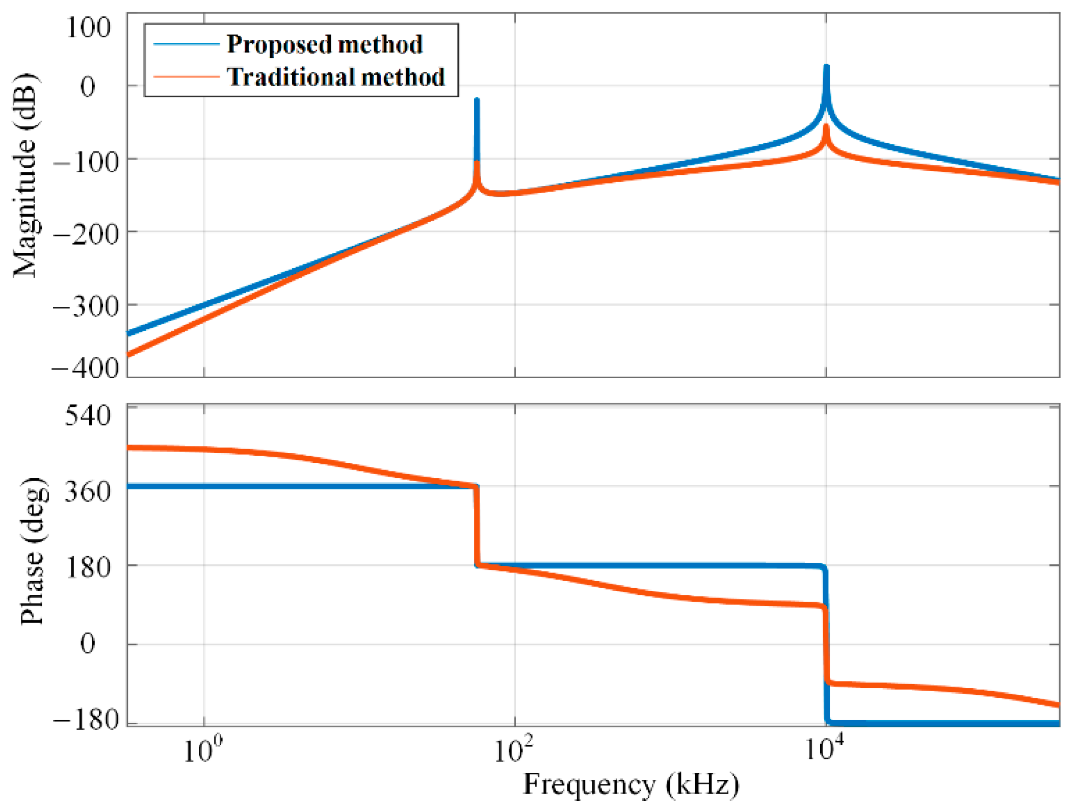
4.3. Bode Plot Analysis of the Proposed and Traditional Data Transfer Channel
5. Experimental Verification
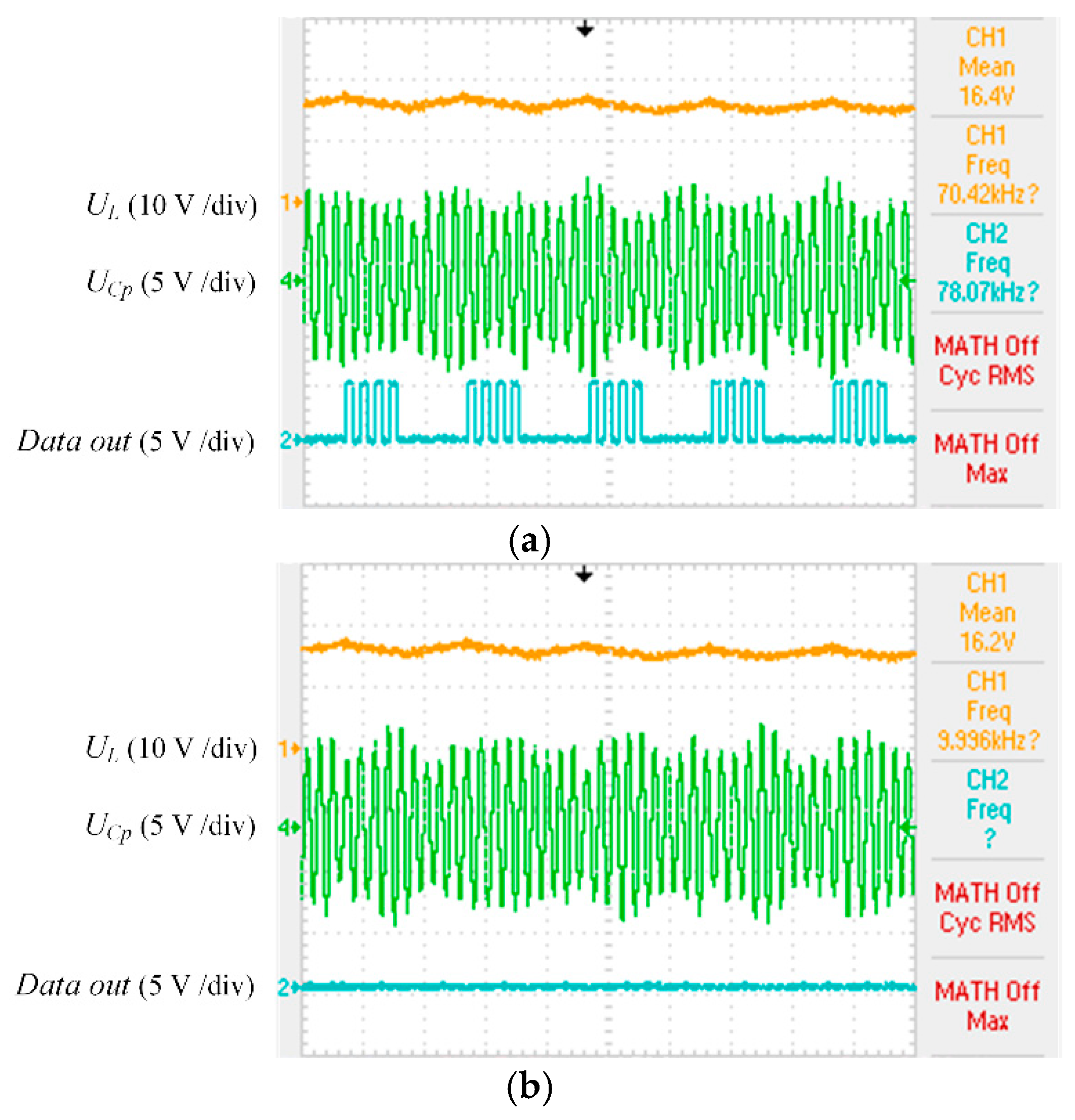
5.1. Interference Analysis of the Data Transfer Channel to Power Transfer
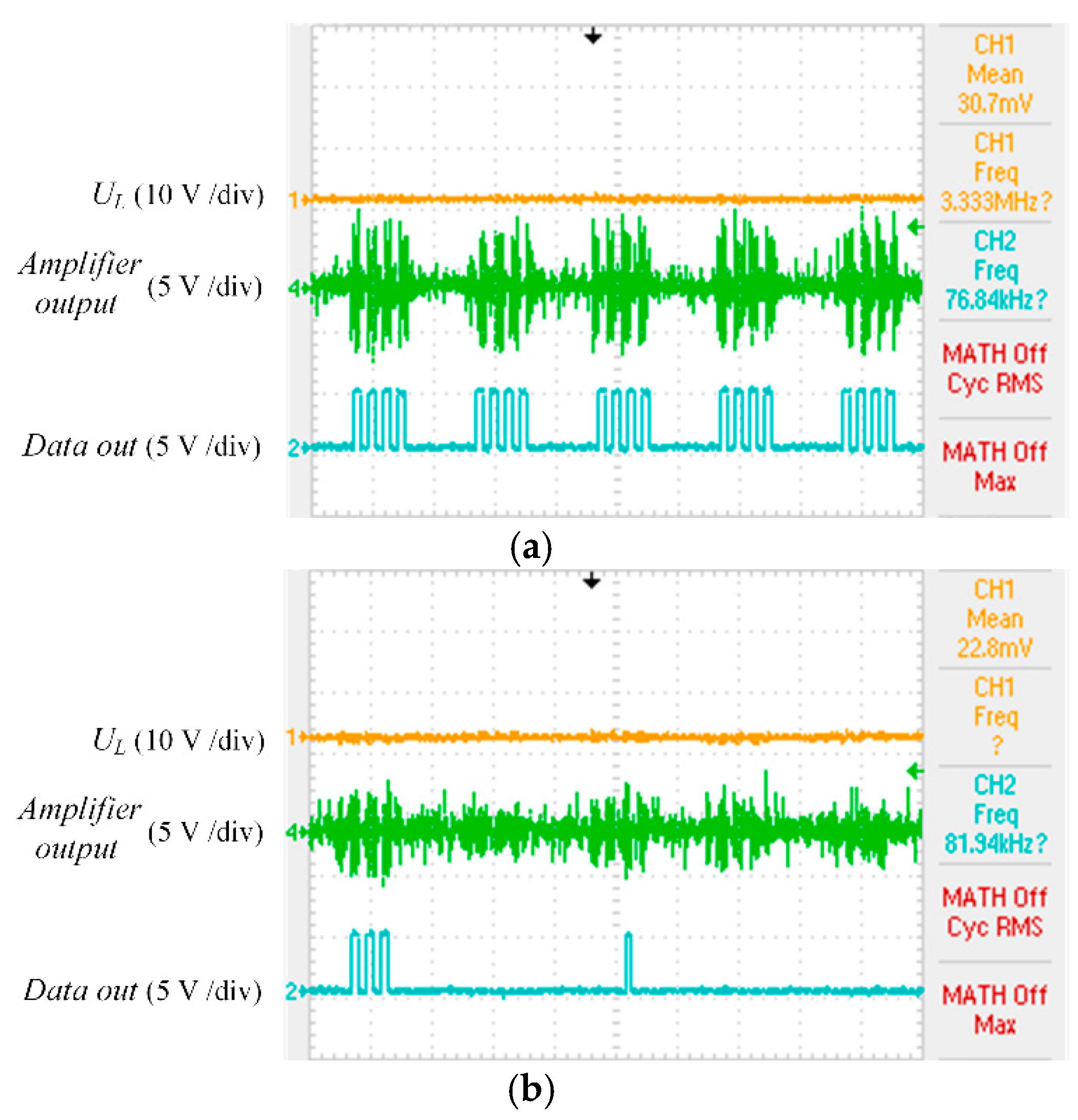
5.2. Comparison between the Proposed and Traditional Data Transfer Method
5.3. Analysis of the Data Transfer Rate
5.4. Comparasion Results with the Published Literatures
6. Conclusions
Author Contributions
Funding
Acknowledgments
Conflicts of Interest
References
- Covic, G.A.; Boys, J.T. Inductive Power Transfer. Proc. IEEE 2013, 101, 1276–1289. [Google Scholar] [CrossRef]
- Hui, S.Y.R. Planar Wireless Charging Technology for Portable Electronic Products and Qi. Proc. IEEE 2013, 101, 1290–1301. [Google Scholar] [CrossRef]
- Mi, C.; Buja, G.; Choi, S.Y.; Rim, C.T. Modern advances in wireless power transfer systems for roadway powered electric vehicles. IEEE Trans. Ind. Electron. 2016, 63, 6533–6545. [Google Scholar] [CrossRef]
- Hui, S.Y.R. Magnetic Resonance for Wireless Power Transfer [A Look Back]. IEEE Power Electron. Mag. 2016, 3, 14–31. [Google Scholar] [CrossRef]
- Dai, X.; Li, X.; Li, Y.; Hu, A.P. Maximum Efficiency Tracking for Wireless Power Transfer Systems with Dynamic Coupling Coefficient Estimation. IEEE Trans. Power. Electron. 2018, 33, 5005–5015. [Google Scholar] [CrossRef]
- Qu, X.; Han, H.; Wong, S.C.; Tse, C.K.; Chen, W. Hybrid IPT Topologies with Constant Current or Constant Voltage Output for Battery Charging Applications. IEEE Trans. Power. Electron. 2015, 30, 6329–6337. [Google Scholar] [CrossRef]
- Chen, L.; Boys, J.T.; Covic, G.A. Power Management for Multiple-Pickup IPT Systems in Materials Handling Applications. IEEE J. Emerg. Sel. Top. Power Electron. 2015, 3, 163–176. [Google Scholar] [CrossRef]
- Gati, E.; Kampitsis, G.; Manias, S. Variable Frequency Controller for Inductive Power Transfer in Dynamic Conditions. IEEE Trans. Power. Electron. 2017, 32, 1684–1696. [Google Scholar] [CrossRef]
- Low, Z.N.; Chinga, R.A.; Tseng, R.; Lin, J. Design and test of a high-power high-efficiency loosely coupled planar wireless power transfer system. IEEE Trans. Ind. Electron. 2009, 56, 1801–1812. [Google Scholar]
- Li, H.; Li, J.; Wang, K.; Chen, W.; Yang, X. A Maximum Efficiency Point Tracking Control Scheme for Wireless Power Transfer Systems Using Magnetic Resonant Coupling. IEEE Trans. Power Electron. 2015, 30, 3998–4008. [Google Scholar] [CrossRef]
- Zhong, W.X.; Hui, S.Y.R. Maximum Energy Efficiency Tracking for Wireless Power Transfer Systems. IEEE Trans. Power Electron. 2015, 30, 4025–4034. [Google Scholar] [CrossRef]
- Zhong, W.X.; Hui, S.Y.R. Maximum Energy Efficiency Operation of Series-Series Resonant Wireless Power Transfer Systems Using On-Off Keying Modulation. IEEE Trans. Power. Electron. 2018, 33, 3595–3603. [Google Scholar] [CrossRef]
- Huang, C.C.; Lin, C.L.; Wu, Y.K. Simultaneous wireless power/data transfer for electric vehicle charging. IEEE Trans. Ind. Electron. 2017, 64, 682–690. [Google Scholar] [CrossRef]
- Li, X.; Tang, C.; Dai, X.; Deng, P.; Su, Y. An Inductive and Capacitive Combined Parallel Transmission of Power and Data for Wireless Power Transfer Systems. IEEE Trans. Power. Electron. 2018, 33, 4980–4991. [Google Scholar] [CrossRef]
- Wu, J.; Zhao, C.; Lin, Z.; Du, J.; Hu, Y.; He, X. Wireless power and data transfer via a common inductive link using frequency division multiplexing. IEEE Trans. Ind. Electron. 2015, 62, 7810–7820. [Google Scholar] [CrossRef]
- Sun, Y.; Yan, P.X.; Wang, Z.H.; Luan, Y.Y. The parallel transmission of power and data with the shared channel for an inductive power transfer system. IEEE Trans. Power Electron. 2016, 31, 5495–5502. [Google Scholar] [CrossRef]
- Wang, G.; Wang, P.; Tang, Y. Analysis of dual band power and data telemetry for biomedical implants. IEEE Trans. Biomed. Circuits Syst. 2012, 6, 208–215. [Google Scholar] [CrossRef] [PubMed]
- Zhou, Y.; Zhu, X.; Wu, L.; Wang, B. Study of Wireless Power and Information Transmission Technology based on the Triangular Current Waveform. IEEE Trans. Power. Electron. 2018, 33, 1368–1377. [Google Scholar]
- Wu, J.; Zong, S.; He, X. Power/signal time division multiplexing technique based on power electronic circuits. In Proceedings of the 26th Annual IEEE Applied Power Electronics Conference and Exposition (APEC), Fort Worth, TX, USA, 6–10 March 2011; pp. 1710–1714. [Google Scholar]
- Jiang, C.; Chau, K.T.; Ching, T.W.; Liu, C.; Han, W. Time-Division Multiplexing Wireless Power Transfer for Separately Excited DC Motor Drives. IEEE Trans. Mag. 2017, 53, 1–5. [Google Scholar] [CrossRef]


| Parameter | Value | Parameter | Value |
|---|---|---|---|
| Lp | 50 μH | Ls | 50 μH |
| Cp | 60 nF | Cs | 61 nF |
| M | 12.9 μH | E | 20 V |
| L1,L2 | 150 μH | RL | 10 Ω |
| fp UL-req | 91 kHz 16 V | fd ut | 10 MHz 0.5 V |
| Reference | Bit Rate (kbps) | Transferred Power(W) | Potential Applications |
|---|---|---|---|
| [13] | 2.16 | 700 | EVs (Electrical Vehicles) |
| [14] | 230 | 40 | Peer to peer wireless power transfer (WPT)) with metal shielding such as in EVs |
| [15] | 20 | 500 | High power WPT with low frequency such as in EVs |
| [16] | 19.2 | 250 | Drilling systems |
| [17] | N/A | N/A | Biomedical implants |
| [18] | 6 | N/A | N/A |
| This paper | 560 | 25 | Robots, biomedical implants, etc. |
© 2018 by the authors. Licensee MDPI, Basel, Switzerland. This article is an open access article distributed under the terms and conditions of the Creative Commons Attribution (CC BY) license (http://creativecommons.org/licenses/by/4.0/).
Share and Cite
Li, X.; Wang, H.; Dai, X. A Power and Data Decoupled Transmission Method for Wireless Power Transfer Systems via a Shared Inductive Link. Energies 2018, 11, 2161. https://doi.org/10.3390/en11082161
Li X, Wang H, Dai X. A Power and Data Decoupled Transmission Method for Wireless Power Transfer Systems via a Shared Inductive Link. Energies. 2018; 11(8):2161. https://doi.org/10.3390/en11082161
Chicago/Turabian StyleLi, Xiaofei, Haichao Wang, and Xin Dai. 2018. "A Power and Data Decoupled Transmission Method for Wireless Power Transfer Systems via a Shared Inductive Link" Energies 11, no. 8: 2161. https://doi.org/10.3390/en11082161
APA StyleLi, X., Wang, H., & Dai, X. (2018). A Power and Data Decoupled Transmission Method for Wireless Power Transfer Systems via a Shared Inductive Link. Energies, 11(8), 2161. https://doi.org/10.3390/en11082161