Article

A New Exact Mathematical Approach for Studying Bifurcation in DCM Operated dc-dc Switching Converters

Applied Electronics Department, Politehnica University Timişoara, Timișoara 300006, Romania
*
Author to whom correspondence should be addressed.
Energies 2018, 11(3), 663; https://doi.org/10.3390/en11030663
Submission received: 31 January 2018 / Revised: 27 February 2018 / Accepted: 13 March 2018 / Published: 15 March 2018

Abstract

:
A bifurcation study for dc-dc converters operated in DCM is performed using an accurate method. When applying classical techniques significant difficulties are encountered in the calculations. For example, using the averaging method the validity of the result is limited to half the switching frequency and higher order effects are neglected Another approach is to perform a Taylor expansion of the state transition matrices. However, this is somehow also an averaging but the fact that the Taylor series is truncated leads to unacceptable inaccuracy. A new mathematical technique for discontinuous conduction mode (DCM) analysis of dc-dc switching converters is proposed in order to predict bifurcation and chaos. The proposed technique is based on exact calculation of the state transition matrices and of the Jacobian thus providing higher accuracy of the results compared to other previously reported approaches. Beside the fact the new technique allows for exact diagnosis of instability, it is also highly general, in the sense that it can be applied to any dc-dc DCM operated converter employing any type of control. The good agreement between theoretical, simulation and experimental results, with an error lower than 0.94%, confirms the validity of the proposed method.

1. Introduction

Power electronic switching converters are highly nonlinear systems that give arise of various phenomena when a feedback loop is closed for control. In the past years much attention was dedicated to chaos and bifurcations analysis of switching converters with emphasis on dc-dc switching topologies employing different control strategies [1,2].
As known, dc-dc switching converters are mainly used in two operating modes: continuous conduction mode (CCM) and discontinuous conduction mode (DCM). In CCM the diode currents in the off state never reach zero and this mode occurs when the inductors are relatively high, while the load current and the switching frequency are also significant. At light loads, that is at low output currents or, equivalently, at higher load resistances, small inductor values or low switching frequencies the inductor current ripple becomes comparable to its dc value and the diode current, equal to a linear combination of inductor currents, is zero for a certain time interval during transistor off time.
In [3], a current-mode controlled boost converter was subjected to study, while a sampled-data modelling and analysis of PWM dc-dc converters in both CCM and DCM is carried out in [4]. A unified analysis of CCM converters employing different control techniques (e.g., one cycle control, charge control, etc.) is performed in [5,6,7,8] from a bifurcation point of view. The asynchronous switching map on studying the stability effects of circuit parameters in CCM fixed off-time controlled buck converter is performed in [9]. Bifurcations due to on-load parameter fluctuations that can occur at the boundary between CCM and DCM and discontinuity mapping were investigated for a boost converter in [10], developing the theory of border collision bifurcations for this special case.
From a chaotic point of view, in [11] a DCM voltage-controlled buck converter was presented. Some important studies regarding bifurcations in DCM were reported in [12,13]. A DCM buck converter with proportional control is provided in [14]. In [15] a current-mode pulse train (CMPT) control technique is used with a DCM operated converter, the effects of circuit parameters on the converter dynamics are analyzed and the border collision mechanism is revealed. The first bifurcation study reported on a DCM Ćuk converter employing current mode control was performed in [16] and the onset of oscillatory inductor currents is explained, proving that oscillatory inductor currents are inherent in the Ćuk converter, even if the input voltage is a rectified one or a pure dc.
In all these studies simplified models for describing converter behavior and deriving the iterative maps are used, mainly based on averaged models [2,11]. As known, these models exhibit a limited validity in the frequency domain, the upper limit being half of the switching frequency. Another approach used in [1] expands the state transition matrices in a Taylor series and only the first three terms are retained. This is somehow also an averaging that comes with its limitations. On the other side, individual studies for the buck, boost and buck-boost are performed, although all these three converters have common roots. Therefore a tool unifying the analysis for all converters would be both powerful and expected. These models can be useful in a certain range of converter parameters but outside these limits the errors may become significant.
This paper proposes a new mathematical approach that, opposed to the above mentioned ones, allows for exact iterative map derivation and exact operating point solution calculation, thus offering the exact value for the parameters that lead to bifurcation. Moreover, the applicability of the method has a high degree of generality, in the sense that it can be applied with the same formalism to any dc-dc converter. Moreover, any control technique can be employed with the converter without modifying the algorithm proposed for the analysis. Any bifurcation parameter can be studied e.g., gain k if the controller, input voltage Vg, or load resistance R. The proposed algorithm can be easily implemented in Matlab™ or similar programs.

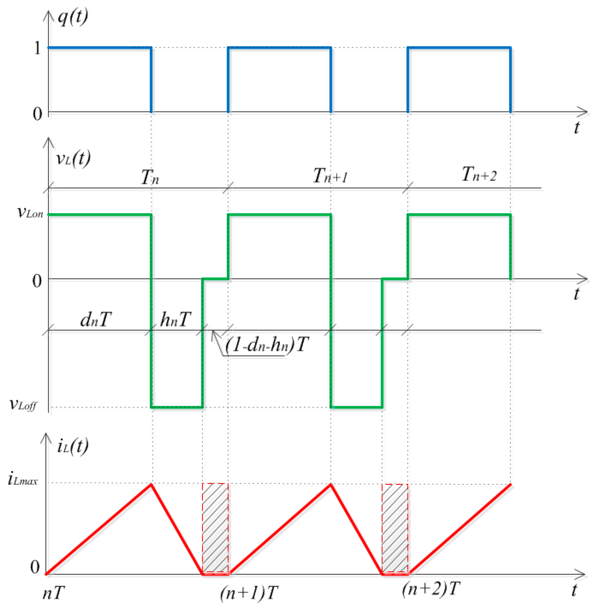
2. State-Space Description of the Discontinuous Conduction Mode

In the most general case, DCM is defined as the operation mode in which at least one asynchronous switching with respect to the control signals occurs. The passive switches, namely the diodes, are responsible for this type of operation. The main waveforms of a converter in DCM are depicted in Figure 1, where q(t) is the transistor switching function, dn is the duty cycle in the nth period, hnT is the length of the second topological state when the active switch is off and the diode is forward biased, and the third topological state is when both semiconductors are off. T is the switching period. Compared to CCM, in DCM a third topological state is introduced, corresponding to the hatched zone in Figure 1. Obviously, from Figure 1 it results that the lengths of the three topological states are dnT, hnT and (1 − dnhn)T for the on state, off state and the third state respectively.
In this paper the following notations have been adopted. Indexes of a discrete variable z obtained by sampling the continuous time variable z at the time moments nT are written as subscripts. For example zn = z(nT). The values of the continuous time variable at some time moment is denoted using rounded brackets, for example z(nT + dnT) is the value of the continuous variable z at the time moment nT + dnT. The state-space approach is used in this paper for converter description and analysis. As in each topological state a different linear time invariant (LTI) circuit is configured, a dc-dc converter is obviously a piecewise linear system.
The set of LTI equations that govern converter operation differ from one topological state to another. They can be written as:
{ d x d t = A 1 x ( t ) + B 1 u ( t )   when   t [ n T , ( n + d n ) T ) d x d t = A 2 x ( t ) + B 2 u ( t )   when   t [ ( n + d n ) T , ( n + d n + h n ) T ) d x d t = A 3 x ( t ) + B 3 u ( t )   when   t [ ( n + d n + h n ) T , ( n + 1 ) T )
where n is a positive integer, x(t) is the state vector, u(t) is the input vector containing the voltage sources and Ai, Bi, i = 1 , 3 ¯ , are the state matrices corresponding to the three topological states. In these conditions it is known [1,3] that converter operation can be described by the following discrete state equation:
x n + 1 = φ 3 φ 2 φ 1 x n + ( φ 3 φ 2 ψ 1 + φ 3 ψ 2 + ψ 3 ) u n
where the transition matrices involved in (2) are:
{ φ 1 = e A 1 d n T ;     ψ 1 = e A 1 d n T ( 0 d n T e A 1 τ d τ ) B 1 φ 2 = e A 2 h n T ;     ψ 2 = e A 2 ( d n + h n ) T ( d n T ( d n + h n ) T e A 2 τ d τ ) B 2 φ 3 = e A 3 ( 1 d n h n ) T ;     ψ 3 = e A 3 T ( ( d n + h n ) T T e A 3 τ d τ ) B 3
When matrices Ai are nonsingular, then ψ 1 , ψ 2 , ψ 3 can be written in a simplified form as:
{ ψ 1 = A 1 1 ( φ 1 I ) B 1 ψ 2 = A 2 1 ( φ 2 I ) B 2 ψ 3 = A 3 1 ( φ 3 I ) B 3
where I is the unity matrix of converter order. Even when singular, matrices ψ 1 , ψ 2 , ψ 3 can be easily evaluated from (3) using symbolic calculation. It is also important to remark that if Bi is a zero matrix, then the corresponding ψ i is also zero. This is the situation in the boost converter where B 3 = [ 0 0 ] t . More general, in any converter with the transistor connected in series with the supply voltage, matrices Bi are zero in all topological states when the transistor is off.
It is known that because of its periodic nature, the steady state solution of the discrete model is constant and therefore the duty cycles dn and hn are constant, denoted by D and H and the input vector un is also constant, U. Consequently, the steady-state transition matrices in (3) will be denoted by capitals as below:
{ Φ 1 = e A 1 D T ;     Ψ 1 = e A 1 D T ( 0 D T e A 1 τ d τ ) B 1 Φ 2 = e A 2 H T ;     Ψ 2 = e A 2 ( D + H ) T ( H T ( D + H ) T e A 2 τ d τ ) B 2 Φ 3 = e A 3 ( 1 D H ) T ;     Ψ 3 = e A 3 T ( ( D + H ) T T e A 3 τ d τ ) B 3
In these conditions the steady-state constant state vector X can be easily found from (2) imposing xn + 1 = xn = X, from which one obtains:
X = ( I Φ 3 Φ 2 Φ 1 ) 1 ( Φ 3 Φ 2 Ψ 1 + Φ 3 Φ 2 + Ψ 3 ) U

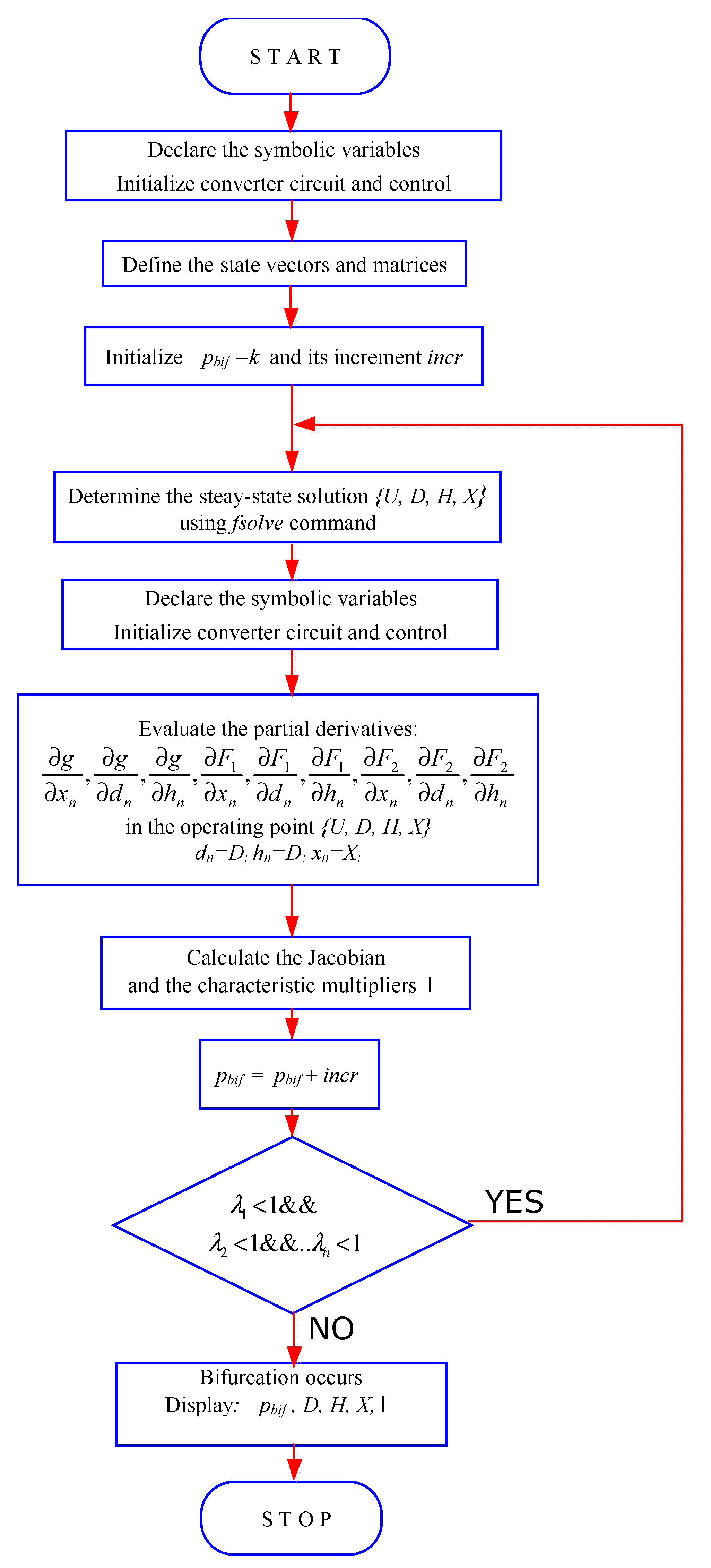
3. The New Method for Determining Bifurcation Parameter

Because the control of a dc-dc converter is of discrete nature, stability analysis can be performed if an iterative map of the form:
x n + 1 = f ( x n , u n , p b i f )
is available. Here pbif is a generic bifurcation parameter. The proposed approach is based on the small-signal assumption, requiring the determination of the Jacobian matrix J = f x n from (7) in a certain steady-state operating point (OP) {un = U, dn = D, xn = X} and the calculation of the eigenvalues (characteristic multipliers) from the well-known equation:
det ( λ I J ) = 0
However, in the most general case, the discrete state equation of a dc-dc converter is not of the form (7), but it can be written as:
x n + 1 = g ( x n , d n , h n , u n , p b i f )
Clearly the form of Equation (9) differs from Equation (7) because additional variables dn and hn appear. Comparing (2) to (9) it easily results that function g in (9) is:
g = φ 3 φ 2 φ 1 x n + ( φ 3 φ 2 ψ 1 + φ ψ 2 + ψ 3 ) u n
As previously mentioned, function g depends not only on xn and un, but also on dn and hn. This is due to the fact that matrices ϕi and ψ i , i = {1,2,3}, depend on dn and hn, as (3) reveals. It is clear that (10) is not an iterative map of the form (7), as the additional discrete variables dn and hn appear. However, the Jacobian can be still evaluated as will be described below, eliminating parameters dn and hn in the small-signal model, as they depend on xn and un. In order to achieve this let us first express the state vector at the end of the first and second topological states in terms of the state vector at the beginning of the corresponding topological state. Because in each of these states the circuit is LTI, this can be easily performed and one obtains:
x ( n T + d n T ) = φ 1 x ( n T ) + ψ 1 u n
x ( n T + d n T + h n T ) = φ 2 x ( n T + d n T ) + ψ 2 u n
In order to eliminate dn and hn from (9), two additional relationships are needed, both relating dn, xn, un, and possibly pbif. In the most general case, these equations are of the form
F 1 ( x n , d n , h n , u n , p b i f ) = 0
F 2 ( x n , d n , h n , u n , p b i f ) = 0
In any dc-dc converter Equation (13) is the control equation, (e.g., proportional voltage control, current mode control, charge control, etc.). Generally, function F1 is the result of a comparison between converter variables and reference magnitudes and F1 is not very complicated for most of control techniques. In this paper proportional voltage control is adopted as an example, but the reader can easily apply the principle to any type of control. In proportional voltage-mode control, illustrated in Figure 2 for a boost converter, the difference between the reference voltage Vref and the output voltage vc is amplified and then compared to a rising saw tooth signal vsaw. When amplified difference signal is higher than the saw tooth the transistor is switched on, otherwise it will be off. This is the so called natural sampling PWM control, but also uniform sampling can be used, that is when the output voltage is sampled at the beginning of each period and the value of the sample is provided to the control circuit. From the schematic in Figure 2 it results that transistor off switching occurs when:
v s a w ( n T + d n T ) = V U V L T d n T + V L = k [ V r e f v c ( n T + d n T ) ]
where VU, VL are the peak and the valley value of the sawtooth signal and k is the gain.
From (15) the discrete duty cycle is:
d n = k V u V L [ V r e f V e x v x ( n T + d n T ) ] V L V u V L
where the row vector Vexv extracts the capacitor voltage from state vector. As function F1 requires xn as argument, x ( n T + d n T ) has to be expressed in terms of xn. This is achieved substituting x ( n T + d n T ) from (11) in (16), resulting in:
d n = k V u V L [ V r e f V e x v ( φ 1 x ( n T ) + ψ 1 u n ) ] V L V u V L
From (17) function F1 is easily identified as:
F 1 ( x n , d n , h n , u n , p b i f ) = k { V r e f V e x v [ φ 1 x ( n T ) + ψ 1 u n ] } ( V u V L ) d n V L
Function F2 that appears in (14) typically describes the operation mode of the converter. In DCM it states that inductor current equals zero at the end of the second topological state. Mathematically this can be written as:
V e x i x ( ( n + d n + h n ) T ) = 0
where the vector Vexi is a row vector that extracts the inductor current from the state vector. Obviously, from (19) and (14) it follows that and intermediate form for of F2 is given by:
F 2 ( x n , d n , h n , u n , p b i f ) = V e x i x ( ( n + d n + h n ) T )
The final form of F2 is found substituting x((n + dn + hn)T) from successively substituting (11) in (12) and the result in (20), obtaining that:
F 2 ( x n , d n , h n , u n p b i f ) = V e x i [ φ 2 φ 1 x ( n T ) + ( φ 2 ψ 1 + ψ 2 ) u n ]
Concluding, in order to obtain an equation of the form (7) we have to eliminate dn and hn from the system of equations:
{ x n + 1 = g ( x n , d n , h n , u n , p b i f ) F 1 ( x n , d n , h n , u n , p b i f ) = 0 F 2 ( x n , d n , h n , u n p b i f ) = 0
where g, F1 and F2 are given by (10), (18) and (21) respectively. System (22) is in fact a generalized discrete state-space model, with two auxiliary variables represented by dn and hn and two constrains given by F1(xn, dn, hn, un, pbif) = 0 and F2(xn, dn, hn, un, pbif) = 0.
In most of the cases it is impossible to provide an explicit expression of type (7) for xn + 1 from (22). But as long as stability is of concern, local stability can be still exactly predicted. First it has to be stressed out that pbif is a parameter that influences the operating point and for local stability analysis it is a constant value. In the following, the symbol ^ will be used to denote the small-signal perturbations. Linearizing the three equations in (22) around the constant steady-state operating point defined by {U, D, H, X} and taking into account that p b i f = 0 because pbif is constant, one obtains:
{ x n + 1 = g x n | O P x n + g d n | O P d n + g h n | O P h n + g u n | O P u n F 1 x n | O P x n + F 1 d n | O P d n + F 1 h n | O P h n + F 1 u n | O P u n = 0 F 2 x n | O P x n + F 2 d n | O P d n + F 2 h n | O P h n + + F 2 u n | O P u n = 0
where in general the symbol z r | O P denotes the derivative of function z with respect to the variable r evaluated in the operating point.
As the model described by (23) is LTI, from its last two equations d n and h n can be expressed in terms of x n and u n , leading to the proposed mathematical model:
x n + 1 = ( g x n | O P + g d n | O P F 1 h n F 2 x n F 1 x n F 2 h n F 1 d n F 2 h n F 1 h n F 2 d n | O P + g h n | O P F 1 x n F 2 d n F 1 d n F 2 x n F 1 d n F 2 h n F 1 h n F 2 d n | O P ) x n + ( g u n | O P + g d n | O P F 1 h n F 2 u n F 1 u n F 2 h n F 1 d n F 2 h n F 1 h n F 2 d n | O P + g h n | O P F 1 u n F 2 d n F 1 d n F 2 u n F 1 d n F 2 h n F 1 h n F 2 d n | O P ) u n
From (24) the Jacobian J is easily identified as:
J = g x n | O P + g d n | O P F 1 h n F 2 x n F 1 x n F 2 h n F 1 d n F 2 h n F 1 h n F 2 d n | O P + g h n | O P F 1 x n F 2 d n F 1 d n F 2 x n F 1 d n F 2 h n F 1 h n F 2 d n | O P
Equation (25) is the final result that will be used in the analysis, where g F1 and F2 are defined by (9), (13) and (14) respectively in the general cases. For DCM operation the expressions of these functions are given by (10), (18) and (21) respectively. Examining (25) it can be seen that the partial derivatives of the functions g, F1 and F2 with respect to xn, dn and hn need be calculated. Also the exact steady-state operation point has to be calculated because the linearization process requires these derivatives to be evaluated in the steady-state operating point. This will be presented and performed in the next paragraph.

4. Partial Derivatives of Functions g, F1, F2 and Exact Steady-State Operating Point Calculation

For deriving the partial derivatives of function g evaluated in the operating point, Equation (10) is used. After some simple algebra the final result is:
g x n | O P = φ 3 φ 2 φ 1 | O P = Φ 3 Φ 2 Φ 1
g d n | O P = T Φ 3 ( Φ 2 Φ 1 A 1 A 3 Φ 2 Φ 1 ) X + T [ Φ 3 ( Φ 2 Φ 1 B 1 A 3 Φ 2 Ψ 1 ) ( Φ 3 A 3 Ψ 2 Φ 3 B 3 ) ] U
g h n | O P = T Φ 3 ( Φ 2 A 2 A 3 Φ 2 ) Φ 1 X + T [ Φ 3 ( Φ 2 A 2 A 3 Φ 2 ) Ψ 1 + Φ 3 ( Φ 2 B 2 A 3 Ψ 2 B 3 ) ] U
The partial derivatives of F1 evaluated in the operating point are straight from (18):
F 1 x n | O P = k V e x v Φ 1
F 1 d n | O P = k T V e x v ( A 1 Φ 1 X + Φ 1 B 1 U ) ( V u V L )
F 1 h n | O P = 0
Partial derivatives of F2 in the operating point are directly found from (21). The result is:
F 2 x n | O P = V e x v Φ 2 Φ 1
F 2 d n | O P = T V e x i Φ 2 Φ 1 ( A 1 X + B 1 U )
F 2 h n | O P = T V e x i Φ 2 [ A 2 Φ 1 X + ( A 2 Ψ 1 + B 2 ) U ]
In order to complete the Jacobian determination, the exact operating point needs to be calculated. This can be achieved using (6) and taking into account that in steady state the discrete model becomes a dc one, that is xn + 1 = xn = X, dn = D, hn = H and the steady-state transition matrices are those given by (5). It is obvious that X depends on D and H. The relative length D is found from (18) written for steady state, with dn = D. Thus a transcendent equation for D results in the form:
D + k [ V r e f V e x v ( Φ 1 X + Ψ 1 U ) ] = 0
After solving this equation, with D known, H is obtained in a similar way from (21) in steady state. The equation for finding H is:
V e x i [ Φ 2 Φ 1 X + ( Φ 2 Ψ 1 + Ψ 2 ) U ] = 0
In conclusion, first D is found from (35), then with D known H is found from (36) and finally X is given by (6). In other words, Equations (35), (36) and (6) constitute a nonlinear system that has to be numerically solved in order to obtain the steady state solution {D, H, X}, with U known.

5. Bifurcation Analysis Using the Proposed Mathematical Model

As an example how the theory developed can be applied, a Matlab™ bifurcation analysis is performed for a boost dc-dc converter employing proportional voltage-mode control, similar to that in Figure 2. As Figure 2 shows, parasitics for C and L are ignored although they can be any time included, as their presence only modify the state matrices without any influence on the algorithm.
The authors also performed simulations and experiments on high order converters, namely on the fourth order Sepic, Zeta and excellent agreement between theory, simulations and experiments was found. For the sake of simplicity and for space reasons only the results related to the Boost converter will be presented in the paper.
The bifurcation parameter pbif was chosen to be the amplifier gain k. Converter parameters are: Vg = 16 V; Vref = 22 V; C = 220 µF; T = 333.33 µs; R = 78 Ω; L = 1209 µH; Transistor on resistance is Ron = 0.2 Ω and diode forward voltage is VD = 0.4 V; Saw tooth parameters are VU = 3.5 V; VL = 0.7 V.
For the boost converter under study, choosing the state vector as x = [ i L v C ] t and U = [ V g V D ] t , the state matrices are:
A 1 = [ R o n L 0 0 1 R C ] ; A 2 = [ 0 1 L 1 C 1 R C ] ; A 3 = [ 0 0 0 1 R C ] ; B 1 = [ 1 L 0 0 0 ] ; B 2 = [ 1 L 1 L 0 0 ] ; B 3 = [ 0 0 0 0 ]
The program flow chart is presented in Figure 3. The MatlabTM code both for the main program BOOST_DCM.m and for the function f_system.m that is used with the fsolve command for calculating the dc operating point is provided in the Appendix A.
In Table 1 the evolution of the characteristic multipliers values as the bifurcation parameter k is progressively increased is presented. Four decimal places are retained as this is sufficient to provide the accuracy of the results with an at least 0.01%.
The increment for the bifurcation parameter was 1 × 10⁶. It can be remarked that one eigenvalue is always zero and this is explained by the fact that in DCM in any switching cycle the inductor current starts and ends at zero [10].
It can be remarked that at k = 1.1589 only one negative characteristic multiplier exits the unit circle. It is known that if a negative real eigenvalue moves out of the unit circle, while other eigenvalues are within the unit circle, the converter exhibits period-doubling bifurcation [2,10,11]. This prognosis will be confirmed by circuit simulation and experiments in the next paragraphs.

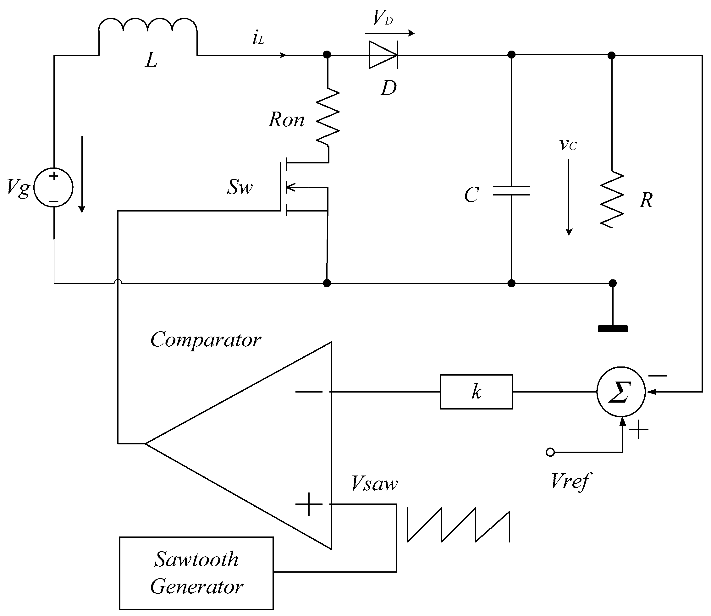
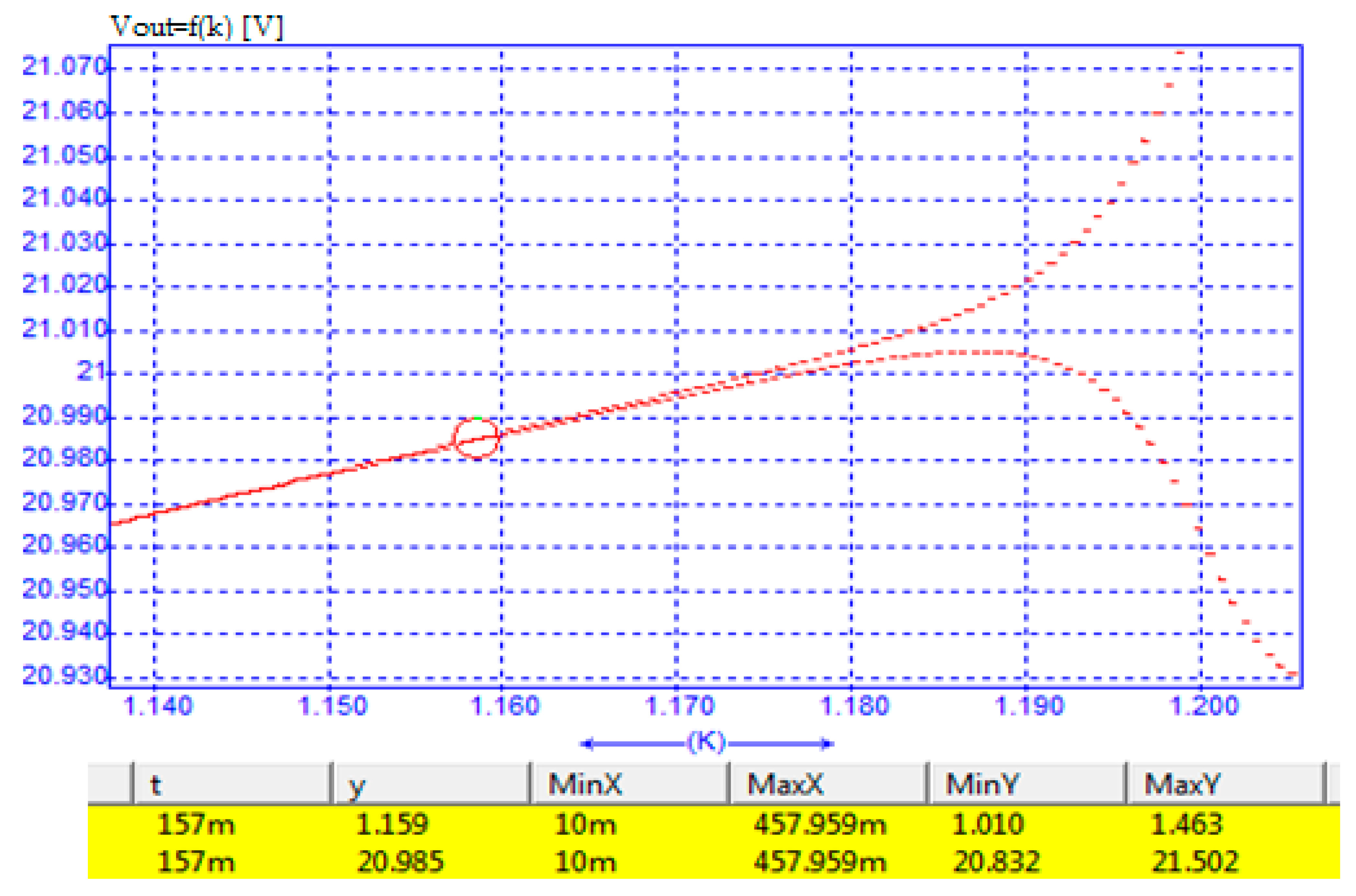
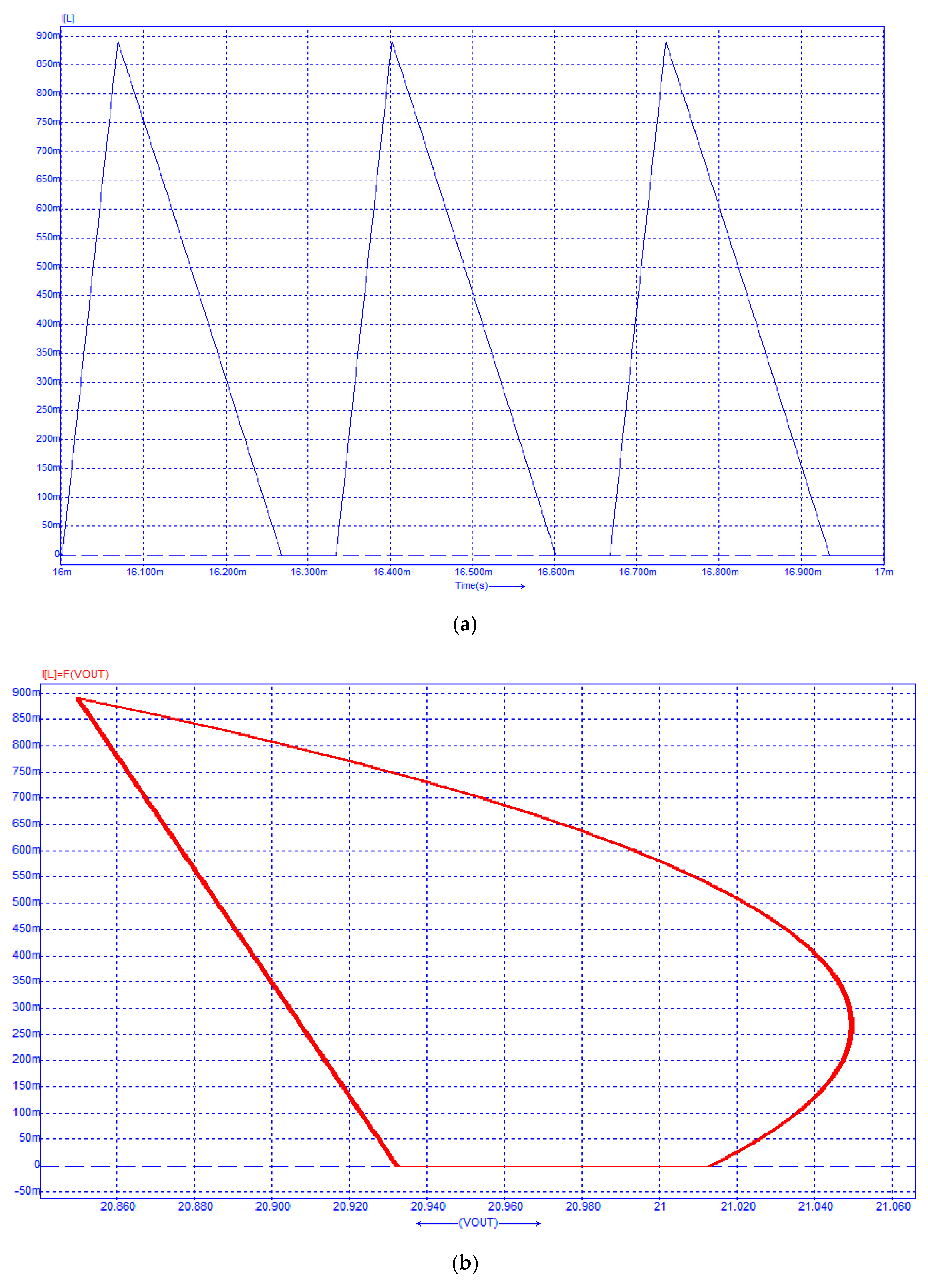
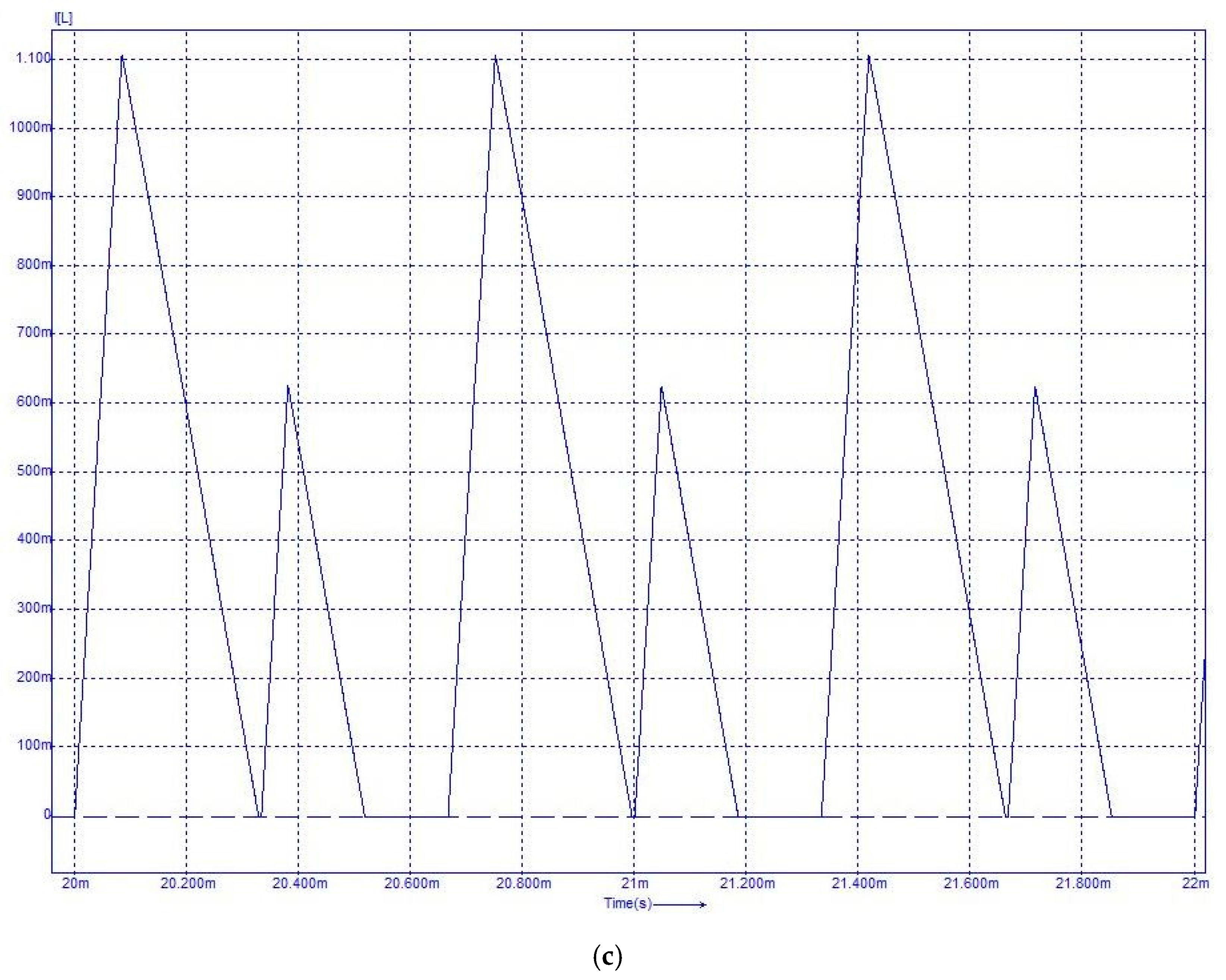
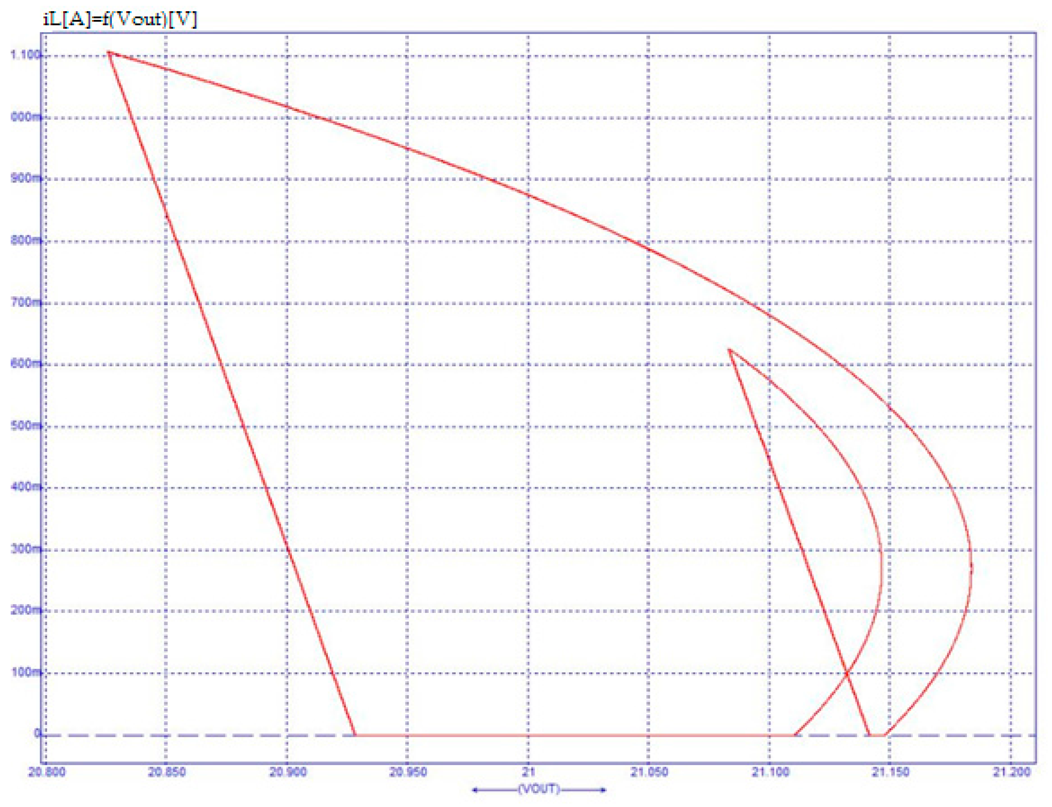
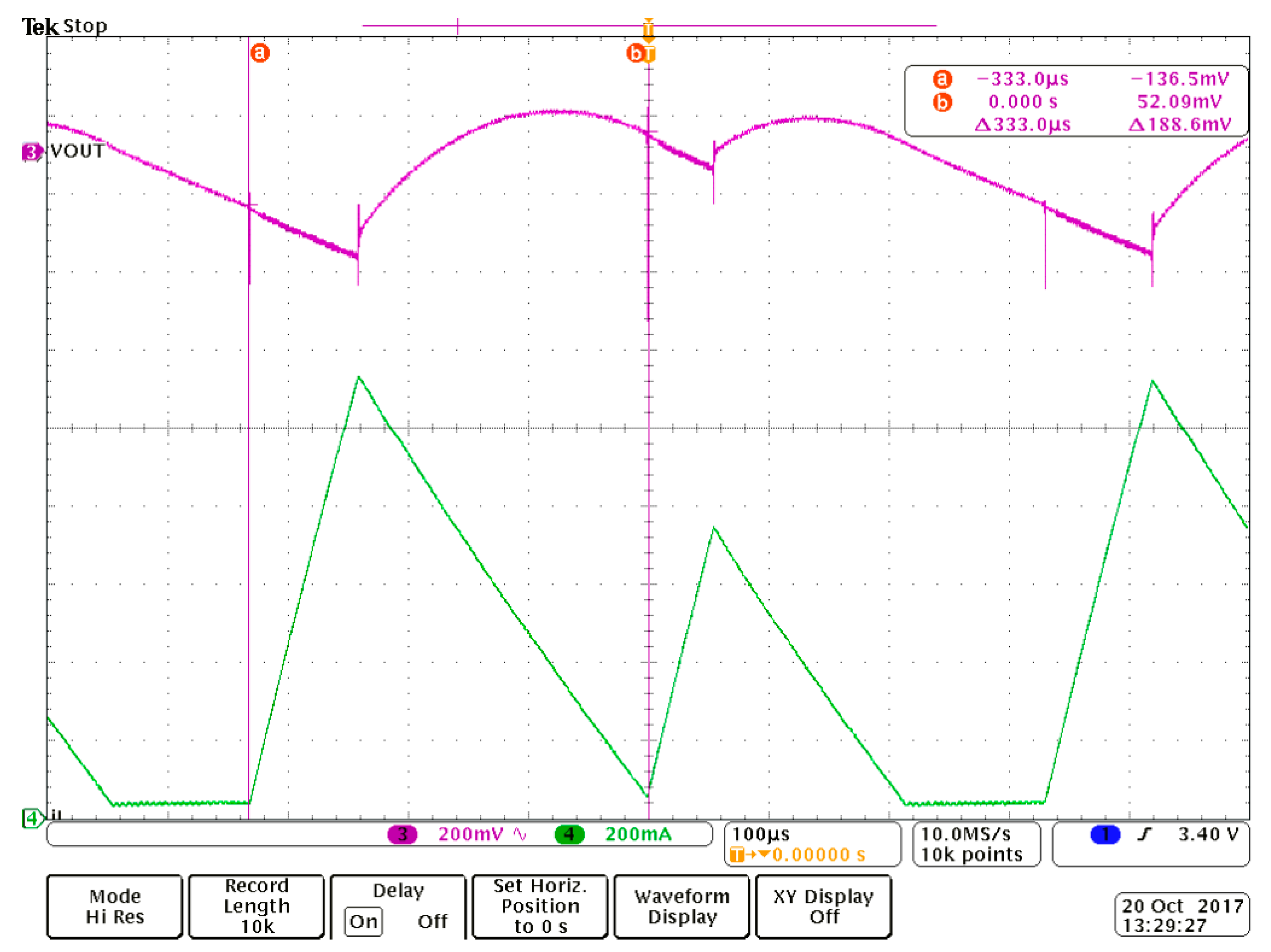
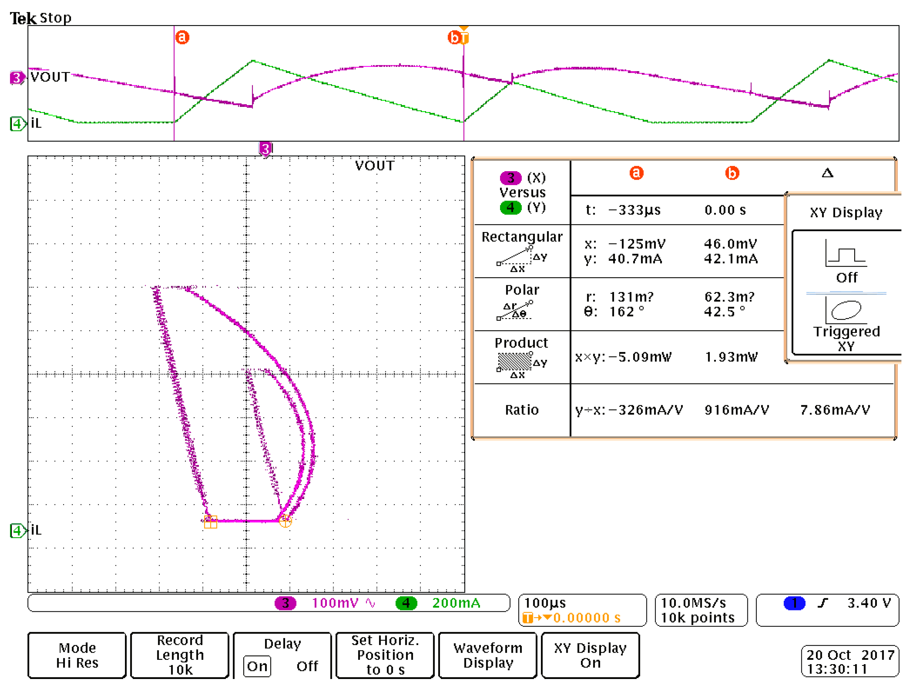
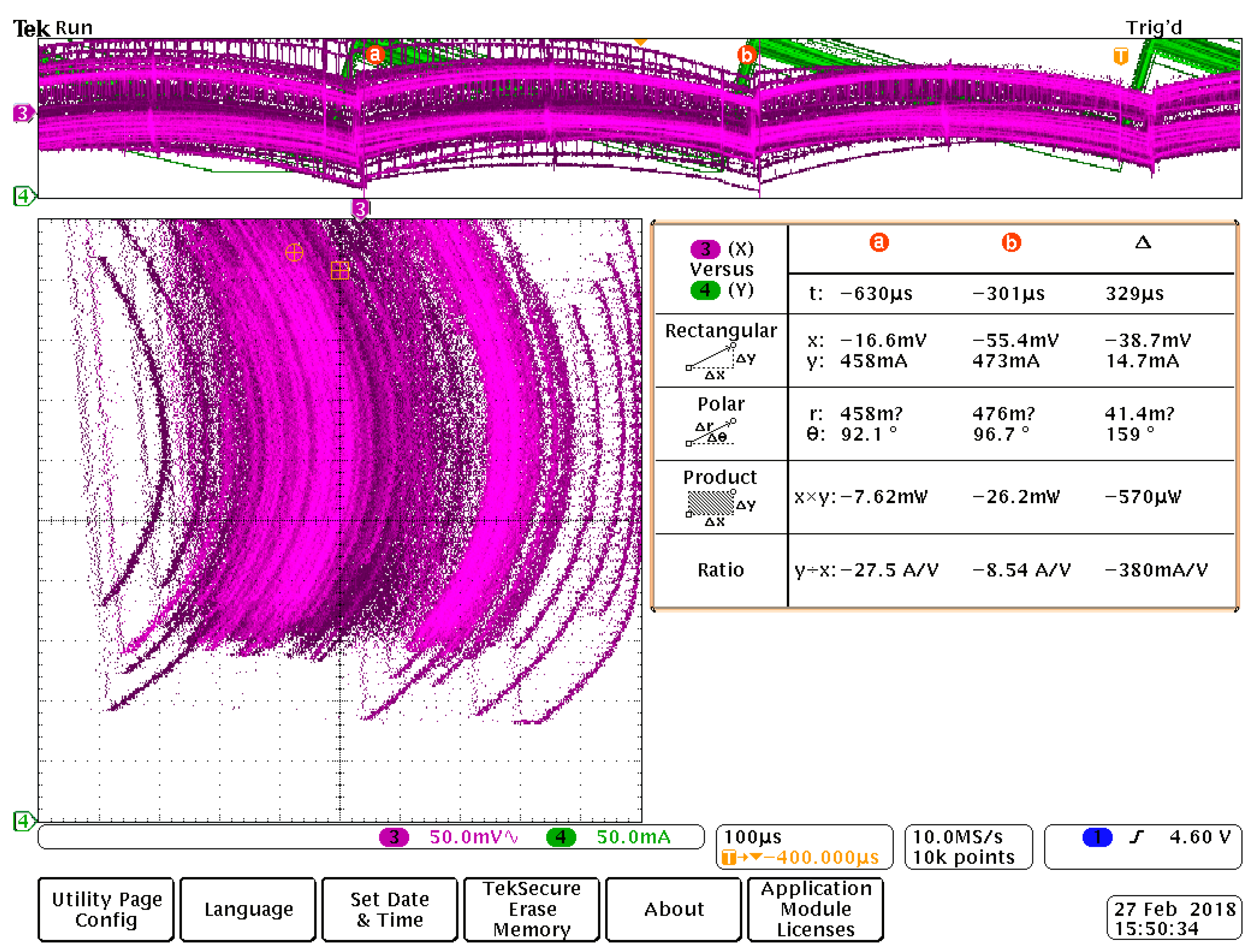
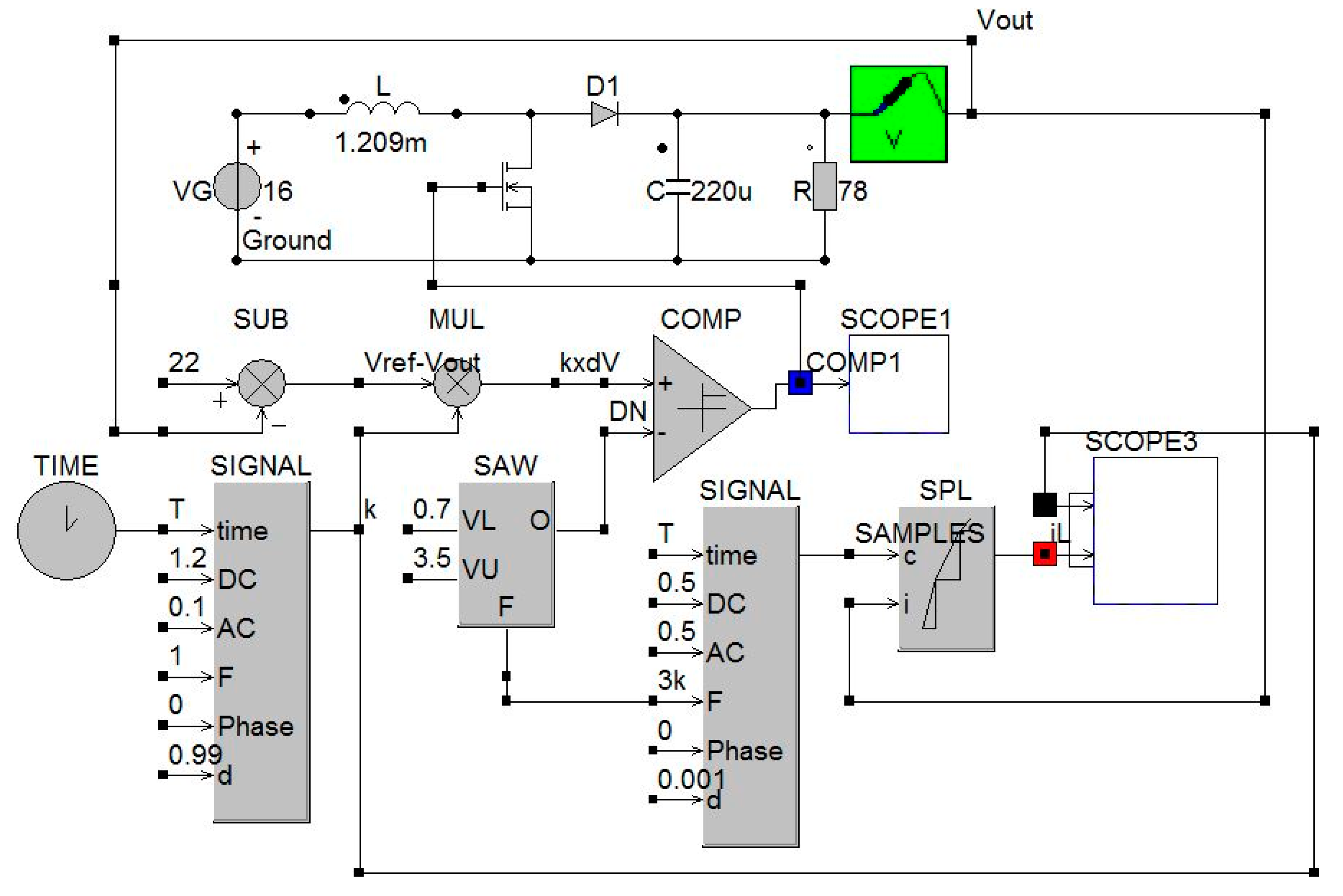
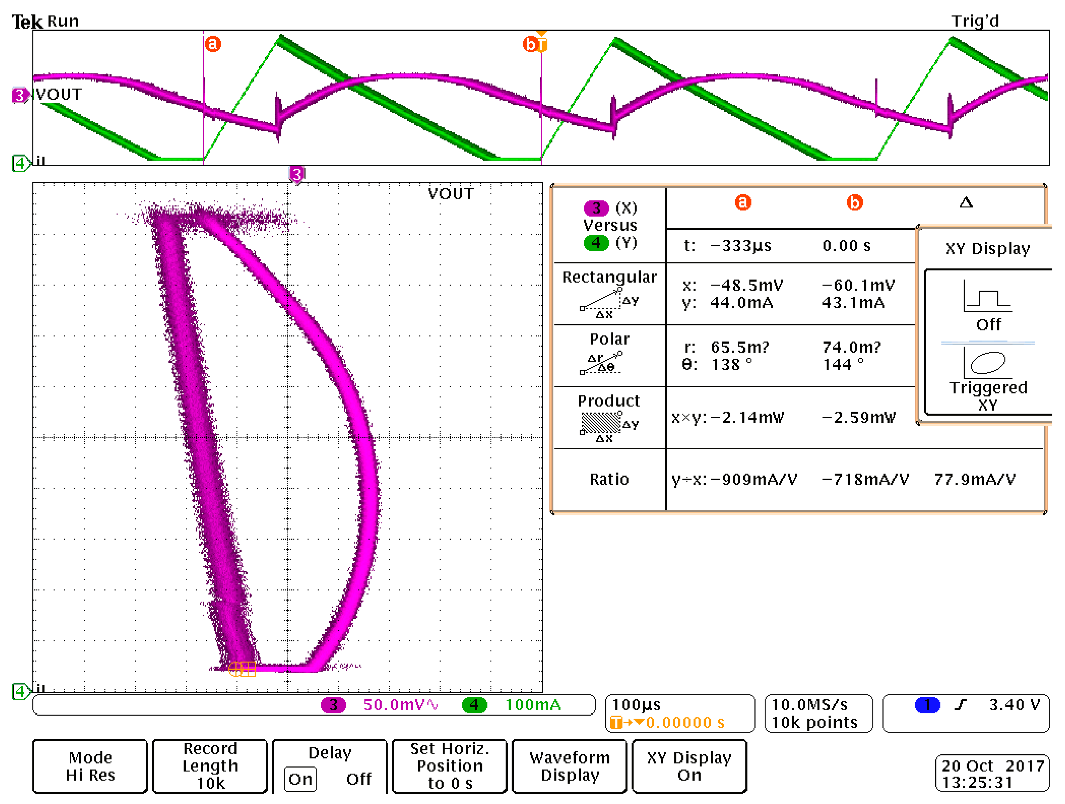
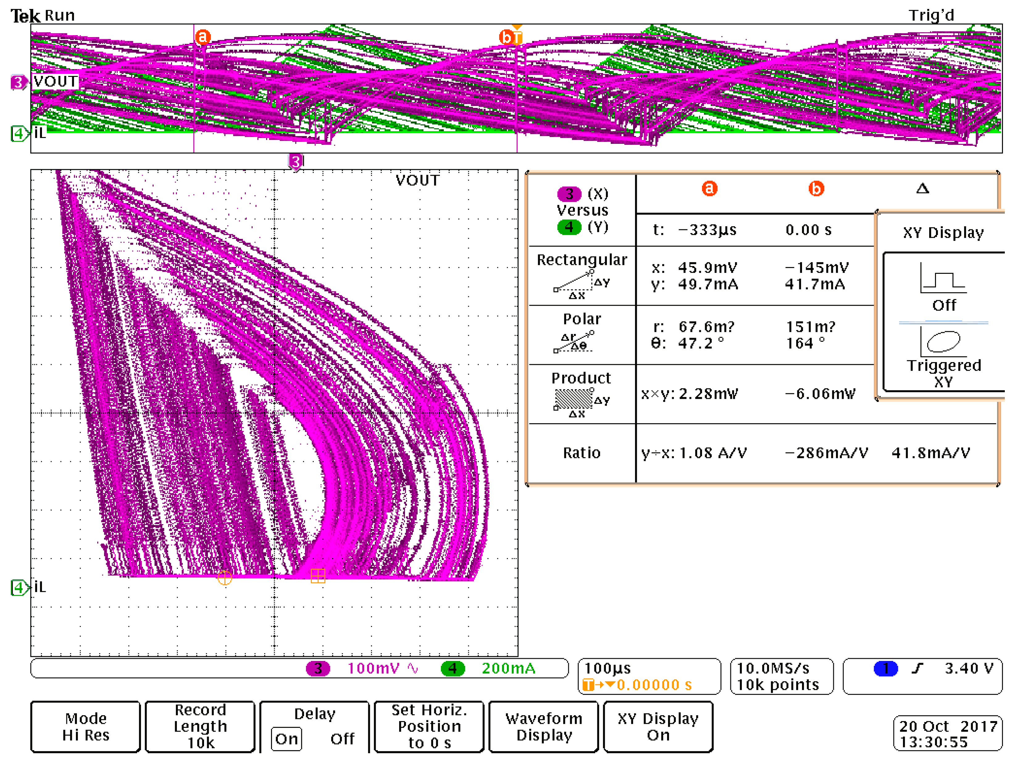
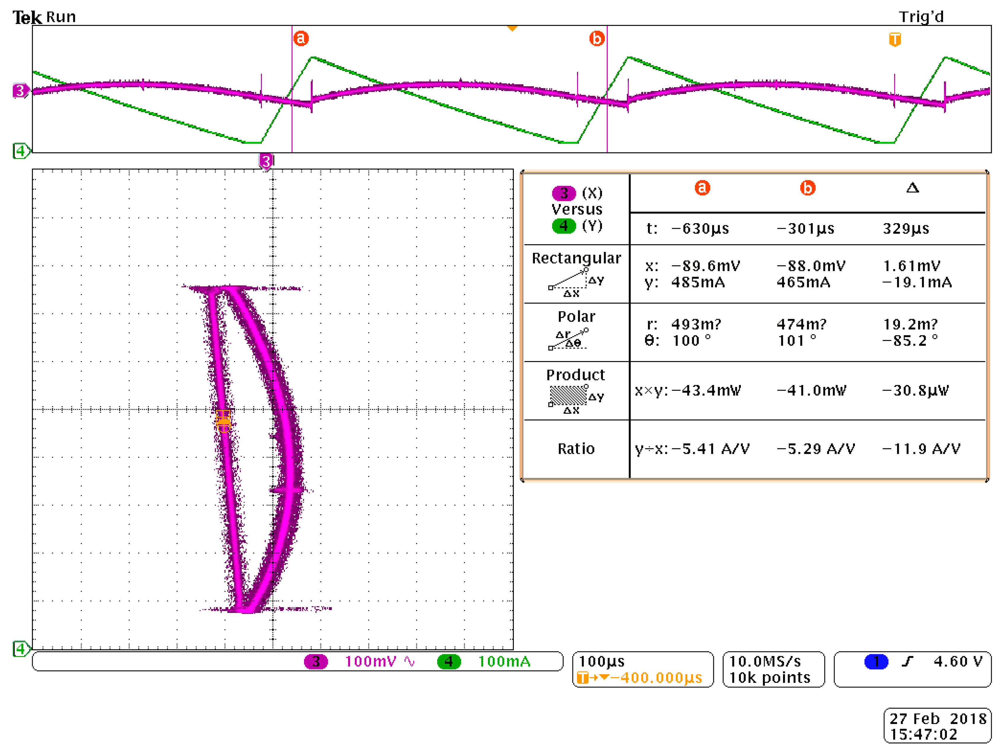
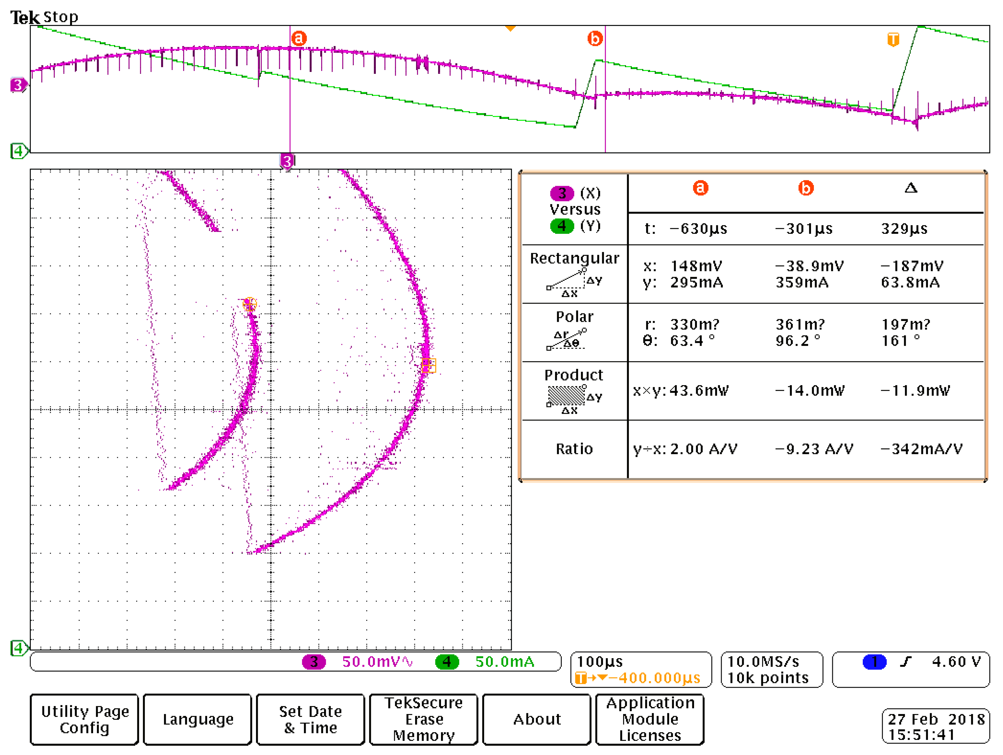
6. Validation through Circuit Simulation

In order to validate the theory developed and implemented in Matlab™, a circuit simulation is performed using the Caspoc™ package [17]. For correct results, the variation of the bifurcation parameter has to be very slow compared to converter dynamics, such that the operation to consist of a sequence of quasi steady-states, otherwise significant transients will occur and the bifurcation diagram will be altered. In our case k is varied from 1.1 to 1.2 in 1 s. The simulation schematic is presented in Figure 4. The bifurcation diagram is obtained in SCOPE3 displaying the values of k on the x axis and the sampled output voltage on the y axis.
The simulated bifurcation diagram obtained in SCOPE3 is enlarged presented in Figure 5, with a magnified image around the bifurcation point in Figure 6. The theoretical value of 1.159, marked with the red circle on the graph is the bifurcation threshold. In the small table below the Figure 6 the values in the column denoted by y represent voltage of the power supply and the output voltage values respectively, when the bifurcation appears.
From Figure 6 it can be seen that the first bifurcation with period doubling occurs at k = 1.159, which is an excellent agreement with the Matlab™ prognosis of 1.1589, with 0.092% relative error. In Figure 7a, a time representation of the inductor current in steady-state operation at a value of k = 1.1, lower than the bifurcation value is presented. In Figure 7b the phase portrait of the system for the same value of k is depicted.
Both representations in Figure 7a,b confirm that stable operation is achieved.
In Figure 7c, the inductor current waveform for a value of k = 1.2, a value that exceeds the bifurcation threshold, being located in the range where the bifurcation diagram prognoses a period doubling is enfaced. The corresponding phase portrait is shown in Figure 8. Figure 7c and Figure 8, reveal that period doubling occurs.
It can be remarked that still increasing k after the first bifurcation (for example for k = 1.215), period 4 bifurcation occurs. This bifurcation can also be numerically determined calculating the Jacobian of the function f(f), where f is the function in relationship (6). Obviously, the calculations are more complex, but the approach is the same as the one used for determining the period 2 bifurcation. Further increase of the bifurcation parameter causes the system to burst into chaos.

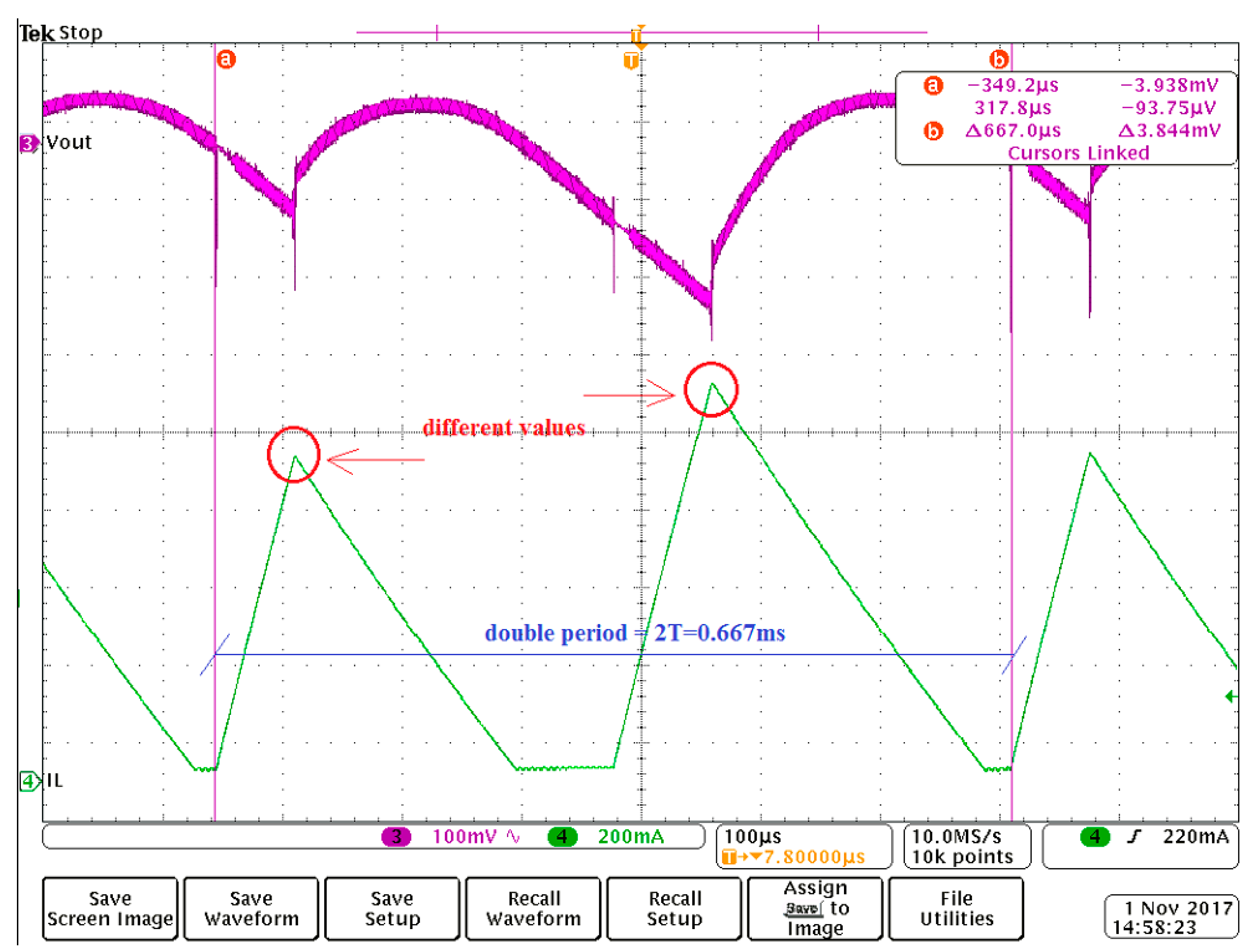
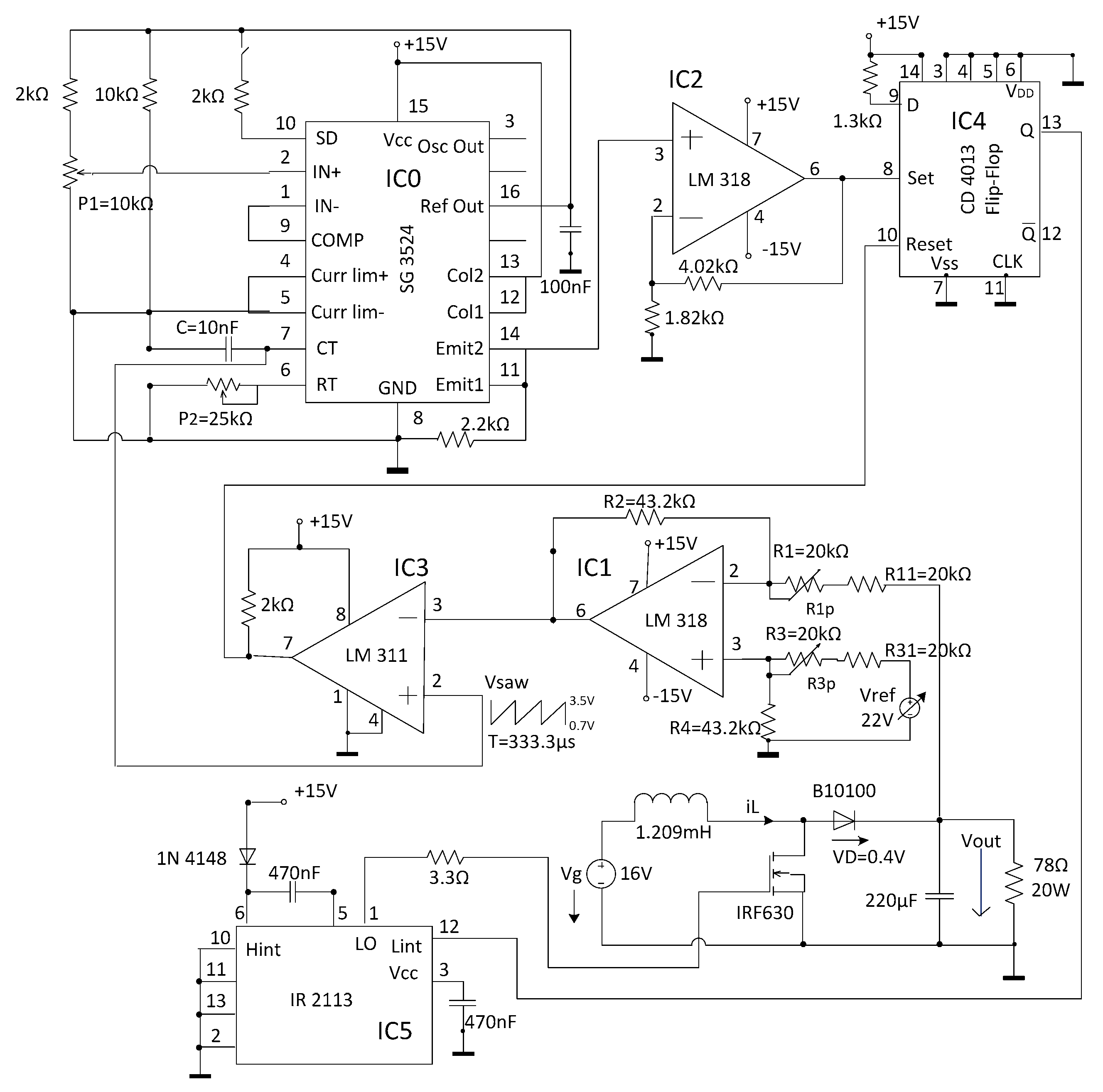
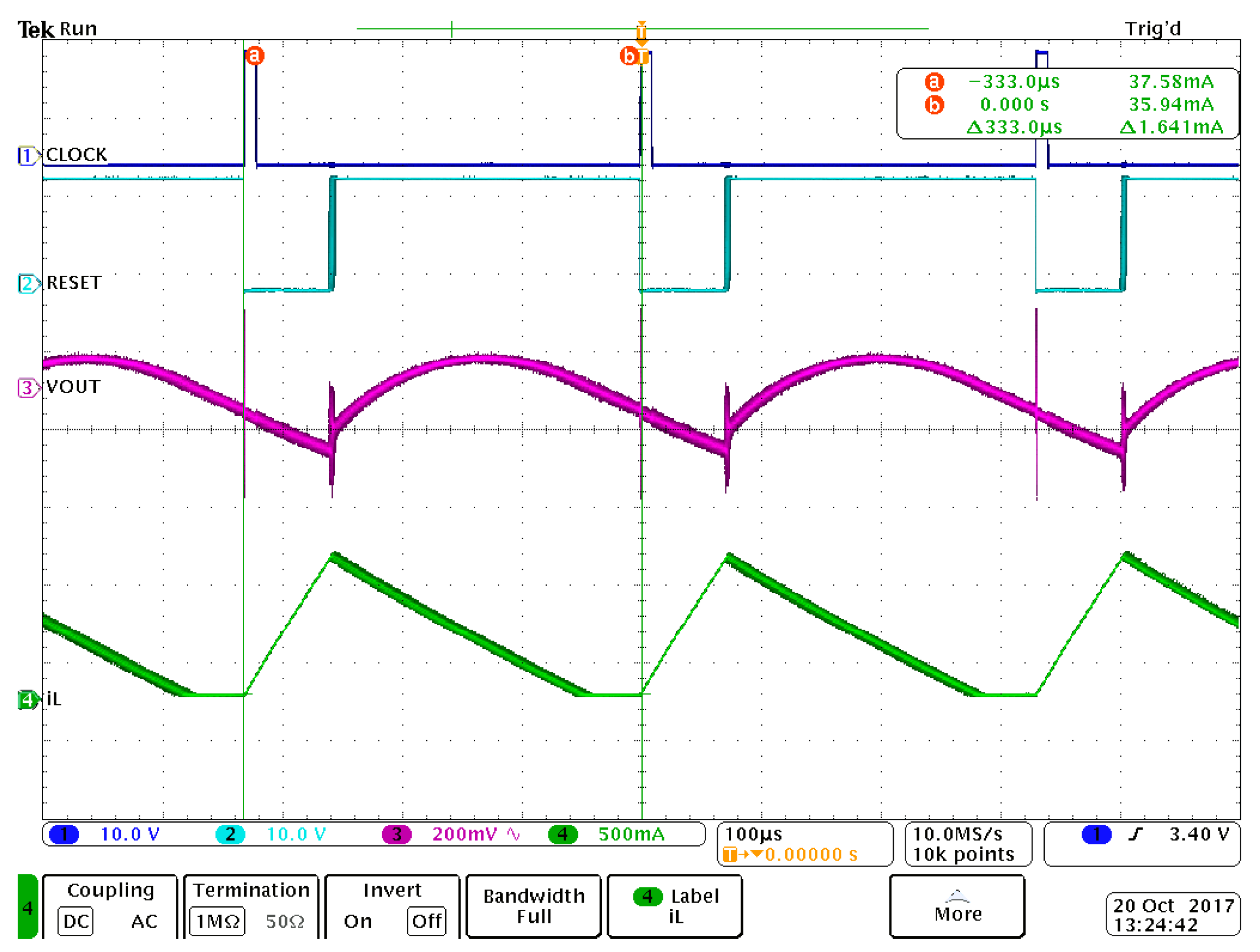
7. Experimental Results

The experimental setup schematic is presented in Figure 9. The differential amplifier consisting of IC1 and resistors R1 to R4 impose the value of the gain k. With the typical condition of the differential amplifier fulfilled, that is
R 2 ( R 1 p + R 11 ) = R 4 ( R 3 p + R 31 )
gain k is given by
k = R 2 R 11 + R 1 p = R 4 R 31 + R 3 p
For the values of the resistors used, k range is between 1.08 and 2.16. The saw tooth waveform is the voltage across capacitor C that together with potentiometer P2 imposes the operation frequency of the SG3524 represented by IC0 circuit and the switching frequency of the boost converter. The two outputs of the SG3524 circuit are connected in parallel, providing the short set pulses of the flip-flop. The pulse width is adjusted by potentiometer P1. IC2 is used to amplify the pulses such that to cross the threshold voltage of the flip-flop. The reset signal for the flip-flop is provided by the comparator represented by IC3. The switching frequency is 3 kHz, equal to that used in the simulation.
In Figure 10 system behavior for k = 1.08 is presented. The theory developed predicts stable operation both in Matlab™ and Caspoc™. This is experimentally confirmed by the waveforms in Figure 10, where all signals exhibit the switching period, with the typical DCM shape of the inductor current. The phase portrait is depicted in Figure 11, additionally confirming stable operation.
Then the gain factor k is then progressively increased and the inductor current is carefully monitored. When two consecutive periods differ it is decided that the system enters bifurcation and the corresponding value of k is retained. Figure 12 presents the inductor current and output voltage of the converter when the system goes from stable operation to bifurcation. It can be seen that two consecutive periods are not identical as the two inductor current peak values begin to slightly differ. The value of parameter k corresponding to this situation is k = 1.17, while the Matlab™ and Caspoc™ programs both predict that bifurcation appears at k = 1.16. Obviously, the relative error between the simulation and experiment is very low, equal to 0.94%. The error sources come from the fact that nonideal devices parameters, such as Ron and VD are not exactly known as only the catalog values were used and the series resistance of the inductor and capacitor were neglected. Other error sources are of course given by the equipment used but these are lower compared to those mentioned above. Thus the experimental result accurately validates the theoretical method proposed.
Further increasing the gain will reveal a more evident bifurcation. For example, in Figure 13 inductor current and output voltage are depicted for k = 1.20. The period of the system is clear half of the switching period (period 2 subharmonic) and the phase portrait enfaced in Figure 14 is typical for a period 2 bifurcation system.
A higher value of the gain will lead the converter into chaos. This situation is presented in Figure 15, both the waveforms and the phase portrait exhibiting the chaotic behavior.

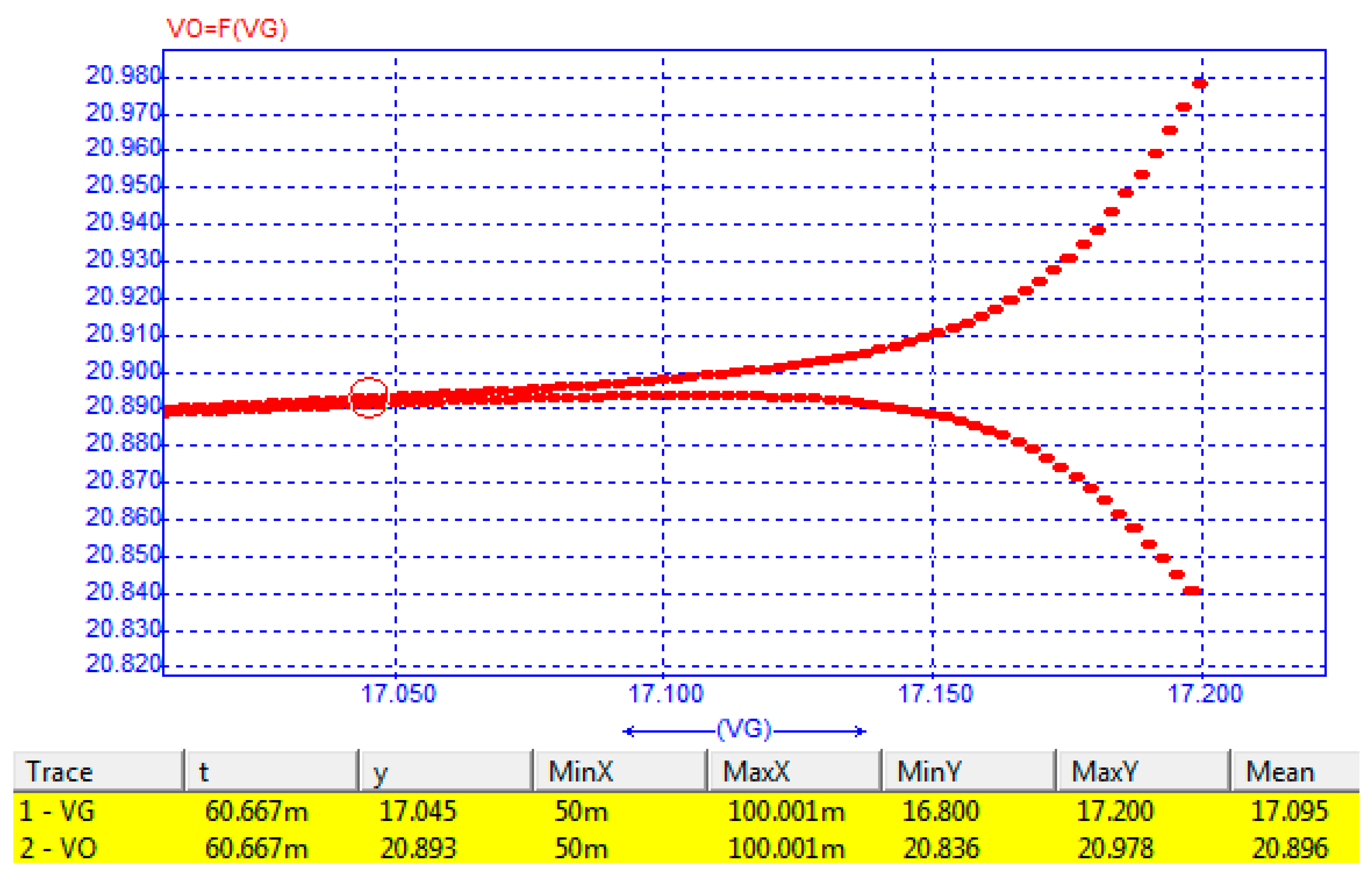
8. Input Voltage as a Bifurcation Parameter

In practice also the input voltage and the load resistance could affect the stability and the bifurcation behavior of a dc-dc. For this reason and in order to additionally prove the validity of the proposed method, a bifurcation analysis was carried out in the situation when the bifurcation parameter is the input voltage Vg. The value of the gain k is now kept constant and equal to 1.
In Table 2 the characteristic multipliers are depicted as the input voltage is gradually increased.
It can be seen that when Vg equals 17.125 V the bifurcation occurs. The Matlab program is in Appendix B.
Then the behavior of the converter was verified by Caspoc simulation. In Figure 16 the bifurcation diagram is presented, revealing the theoretical value of 17.045 V, marked with the red circle on the graph as the bifurcation threshold. In the small table below the Figure 16 the values in the column denoted by y represent voltage of the power supply and the output voltage values respectively, when the bifurcation appears. This value is in very good agreement with the theoretical one of 17.125 V (marked in the Table 2 with bold characters), with a relative error of 0.46%.
Finally the phenomena were experimentally confirmed. In Figure 17 the main waveforms and the phase portrait are presented for the situation of an input voltage of 16.5 V. This corresponds to a stable operation as the figure clearly presents.
In Figure 18 the behavior for an input voltage of 17.2 V, higher than the bifurcation threshold is depicted. The bifurcation phenomenon is obvious. Further increase of the input voltage will drive the system into chaos, as Figure 19 presents for an input voltage equal to 17.8 V.
Hence it can be concluded that the proposed method is valid, powerful and with a high degree of generality.

9. Conclusions

A new mathematical method for analyzing and predicting bifurcation behavior of DCM operated dc-dc converters is proposed. Compared to other methods this new approach performs exact calculation, without truncating any state matrix and thus correctly analyzing all the waveforms that in most of the approaches are approximated to be piecewise linear. On the other side, the new method is general, in the sense that it can be applied to any converter topology employing different types of control by simply changing only the matrices that describe the state-space model and one constraint equation. The proposed algorithm can be easily absorbed by any mathematical program that is able to calculate the matrix exponential. The method provides excellent accuracy, better than any other previous reported approach. The experimental results confirmed the perfect agreement between theory and practice. The proposed technique can also be used to exactly predict the parameter values that determine the operation at the border between DCM and CCM and thus to practically provide exact prediction of border collision. The method is different from those in [1,2,9,12,15] and can be also successfully applied both to uniform sampling and to different control techniques [15] employing CCM or other discontinuous modes, such as discontinuous capacitor voltage mode (DCVM) [18,19].

Author Contributions

All authors contributed to this research. Mircea Gurbina conceived and designed the study. Mircea Gurbina and Ioana-Monica Pop-Calimanu developed the Matlab programs and analyzed the data. Dan Lascu and Aurel Ciresan performed the Caspoc simulations. Ioana Pop and Septimiu Lica handled the experiments. Mircea Gurbina wrote the paper and managed all the correspondece with the editor. Dan Lascu reviewed the manuscript. All authors read and approved the final manuscript.

Conflicts of Interest

The authors declare no conflicts of interest.

Appendix A

BOOST_DCM.m
% Bifurcation and Chaos in DCM Boost Switching Regulators;
clear all; close all; clc;
% Declare symbolic variables
syms k x t Ron Vg D H R Rc C L T ;
format long
I=eye(2);Vexi=[1 0];Vexv=[0 1]; Vu=3.5; Vl=0.7;Vref=22;
Vg=16; C=220e-6; T=1000/3*1e-6; R=78; L=1.209e-3;Ron=0.2; Vd=0.4;U=[Vg;Vd];%
% Define de state and other necessary matrices and vectors
A1=[-Ron/L 0 ; 0 -1/(R*C)]; B1=[1/L 0; 0 0];
A2=[0 -1/L; 1/C -1/(R*C)];B2=[1/L -1/L; 0 0];
A3=[0 0 ; 0 -1/(R*C)]; B3=[0 0;0 0];
 k=1.1588; incr=0.0001; lambda=zeros(2);
while abs(lambda(1))<1 && abs(lambda(2))<1 % test whether both characteristic multipliers lie inside the unit circle
  % Determine the steady state solution for the duty cycles
  DandH=fsolve(@(x) f_sistem(x,k,t),[0.4;0.1]);
  D=DandH(1,1);H=DandH(2,1);
  % Calculate the actual matrices
  Phi1=expm(A1*D*T); Psi1=A1\(Phi1-I)*B1; %see system (3)
  Phi2=expm(A2*H*T); Psi2=A2\(Phi2-I)*B2; %see system (3)
  Phi3=expm(A3*(1-D-H)*T); Psi3=eval(expm(A3*T)*int(expm(-A3*t)*B3, t,(D+H)*T,T));%see system (3)
  % Calculate the actual steady-state state vector
  X=(I-Phi3*Phi2*Phi1)\((Phi3*Phi2*Psi1+Phi3*Psi2+Psi3)*U); %see Eq.6
  % Evaluate de partial derivatives
  dgdxn = Phi3*Phi2*Phi1;% see Eqn (26)
  dgddn = T*Phi3*(Phi2*Phi1*A1-A3*Phi2*Phi1)*X+T*Phi3*(Phi2*Phi1*B1-A3*Phi2*Psi1-A3*Psi2-B3)*U;% see Eqn (27)
  dgdhn = T*Phi3*(Phi2*A2-A3*Phi2)*Phi1*X+T*Phi3*((Phi2*A2-A3*Phi2)*Psi1+Phi2*B2-A3*Psi2-B3)*U;% see Eqn (28)
  dF1dxn = -k*Vexv*Phi1; % see Eqn (29)
  dF1ddn = -k*T*Vexv*(A1*Phi1*X+Phi1*B1*U)-(Vu-Vl); % see Eqn (30)
  dF1dhn = 0; %see Eqn (31)
  dF2dxn = Vexi*Phi2*Phi1; %see Eqn (32)
  dF2ddn = T*Vexi*Phi2*Phi1*(A1*X+B1*U);%see Eqn (33)
  dF2dhn = T*Vexi*Phi2*(A2*Phi1*X+(A2*Psi1+B2)*U); %see Eqn (34)
  % Calculate Jacobian (see Eqn (24))
  JFX=dgdxn+dgddn*(dF1dhn*dF2dxn-dF1dxn*dF2dhn)/(dF1ddn*dF2dhn-dF1dhn*dF2ddn)+dgdhn*(dF1dxn*dF2ddn-dF1ddn*dF2dxn)/(dF1ddn*dF2dhn-dF1dhn*dF2ddn);
  % Calculate the characteristic multipliers
  lambda=eig(JFX)
  lambda=abs(lambda);
  k=k+incr
  D,H
end
% Display the duty cycles, state vector, absolute value of characteristic
% multipliers and the critical value of the bifurcation parameter
lambda
k=k-incr, D, H, X
Function: f_system.m
function F=f_sistem(x,k,t)
I=eye(2);Vexi=[1 0];Vexv=[0 1];Vref=22;Vu=3.5; Vl=0.7;
Vg=16; C=220e-6; T=1000/3*1e-6; R=78; L=1.209e-3;Ron=0.2; Vd=0.4;U=[Vg;Vd];%
A1=[-Ron/L 0 ; 0 -1/(R*C)]; B1=[1/L 0; 0 0];
A2=[0 -1/L; 1/C -1/(R*C)];B2=[1/L -1/L; 0 0];
A3=[0 0 ; 0 -1/(R*C)]; B3=[0 0;0 0];
D=x(1);
H=x(2);
Phi1=expm(A1*D*T); Psi1=A1\(Phi1-I)*B1; %see system (3)
Phi2=expm(A2*H*T); Psi2=A2\(Phi2-I)*B2; %see system (3)
Phi3=expm(A3*(1-D-H)*T);Psi3=expm(A3*T)*int(expm(-A3*t)*B3, t,(D+H)*T,T);%see system (3)
F=zeros(2,1); % vector initialization
X=(I-Phi3*Phi2*Phi1)\((Phi3*Phi2*Psi1+Phi3*Psi2+Psi3)*U); %see Eq.6 %
F(1)=k*(Vref-Vexv*(Phi1*X+Psi1*U))-Vl-(Vu-Vl)*D; % see Eq.18
F(2)=Vexi*(Phi2*Phi1*X+(Phi2*Psi1+Psi2)*U);%see Eq.21
end

Appendix B

% Bifurcation and Chaos in DCM Boost Switching Regulators with the input voltage as a bifurcation parameter
clear all; close all; clc;
% Declare symbolic variables
syms k x t Ron Vg D H R Rc C L T ;
format long
I=eye(2);Vexi=[1 0];Vexv=[0 1]; Vu=3.5; Vl=0.7;Vref=22;
C=220e-6; T=1000/3*1e-6; R=78; L=1.209e-3;Ron=0.2; Vd=0.4;U=[Vg;Vd];k=1;%
% Define de state and other necessary matrices and vectors
A1=[-Ron/L 0 ; 0 -1/(R*C)]; B1=[1/L 0; 0 0];
A2=[0 -1/L; 1/C -1/(R*C)];B2=[1/L -1/L; 0 0];
A3=[0 0 ; 0 -1/(R*C)]; B3=[0 0;0 0];
Vg=16.8; incr=0.001; U=[Vg;Vd]; lambda=zeros(2);
while abs(lambda(1))<1 && abs(lambda(2))<1 % test whether both characteristic multipliers lie inside the unit circle
  % Determine the steady state solution for the duty cycles
  DandH=fsolve(@(x) f_sistem_Vg(x,Vg,t),[0.4;0.1]);
  D=DandH(1,1);H=DandH(2,1);
  % Calculate the actual matrices
  Phi1=expm(A1*D*T); Psi1=A1\(Phi1-I)*B1; %see system (3)
  Phi2=expm(A2*H*T); Psi2=A2\(Phi2-I)*B2; %see system (3)
  Phi3=expm(A3*(1-D-H)*T); Psi3=eval(expm(A3*T)*int(expm(-A3*t)*B3, t,(D+H)*T,T));%see system (3)
  % Calculate the actual steady-state state vector
  X=(I-Phi3*Phi2*Phi1)\((Phi3*Phi2*Psi1+Phi3*Psi2+Psi3)*U); %see Eq.6
  % Evaluate de partial derivatives
  dgdxn = Phi3*Phi2*Phi1;% see Eqn (26)
  dgddn = T*Phi3*(Phi2*Phi1*A1-A3*Phi2*Phi1)*X+T*Phi3*(Phi2*Phi1*B1-A3*Phi2*Psi1-A3*Psi2-B3)*U;% see Eqn (27)
  dgdhn = T*Phi3*(Phi2*A2-A3*Phi2)*Phi1*X+T*Phi3*((Phi2*A2-A3*Phi2)*Psi1+Phi2*B2-A3*Psi2-B3)*U;% see Eqn (28)
  dF1dxn = -k*Vexv*Phi1; % see Eqn (29)
  dF1ddn = -k*T*Vexv*(A1*Phi1*X+Phi1*B1*U)-(Vu-Vl); % see Eqn (30)
  dF1dhn = 0; %see Eqn (31)
  dF2dxn = Vexi*Phi2*Phi1; %see Eqn (32)
  dF2ddn = T*Vexi*Phi2*Phi1*(A1*X+B1*U);%see Eqn (33)
  dF2dhn = T*Vexi*Phi2*(A2*Phi1*X+(A2*Psi1+B2)*U); %see Eqn (34)
  % Calculate Jacobian (see Eqn (24))
  JFX=dgdxn+dgddn*(dF1dhn*dF2dxn-dF1dxn*dF2dhn)/(dF1ddn*dF2dhn-dF1dhn*dF2ddn)+dgdhn*(dF1dxn*dF2ddn-dF1ddn*dF2dxn)/(dF1ddn*dF2dhn-dF1dhn*dF2ddn);
  % Calculate the characteristic multipliers
  lambda=eig(JFX)
  lambda=abs(lambda);
  Vg=Vg+incr
  D,H
end
% Display the duty cycles, state vector, absolute value of characteristic
% multipliers and the critical value of the bifurcation parameter
lambda
Vg=Vg-incr, D, H, X
function F=f_sistem(x,Vg,t)
I=eye(2);Vexi=[1 0];Vexv=[0 1];Vref=22;Vu=3.5; Vl=0.7;
k=1; C=220e-6; T=1000/3*1e-6; R=78; L=1.209e-3;Ron=0.2; Vd=0.4;U=[Vg;Vd];%
A1=[-Ron/L 0 ; 0 -1/(R*C)]; B1=[1/L 0; 0 0];
A2=[0 -1/L; 1/C -1/(R*C)];B2=[1/L -1/L; 0 0];
A3=[0 0 ; 0 -1/(R*C)]; B3=[0 0;0 0];
D=x(1);
H=x(2);
Phi1=expm(A1*D*T); Psi1=A1\(Phi1-I)*B1; %see system (3)
Phi2=expm(A2*H*T); Psi2=A2\(Phi2-I)*B2; %see system (3)
Phi3=expm(A3*(1-D-H)*T);Psi3=expm(A3*T)*int(expm(-A3*t)*B3, t,(D+H)*T,T);%see system (3)
F=zeros(2,1); % vector initialization
X=(I-Phi3*Phi2*Phi1)\((Phi3*Phi2*Psi1+Phi3*Psi2+Psi3)*U); %see Eq.6 %
F(1)=k*(Vref-Vexv*(Phi1*X+Psi1*U))-Vl-(Vu-Vl)*D; % see Eq.18
F(2)=Vexi*(Phi2*Phi1*X+(Phi2*Psi1+Psi2)*U);%see Eq.21
end

Nomenclature

Main Symbols

Ai, BiState matrices
VDDiode voltage
vsawSawtooth signal
RiResistor
kGain
VrefReference voltage
VU, VLThe peak and the valley value of the sawtooth signal
q(t)Transistor switching function
vL(t)Inductor voltage
vc(t)Output voltage
iL(t)Inductor current
dnDuty cycle
hnTSecond state
(1dnhn)TThird state
u(t)Input vector
DDc duty cycle
HDc on state of diode
XSteady state vector
UDc input vector
VgInput voltage
T, Tn, Tn + 1Switching period
VexvExtracts the capacitor voltage from state vector
CCapacitor
LInductor
RonTransistor on resistance
PiPotentiometer
VgSecond state and the third state respectively
x(t)State vector
VoutOutput voltage

Abbreviations

PWMPulsed width modulated
ICiIntegrated circuits
OPOperating point
SUBSubstract
MULMultiplicator
SIGNALSignal generator
TIMEClock signal
SPLSample and Hold
DCMDiscontinuous conduction mode
CCMContinuous conduction mode
CMPTCurrent-mode pulse train
LTILinear time invariant

Greek Symbols

φ i , ψ i Transfer matrices
λEigenvalue

References

  1. Tse, C.-K. Complex Behavior of Switching Power Converters, 1st ed.; CRC Press: Boca Raton, FL, USA; London, UK; New York, NY, USA; Washington, DC, USA, 2003; pp. 91–106. [Google Scholar]
  2. Banerjee, S.; Verghese, G.C. Nonlinear Phenomena in Power Electronics, 1st ed.; IEEE Press: New York, NY, USA, 2001; pp. 25–52. [Google Scholar]
  3. Banerjee, S.; Chakrabarty, K. Nonlinear modeling and bifurcations in the boost converter. IEEE Trans. Power Electron. 1998, 13, 252–260. [Google Scholar] [CrossRef]
  4. Fang, C.-C.; Abed, E.-H. Sampled-Data Modeling and Analysis of PWM DC-DC Converters Part I. Closed-Loop Crcuits; Office of Naval Research: Arlington, TX, USA, 1998. [Google Scholar]
  5. Gurbina, M.; Draghici, D.; Ciresan, A.; Lascu, D. A New General Mathematical Technique for Stability and Bifurcation Analysis of DC-DC Converters Applied to One-Cycle Controlled Buck Converters with Non-Ideal Reset; Optimization of Electrical and Electronic Equipment (OPTIM): Bran, Romania, 2014; pp. 576–581. [Google Scholar]
  6. Gurbina, M.; Lica, S.; Lascu, D. Stability and bifurcation aspects in charge controlled DC-DC converters. In Proceedings of the 11th International Symposium on Electronics and Telecommunications (ISETC), Timisoara, Romania, 14–15 November 2014; pp. 1–4. [Google Scholar]
  7. Aroudi, A. A New Approach for Accurate Prediction of Subharmonic Oscillation in Switching Regulators—Part I: Mathematical Derivations. IEEE Trans. Power Electron. 2017, 32, 5651–5665. [Google Scholar] [CrossRef]
  8. Aroudi, A. A New Approach for Accurate Prediction of Subharmonic Oscillation in Switching Regulators—Part II: Case Studies. IEEE Trans. Power Electron. 2017, 32, 5835–5848. [Google Scholar] [CrossRef]
  9. Zhang, X.; Xu, J.; Bao, B.; Zhou, G. Asynchronous-switching map-based stability effects of circuit parameters in fixed off-time controlled buck converter. IEEE Trans. Power Electron. 2016, 31, 6686–6697. [Google Scholar] [CrossRef]
  10. Parui, S.; Banerjee, S. Bifurcations due to transition from continuous conduction mode to discontinuous conduction mode in the boost converter. IEEE Trans. Circuits Syst. I 2003, 50, 1464–1469. [Google Scholar] [CrossRef]
  11. Tse, C.-K. Chaos from a buck switching regulator operating in discontinuous mode. Int. J. Circuit Theory Appl. 1994, 22, 263–278. [Google Scholar] [CrossRef]
  12. Vilamitjana, E.; Aroudi, A.; Alarcon, E. Chaos in Switching Converters for Power Management. Designing for Prediction and Control; Springer: Berlin, Germany, 2013; pp. 31–38. [Google Scholar]
  13. Xie, F.; Yang, R.; Zhang, B. Bifurcation and border collision analysis of voltage-mode-controlled flyback converter based on total ampere-turns. IEEE Trans. Circuits Syst. I 2011, 58, 2269–2280. [Google Scholar] [CrossRef]
  14. Xuesong, F.; Chuang, B.; Yong, X.; Qian, Z. Dynamical Analysis of the DCM Buck Converter; Communications, Circuits and Systems (ICCCAS): Chengdu, China, 2013; pp. 442–445. [Google Scholar]
  15. Jin, S.; Jianping, X.; Bocheng, B. Effects of circuit parameters on dynamics of current-mode-pulse-train-controlled buck converter. IEEE Trans. Ind. Electron. 2014, 61, 1562–1573. [Google Scholar]
  16. Parui, S.; Basak, B. Inherent oscillation in Cuk converter and its effect on bifurcation phenomena. In Proceedings of the TENCON 2014 IEEE Region 10 Conference, Bangkok, Thailand, 22–25 October 2014; pp. 1–6. [Google Scholar]
  17. CASPOC. User Manual. Available online: http://www.simulation-research.com (accessed on 11 January 2018).
  18. Ivan, C.; Lascu, D.; Popescu, V. Hopf Bifurcation in a Discontinuous Capacitor Voltage Mode Ćuk dc-dc Converter. In Proceedings of the 6th WSEAS International Conference on Instrumentation, Measurement, Circuits and Systems, Hangzhou, China, 15–17 April 2007; pp. 78–83. [Google Scholar]
  19. Suntiom, T. Unified average and small-signal modeling of direct-on-time control. IEEE Trans. Ind. Electron. 2006, 53, 287–295. [Google Scholar] [CrossRef]
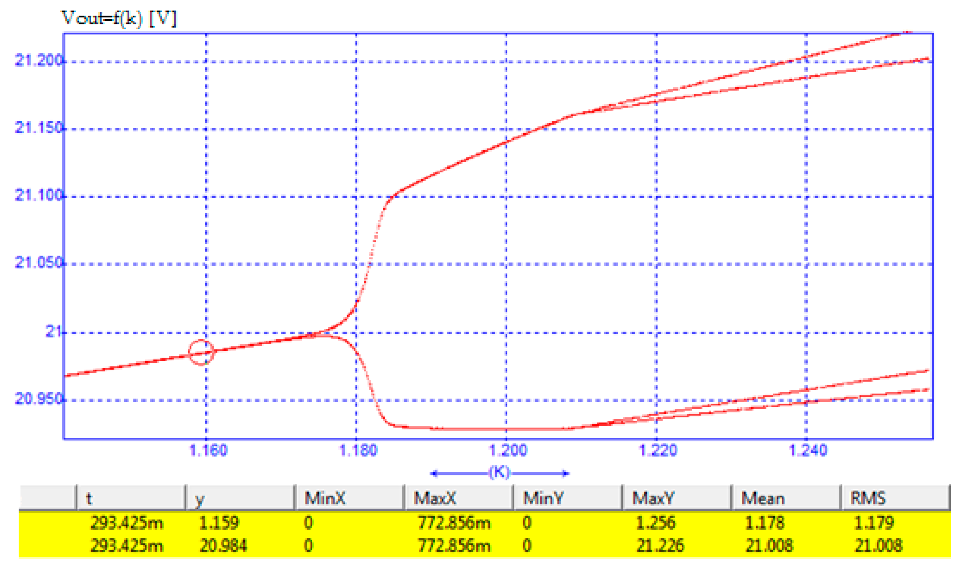
Figure 1. Transistor switching function, inductor voltage and inductor current in a DCM operated dc-dc converter.
Energies 11 00663 g001
Figure 2. Proportional voltage-mode controlled boost converter.
Energies 11 00663 g002
Figure 3. Flow chart of the Matlab™ program for determining the critical bifurcation parameter value.
Energies 11 00663 g003
Figure 4. Caspoc™ schematic for the proportional voltage-mode controlled boost converter.
Energies 11 00663 g004
Figure 5. The simulated bifurcation diagram of the boost DCM converter employing proportional voltage-mode control.
Energies 11 00663 g005
Figure 6. Magnified image around the bifurcation point. Clearly bifurcation appears at k = 1.159. The table below provides the instantaneous values of the simulated waveforms, together with their minimum and maximum values.
Energies 11 00663 g006
Figure 7. (a) The inductor current waveform for k = 1.1. The horizontal dotted line denotes the zero level and the solid line the inductor current. (b) Phase portrait for stable operation, k = 1.1. (c) Inductor current for parameter k = 1.2, higher than bifurcation threshold value of 1.1589. Unstable operation with period doubling (period 2 subharmonic) is obvious.
Energies 11 00663 g007aEnergies 11 00663 g007b
Figure 8. Phase portrait for k = 1.2, higer than 1.1589, confirming period doubling.
Energies 11 00663 g008
Figure 9. Schematic of the experimental boost DCM converter employing proportional voltage-mode control.
Energies 11 00663 g009
Figure 10. Set signal and reset signals of IC4, inductor current and output voltage waveform (this up to down order) for k = 1.08. Stable operation can be remarked.
Energies 11 00663 g010
Figure 11. Phase portrait for k = 1.08, confirming stable operation.
Energies 11 00663 g011
Figure 12. Inductor current and output voltage waveforms for k = 1.17. Notice that the peak inductor current values start to slightly differ in two consecutive periods and the period of the inductor current doubles compared to stable operation.
Energies 11 00663 g012
Figure 13. Inductor current and output voltage waveforms for k = 1.20. Bifurcation with period 2 operation is evident.
Energies 11 00663 g013
Figure 14. Phase portrait for k = 1.20, clearly revealing period 2 operation.
Energies 11 00663 g014
Figure 15. Chaotic operation of the converter corresponding to k = 1.50.
Energies 11 00663 g015
Figure 16. The simulated bifurcation diagram of the boost DCM converter: Vout = f(Vg).
Energies 11 00663 g016
Figure 17. Phase portrait for Vg = 16.50 V, confirming stable operation.
Energies 11 00663 g017
Figure 18. Phase portrait for Vg = 17.20, clearly revealing period 2 operation.
Energies 11 00663 g018
Figure 19. Chaotic operation of the converter corresponding to Vg = 17.80 V.
Energies 11 00663 g019
Table 1. Characteristic multipliers of the boost converter for increasing values of the gain k. The bold value in the first column denotes the threshold when bifurcation occurs.
Gain kEingenvalue l1Eingenvalue l2Remark
1.1560−0.99450.0000stable
1.1570−0.99640.0000stable
1.1580−0.99830.0000stable
1.1589−1.00000.0000Bifurcation
1.1600−1.00200.0000Bifurcation
1.2000−1.07750.0000Bifurcation
1.3000−1.27150.0000Bifurcation
Table 2. Characteristic multipliers of the boost converter for increasing values of the voltage Vg. The bold value in the first column denotes the threshold when bifurcation occurs.
Voltage VgEingenvalue l1Eingenvalue l2Remark
16.6000−0.86230.0000stable
16.8000−0.89830.0000stable
17.0000−0.97510.0000stable
17.1250−1.00000.0000Bifurcation
17.2000−1.01380.0000Bifurcation
17.4000−1.05720.0000Bifurcation
17.6000−1.10400.0000Bifurcation

