1. Introduction
At present, Hybrid Storage Systems (HSSs) are turning into one of the key technologies in power electronics related disciplines [
1]. Indeed, by using these systems, there is a reported improvement in the performance at leading applications such as integration in the distribution network of stochastic power generators [
2,
3], grid stability and power quality support upon line contingencies [
4], management of fast dynamics high power loads at the power-train in electric-hybrid vehicles [
5,
6], and a manifold of industrial applications with a load profile of large transient characteristics [
7], among others. Generally speaking, these HSSs interface a fast-dynamics high-power storage device, e.g., a Ultracapacitor Module (UM), with a slower, bulk-energy storage unit, e.g., an Electrochemical Battery (EB) [
8]. The design of the HSS involves the selection of adequate energy and power ratings in the elements of the system, as well as the design of a control scheme that manages properly the involved power flows [
9]. The final design must ensure that the resulting HSS shows an overall enhanced performance, providing the energy ratings of the main energy storage device, but simultaneously maintaining the power ratings of the fast-dynamics one [
1,
10,
11,
12]. The management of the power flows in the system is generally implemented through Power Electronic Converters (PEC) that enable synchronized control and operation of the involved storage units [
10,
11,
12].
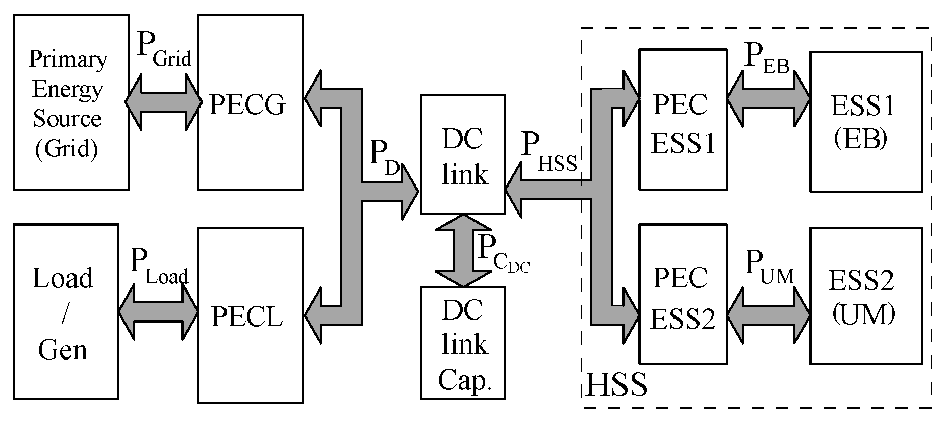
Figure 1 depicts the power flow balance in a generic HSS. The primary energy source (in this case, it is the grid) supplies a given amount of power,
, to the front grid PEC (PECG). The aim of the system is to supply a power flow,
towards another port that behaves either as a load or as a generator, for instance in the case of regenerative breaking applications. This port is interfaced through a Load/Generator PEC (PECL). At every instant, the difference between the load and grid power values,
, is managed by the control at the DC link. An adequate power balance into this DC link is essential for the correct operation of the system. A capacitor bank, DC link Cap in
Figure 1, is usually employed as energy buffer for this difference power, being able to absorb or deliver the required
. In some applications, for instance in islanded operation of microgrids, a very large energy storage capability is required at the DC link. The energy stored in the capacitor bank is normally not enough to ensure a stable operation at the DC link. Therefore, an extra energy storage system is interfaced to this DC link, ensuring also a fast recovery in case large power steps are demanded. Furthermore, in the case of hybrid systems, the total power of the HSS,
, is divided into two different storage units, ESS1 and ESS2, which are interfaced through two power converters, PEC ESS1 and PEC ESS2. The power through the EB and UM,
and
, respectively, is finally interfaced to the DC link.
To ensure a general case, all the power flows in the system must be considered as bidirectional. The conventional control scheme ensures that, upon normal conditions, i.e., power flowing from the grid to the load or from a generator back to the grid, the voltage at the DC link capacitor is kept constant. Then, in the event of sudden fluctuations at either load or line characteristics, the HSS control must compensate the resulting variation of operational parameters to ensure an adequate behavior of the system.
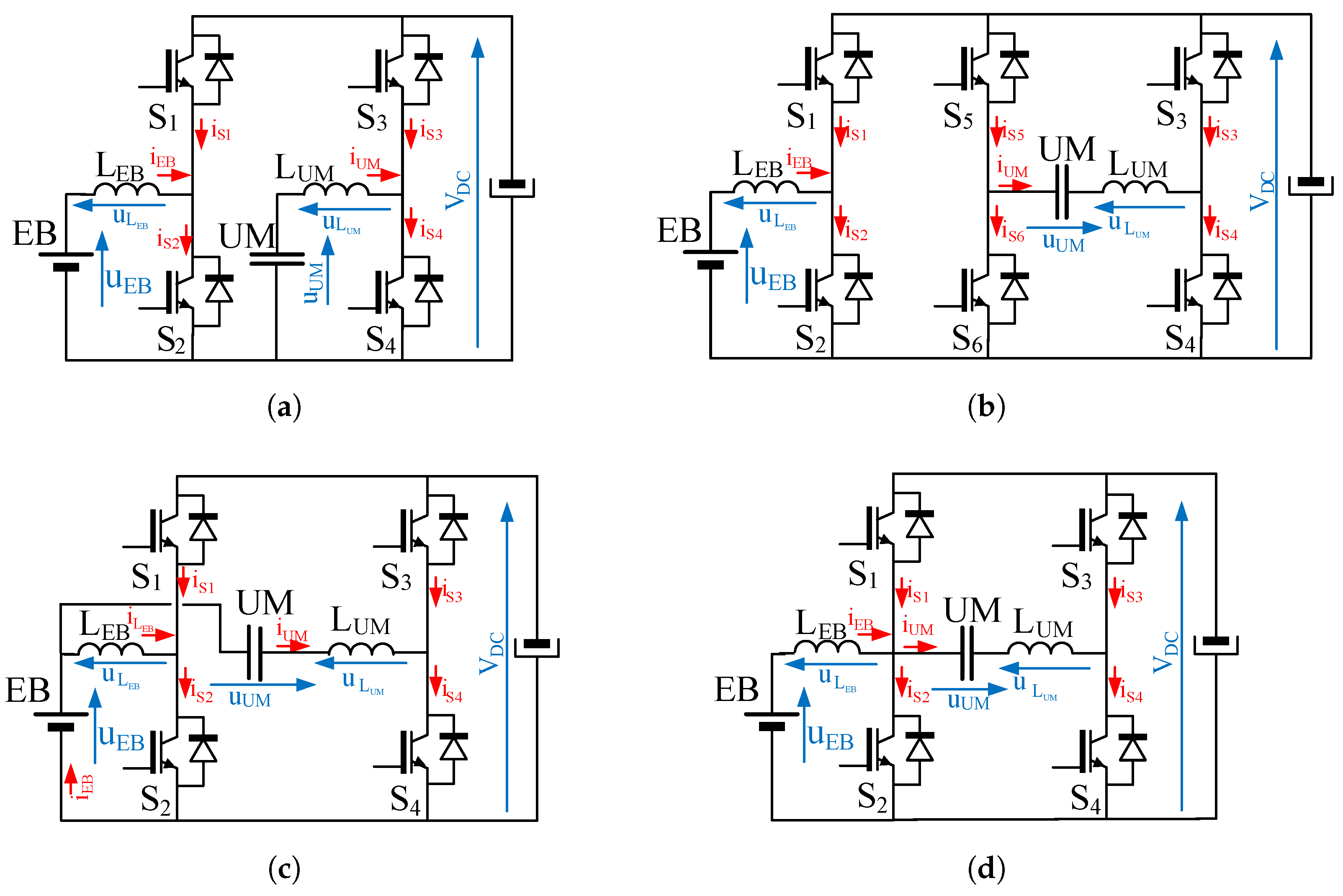
The simplest scheme for a three-port bidirectional converter interface in a HSS, able to attach these devices to a controlled DC link is the Direct Parallel Connection (DPC), can be seen in
Figure 2a [
13,
14]. This scheme is formed by two independent bidirectional boost converters, each of them implemented by adding a filter inductor to a leg of a H-bridge converter. For the sake of clarity, a nominal DC link voltage of 600 V is defined in the coming discussion. In the same manner, the operating voltage ratings for the EB is considered to be in the range of 300–400 V (e.g., a Li-Ion EB intended for grid supporting applications). For these voltage ratios, a bidirectional boost converter can be selected as a feasible solution for interfacing both ports. Nevertheless, considering an extra storage unit with significant lower voltage ratings that requires to be interfaced, the voltage ratios between the DC link voltage and the storage unit voltage will change correspondingly. For instance, in the case of a UM as storage device of, e.g., 48 V voltage rating, and considering a steady-state reference value of 30 V, the direct interface through a boost topology would yield to the operation of the converter at duty ratios around 5%, well beyond the optimal 20–80% range [
15]. On top of major concerns in the effect of parasitic elements, these extreme values for the duty ratio of the converter imply significantly high form factors in the voltage and current switch waveforms at the UM converter leg. In addition, it implies constraints in the practical control margins used in the regulation of the converter. All these issues, which are covered extensively in
Section 2, make mandatory a search for simple, high-gain alternatives to interface low voltage ratings storage devices with the DC link [
16,
17,
18].
The most used alternatives in high power applications include complex cascaded schemes (multistage solutions and tapped-inductor topologies), multilevel converters, or galvanically-isolated converters [
19,
20,
21,
22,
23,
24,
25]. However, for small power levels, these solutions are not cost-competitive depending on the application. To solve these issues, the most straightforward solution in non-isolated converters is to use a Full Bridge Converter (FBC), as depicted in
Figure 2b, for the UM storage system. As is justified in
Section 3, this solution implies higher sizes and costs, as well as increased power losses. After that,
Section 4 explores the non-isolated interfacing scheme proposed in [
16], and depicted in
Figure 2c, based on a Series Connection (SC) of the storage devices. After studying this scheme in detail, its advantages and drawbacks are highlighted. The most important drawback of this proposal is the series connection of both storage systems that eventually makes impossible an independent current control of both storage subsystems. This aspect will be discussed in
Section 4. To overcome the mentioned drawbacks, an alternate solution is finally proposed for high voltage gain applications. The performance of the proposed Series-Parallel Connection (SPC) has been preliminarily explored on isolated applications [
26]. However, this paper is focused on applying the SPC to the non-isolated scheme, as depicted in
Figure 2d, and provides a deeper study than the one carried out in [
27]. Therefore, this work aims to critically assess the performance of the SPC as a non-isolated alternative for HSS applications. This assessment is carried out through a detailed theoretical analysis, which is then validated by means of experimental performance demonstrations on a 10 kW rated laboratory setup.
Section 5 covers the definition and detailed discussion of the switching modes in the converter, whereas
Section 6 provides an analysis of the steady state operation of the topology.
Section 7 evaluates the losses performance of the converter, and compares it to the DPC topology. From the conclusions derived of this study,
Section 8 discusses the operation and suitability of this topology for HSS. A discussion on the control loop implemented for the validation is carried out in
Section 9. Finally,
Section 10 presents the final conclusions on the comparison carried out, and proposes some future work related with this topic.
2. Limitations of the Direct Parallel Connection
As mentioned, the DPC scheme in
Figure 2a is suitable for the interconnection of DC sources when the voltage ratings at the storage systems are in the order of magnitude of half the DC link value. However, when a significantly small voltage ratings storage device is interfaced with a large DC link, i.e., with a ratio of 1:10 or higher, the bidirectional boost configuration is not the optimal option. As a large gain is required, the efficiency and the cost-effectiveness of the design are compromised [
27,
28]. Such a high gain requires a large duty ratio at the lower switch, over 90%. On the other hand, and considering a complementary pulses scheme, the remaining upper switch must be turned on with a very small duty ratio. These extreme duty ratio values yield to low efficiency [
29]. As the switches must be designed for the high DC link voltage, high voltage ratings must be used. However, these devices present relatively large on-resistance values, and therefore conduction losses increase [
30]. Moreover, in IGBT based topologies, this implies large currents at the antiparallel diodes, yielding to operation drawbacks derived from the reverse recovery phenomenon [
31]. Moreover, the high duty cycles limit the switching frequency, as the minimum off-time of the switch must be ensured [
32].
Finally, the dynamic performance of the converter is also affected, since the small duty ratios yield to non-symmetric bandwidths limitation in charge and discharge operation [
27]. This last issue will be evidenced by considering an example of a HSS with the operating parameters of Table 2. In this case study, a 600 V DC link voltage is assumed, with a nominal operation voltages for the EB and the UM of 300 V and 30 V, respectively. All through this work, a particular notation will be used to clarify the discussion. Note that the subscript applied to the parameters for each of the studied topologies include a capital letter to distinguish the different configurations under consideration. In agreement with
Figure 2, the magnitudes related to the DPC have a capital letter
A in the subscript. In the same manner, the subscripts in the FBC include capital letter
B. Letter
C is used for subscripts in the SC, whereas subscripts for the SPC include capital letter
D. For instance, the parameter
(i.e., the duty ratio of Switch S
) is represented as
for the DPC (
Figure 2a), but is notated by
for the FBC (
Figure 2b), and so on.
Initially, the steady state behavior is discussed. Upon these conditions, the corresponding duty ratios for the EB and UM legs are given by:
where
and
are the duty ratios of switches S
and S
, respectively, for the DPC configuration. These relationships come directly from the gains of each leg of the bidirectional topology, which can be defined as:
where
and
are the static gain of the EB and the UM voltages to the DC link voltage, respectively, for the DPC configuration. In this case, the final capital letter
A in the subscript indicates the DPC scheme.
Therefore, it is obvious to see that:
However, these expressions are a function of the topology, and will change for the rest of the topologies considered, as shown in the coming analysis.
2.1. Effects of the Waveform Shape in the Thermal Efforts
The final reliability of the design is a function of the relative value and distribution scheme of the thermal efforts associated to the electrical parameters [
33]. The following paragraph discusses the effect of the shape of the waveforms in the distribution of the electrical stresses of a leg at the converter. Assuming small current ripples, then the form factor (
) of the current waveform for a given switch in the converter follows the general expression for a square waveform:
where
,
and
are the rms, average and peak currents of a periodic square waveform of period
, respectively, being
the interval of the waveform that the current value equals
.
In the DPC topology, for large mismatch between the ratings at the UM and at the DC link, the duty ratio at the UM leg (
) is close to 0%, around 5% in the case under study. This duty ratio at the upper leg can be expressed as:
and therefore:
Analogously for the lower switch:
Therefore, for a duty ratio close to 5%:
This difference between the form factors at the switches of the leg of the UM converter implies that the thermal efforts at both switches are very different. Ideally, to evenly distribute these thermal efforts among the upper and lower switches of a leg, the duty ratios should be around 50%, yielding to
values close to:
2.2. Prototype and Experimental Setup
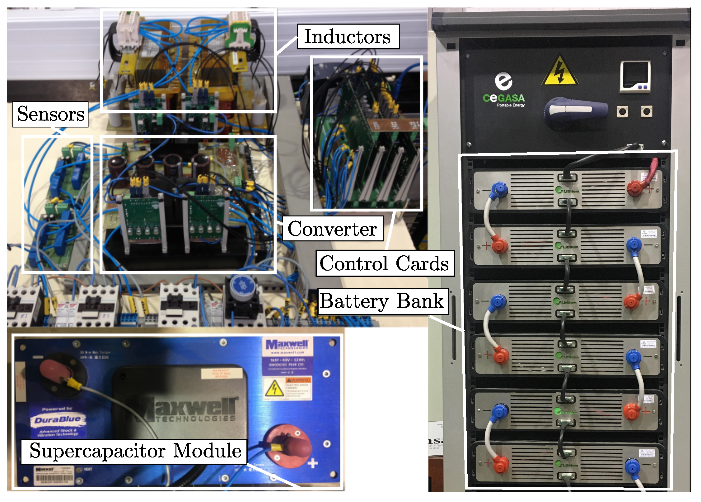
An experimental setup of the PC converter has been implemented in an existing laboratory prototype of 10 kW (
Table 1). The prototype can be configured in all the configurations discussed in this work (
Figure 3). The setup is built using a ROOK 48 × 6 module lithium-ion battery from CEGASA Portable Energy, a BMOD0165 P048 C01 Ultracapacitor Module from Maxwell Technologies and 2MB1200HH-120-50 IGBT modules from Fuji Electric, switching at a frequency of 20 kHz. The setup uses a TMS320F28335 from TI as control platform. The design uses standard reactive elements.
For the conditions of the above description for the DPC scheme, with such a small
, the waveforms of the current through both switches S
and S
in
Figure 2a present average values and
that are significantly different. This issue implies a high mismatch, both in the electrical and in the thermal stresses at each switch.
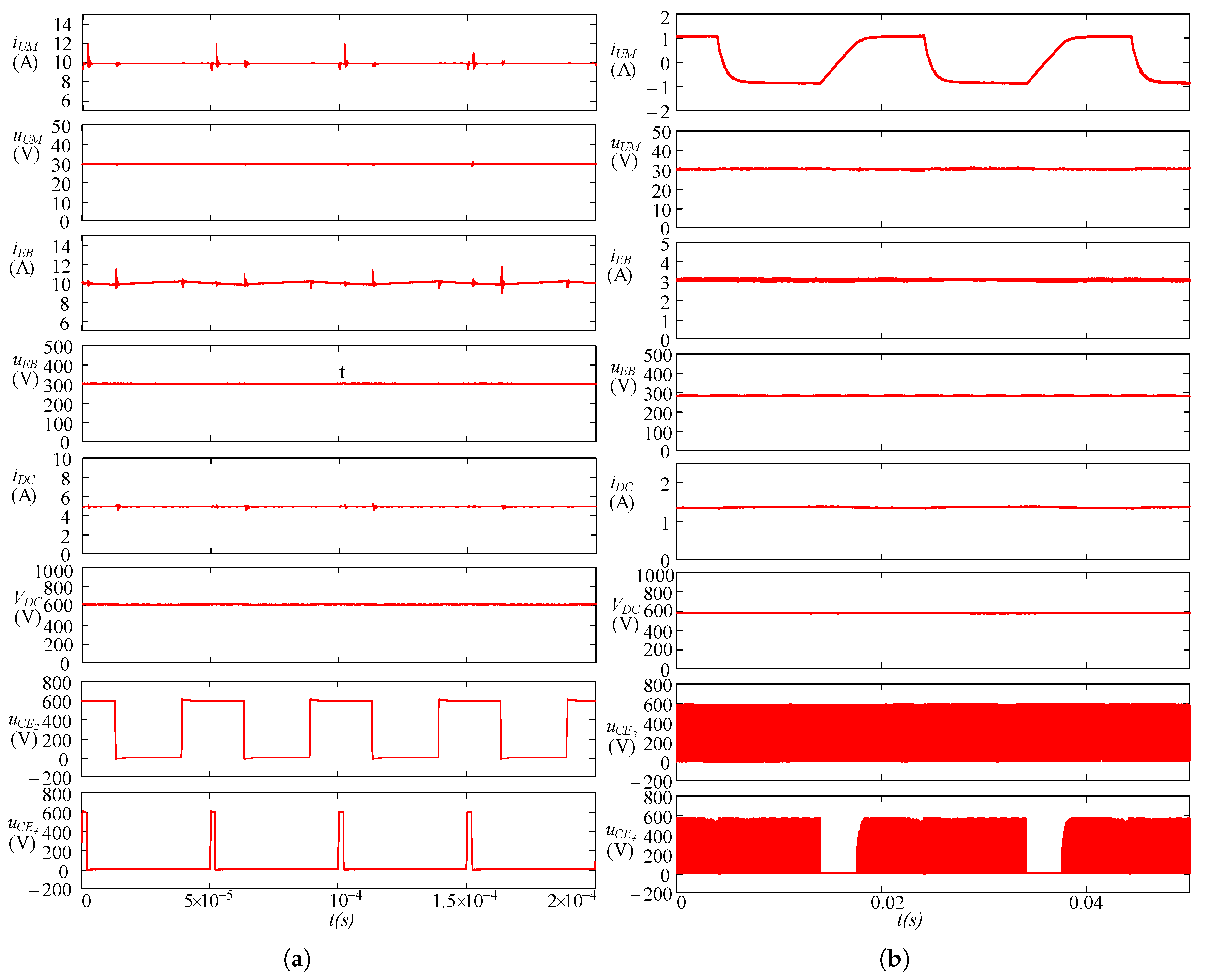
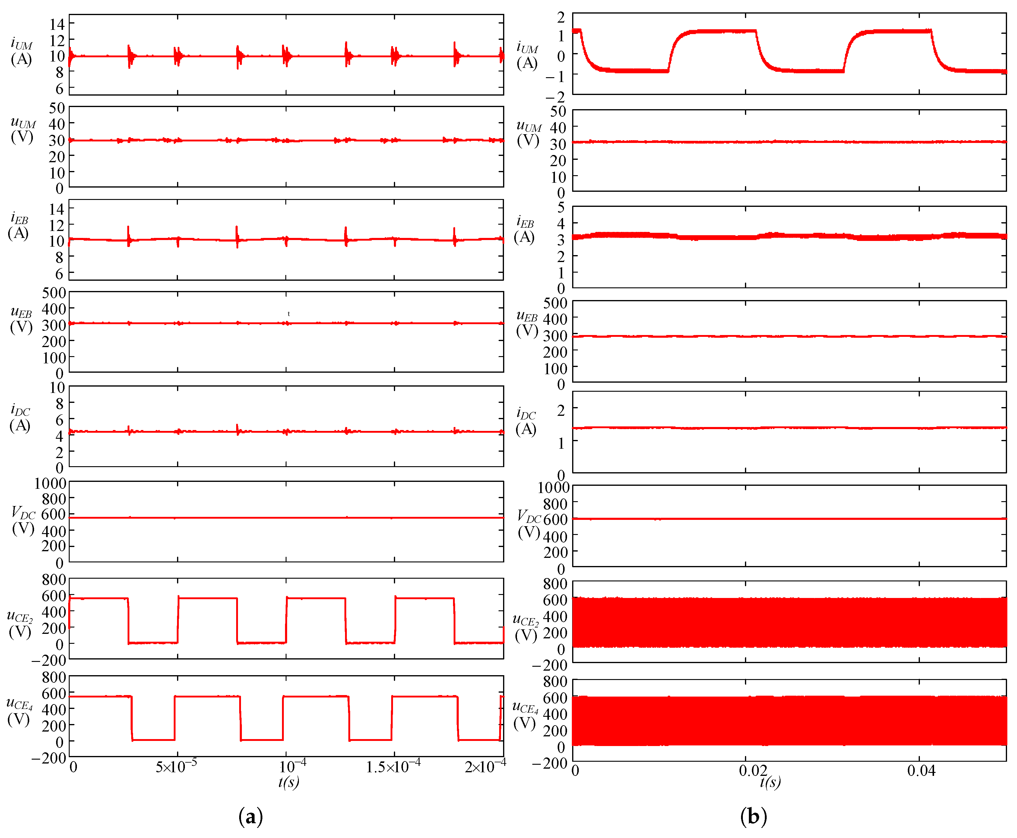
Figure 4a shows these waveforms at the switches, for the setup operating with the parameters in
Table 2. As can be seen, the main currents and voltages measurements, consistent with the references in
Figure 2a, are represented. It can be appreciated how the duty ratio of the switches reach extreme values. This yields to the aforementioned operational and design limitations, that eventually prevent the use of this topology.
As mentioned, the dynamic performance is also significantly affected by the extreme duty ratio values in the UM branch, which are very close to the 0–100% physical limits. Considering an abrupt negative step in the UM current demand, *, then the control stage must generate a control action in the duty ratios that provide the actual UM current, , equal to the reference value. However, the available control actions range from = 5% to = 0%, which ultimately implies S and S continuously turned off and on, respectively. This condition implies that the UM inductance, , is discharged with the relatively small voltage at the UM, , thus implying a limitation in the rate of decrease of the UM current. This aspect penalizes the discharging dynamics enormously, also introducing a non-symmetric behavior in the system performance. Indeed, for the opposite case (charging current), the extreme operation in the control action would imply a charging voltage of , and the rate of charge results dramatically increased.
This situation is illustrated in
Figure 4b, where a series of alternate steps in the UM current reference, from 1 A to −1 A and vice-versa, are provided to the system. Even though these current values are several orders of magnitude smaller than the expected operational range, it can be seen how, at the beginning of the charging step (i.e., current
changing from −1 A to 1 A), the modulation temporarily stops, as
results clamped to 0%. Therefore, the demanded control action would drop to negative values, yielding to an impossible operating constraint. On the other hand, for the discharging step (−1 A to 1 A), the control action can be provided by the system without constraints. Thus, the non-symmetrical performance of the system is demonstrated. Notice that this effect would take place even if the switches are considered ideal.
3. The Full Bridge Converter
To solve these issues, the most straightforward solution among non-isolated topologies is to use a FBC, as depicted in
Figure 2b. During the following discussion, the inductors at the converter are considered ideal and purely inductive, therefore neglecting any parasitic resistances. This simplification is generally accurate for a reasonably good design of the magnetic devices. For the references at this figure, and considering an ideal inductor, the static gain of the UM leg of the converter can be defined as:
where
and
are the duty ratios of switches S
and S
, respectively, for the FBC solution.
As can be seen, the effective gain between the UM and the DC link is the difference between the duty ratios of both legs of the H bridge converter. The value of the duty ratio of the UM branch can be calculated then as:
It is assumed that the duty ratios of S
and S
are complementary to the ones at S
and S
, respectively, as in the following scheme:
In this case, the effective static gain of the UM leg,
, is a subtraction of both converter legs duty ratio levels. In other words, the voltage constraints impose the difference in the values of
and
, but the value itself can be selected arbitrarily. This implies that these duty ratios can reach more adequate values than in the boost converter case, while the difference can be made very small to achieve a large resulting gain. In fact, this effect comes as there is a new degree of freedom that can be selected to have one of the duty ratios, e.g.,
, fixed and equal to 50%. This ensures effective duty ratios at each leg out away from the extreme values, i.e., within the 20–80% areas, therefore achieving better general performance [
27,
28,
30,
31,
32]. In addition, the dynamic range is greater, given that the asymmetric modulation constraint of the DPC solution is not present any more. The payback in this case is the use of two additional switches in a second leg. This issue increases the size and weight of the converter, as well as the switching and conduction losses. However, with this solution the dynamics are not limited to the low duty ratios in the converter [
27]. However, all four switches need to cope with the large voltages at the DC-link,
, even though the device to interface presents significantly small ratings, yielding again to large conduction and switching losses [
30,
31]. A set of experiments has been carried out, configuring the same converter used in
Figure 4 as a FBC. The system operates at a DC link voltage of 600 V, a UM voltage of 30 V, and different current values combinations flowing through both the EB and the UM.
Table 3 shows experimental values of the losses and efficiency measurements of both DPC and FBC configurations, for the aforementioned voltage and current conditions, considering an extended set of UM current values (it must be noticed that the asterisks at any variable represent the references for the control systems). As can be seen, compared to the DPC operation, the FBC losses result increased, and therefore the efficiency of the FBC configuration is significantly smaller.
4. Series Connection of the Storage Systems
Figure 2c shows the series configuration of the storage systems [
10]. It must be noticed how the UM is connected in series to the EB. The analysis of the topology starts by looking at the mesh equation that relates the voltages at the switches S
and S
, at both inductors and at the UM, with the references in
Figure 2c:
where
(
t) and
(
t) are the collector to emitter voltages of switches S
and S
, respectively, and
(
t) and
(
t) are the voltages at the inductors
and
, in the EB and UM legs, respectively. The average inductor voltages will be null at steady state, and thus Equation (
21) can be expressed as:
Given that each leg of the H-bridge operates as a bidirectional boost converter, the average values of
(
t) and
(
t) are again a function of the duty ratios at the upper switches of the H-bridge converter,
, for S
at the EB leg, and
, for S
at the UM leg, respectively. The expressions for the static gain in SC is analog to the ones derived in Equations (
3) and (4), for FBC, but for consistency, they are expressed for this topology as:
Equations (
23) and (24) yield to the expression for the duty ratios,
and
, and the static gains,
and
, in steady state:
From Equations (
25) and (26), the expression that relates the duty ratio from both legs can be calculated as:
Equation (
27) is interesting, since the duty ratio of switch S
at the UM leg, i.e.,
, is not a function of the UM and DC voltage values alone (which would yield to very small duty ratio values as in the DPC), but also a function of the battery voltage. This is has a similar effect to what was found for the FBC scheme. From Equation (
27), for the operating conditions in
Table 2, the duty ratio values at the UM leg of the converter for the DPC change from
= 5% for the DPC to
= 55% in the SC. Therefore, again, the resulting duty ratios at the SC scheme imply a significant improvement in the current stresses balancing versus the DPC case. In addition, the control margins for the control actions achievable in this topology result increased, and in principle this would allow for a symmetrical fast dynamics performance design, in line with the FBC case. The only constraint in the design for SPC scheme is that the voltage at the battery as well as the voltage at the UM cannot reach the DC link voltage. This means the duty ratio of the switch S
at the UM leg must be less than or equal 100% (
). However, for practical values, a feasible system ensuring this condition can be designed without major issues.
However, the most significant drawback in this scheme comes from the expression of the battery current, which can be expressed by:
where
,
and
are the currents of the EB, inductor
and UM, respectively.
This results in the impossibility of implementing a practical decoupled current control scheme in both storage systems (EB and UM). In fact, if both inductor currents are independently controlled, then the evolution of the battery inductor current is forced by Equation (
28), yielding either to dangerous voltages in the system due the inductive behaviour, or to a limited dynamic performance if these overvoltages are prevented at control level.
Another point of the analysis comes by looking in
Figure 2c. From the inductors connection scheme, it might seem that a certain beneficial interleaving effect is possible in the EB current,
. Nevertheless, this effect would only be true for small operating conditions ranges, as it depends on the values of the duty ratios and in the synchronization of the pulses in the switches. This enhanced interleaving effect will not occur for all possible conditions, particularly for UM currents much higher than EB currents.
Finally, also derived from Equation (
28), the peak current flowing through the EB inductor is calculated as a function of the UM and EB currents. Thus, inductor
must be designed considering values in the order of magnitude of the UM current, that is, significantly larger than the EB current. This results in a much larger inductor device, which compromises the efficiency, the power density and the cost of the full HSS.
Given all these constraints, the SC scheme is disregarded as a feasible option. Therefore, it will not be included for the validation stages, by simulations or experimental tests.
5. Analysis of the Series-Parallel Connection
All these drawbacks of the SC scheme can be effectively solved by considering the SPC of both storage units. This scheme, shown in
Figure 2d, keeps the H-bridge configuration of the switches. However, in this case, the series assembly formed by the EB and inductor
, is connected between both midpoints of the legs. This configuration can be seen as an integration of the FBC from three to two legs, removing the degree of freedom that existed in the latter. For the references in
Figure 2d, the mesh equation that includes the voltage at the UM can be expressed as:
Analyzing Equation (
29) analogously to the former FBC and SC cases, the expression for the duty ratio at the UM leg, results in:
Again, it presents a similar expression to the SC case; thus, all statements concluded for the new duty ratio values are still valid.
Regarding the stresses distribution, the values of the
can be calculated for the switches at the SM branch at the SPC configuration, considering the values of
Table 2:
These values are close to the optimal value for an even distribution of the current efforts stated in Equation (
16), therefore increasing the reliability of the system. This effect is obtained for any application in which one of the legs at the converter interfaces a device with voltage ratings significantly smaller than the other one, this latter being around half (e.g., practical values of 40–60%) the DC link value.
However, in addition to that, it must be noticed how, in the SPC scheme, the following expression can be calculated for the EM current:
Therefore, and unlike in the SC case, decoupling both EB and UM current control is quite simple in the SPC scheme. This results in the possibility of implementing an independent current control (and hence power flow) for both storage devices. This allows for an effective hybridization of the energy devices, without the drawbacks of extreme duty rations in the system.
The following discussion deals with a deep analysis of the operation of the SPC converter, aiming to provide the foundations for an adequate design of the HSS. The previous step of the analysis is to settle the assumptions and limitations that are going to be considered to simplify and establish the limits of the study. These assumptions are the following:
The UM is a unipolar DC device, and the terminal of negative polarity is attached to the center point of the battery leg. Thus, it can be deduced from (
30) that
is greater than
in steady state.
The switching pulses of all the switches are synchronized at the same frequency, .
The ripple values of the current through both inductors and of the voltage at the capacitor, are relatively smaller than the respective average values.
Each leg at the converter operates in a complementary scheme, i.e., the pulse signals for the lower switches are the logical inverted pulses of the upper ones. It is also assumed that a dead time is implemented in the switching scheme, aiming to avoid cross-conduction, and that its effect in the overall performance can be neglected.
The initial conditions assume a positive value for , i.e., the battery is being discharged towards the DC link.
Finally, it is also considered a positive value for , i.e., the UM is also being discharged. However, to increase the generality of the analysis, in a later stage, the case of negative will also be considered.
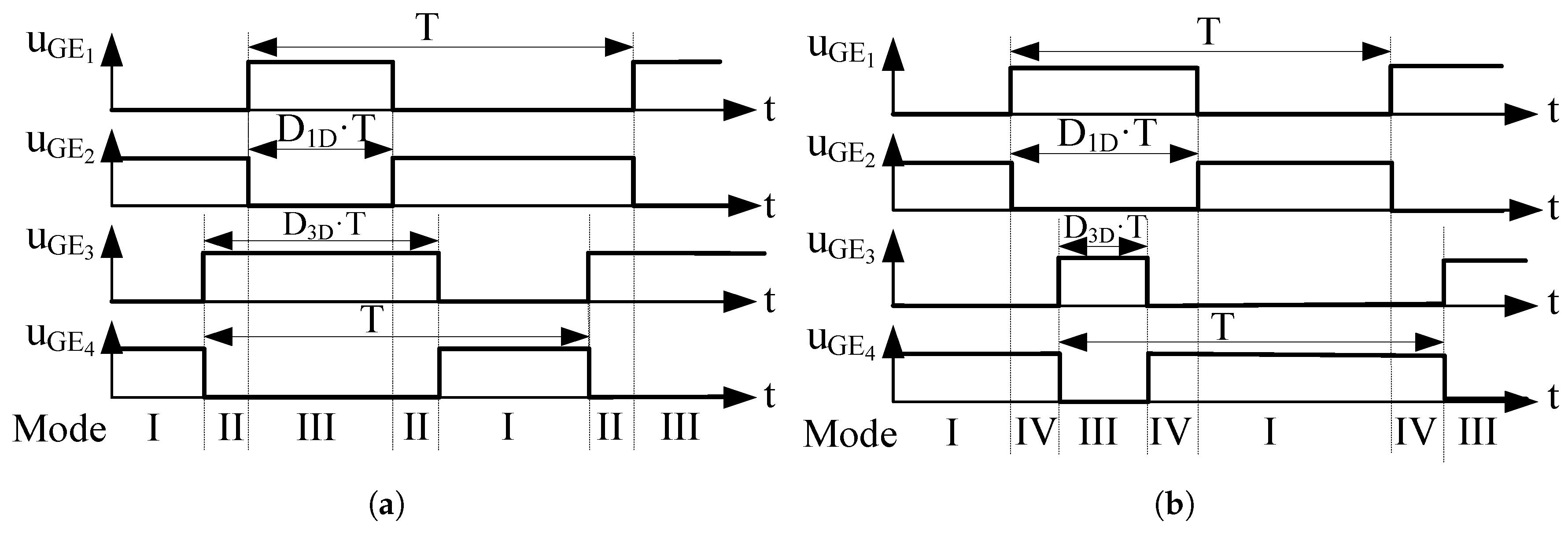
Once the basic operating assumptions are settled, the instant waveforms at the converter must be analyzed. However, the shapes of these waveforms depend on the exact sequence of gating signals in the switches. Each leg operates in complementary mode, as stated previously; however, in the most general case, the phase shift between legs might take any value, resulting in different synchronization schemes. From the point of view of the implementation of the PWM scheme in a digital controller, the most straightforward manner to synchronize the pulses is to use a single triangular waveform at
, and compare this triangular shape with given reference values to generate the control pulses for every switch in the converter. For this single triangular waveform scheme, the pulses obtained are symmetrical from the central point of the on/off intervals, as depicted in
Figure 5. In particular,
Figure 5a corresponds to the switching pattern in the steady state, i.e., for
being greater than
. This gives rise to a set of operating modes, as a function of the combination of on/off states of the switches in the converter. These equivalent switching modes are detailed in the following subsections, considering the chronograms in
Figure 5.
5.1. Mode I. S2 and S4 Turned On
Figure 6a shows both S
and S
turned on. The battery inductor charges through S
(
i > 0). Assuming also
> 0, then
charges through S
and S
:
5.2. Mode II. S2 and S3 Turned On
In the next switching interval, depicted in
Figure 6b, S
turns off and S
turns on, whereas the battery leg remains unchanged. The UM current flows towards the DC link through S
, and therefore:
5.3. Mode III. S1 and S3 Turned On
Finally, mode III keeps the UM leg as in Mode II, but now S
is turned on as S
turns off (
Figure 6c). The resulting current expressions in the switches for this interval are:
5.4. Mode IV. S1 and S4 Turned On
An additional switching mode has to be analyzed. During transients,
might get smaller than
, and therefore Mode IV would take place instead of Mode II (see
Figure 6b) in the switching sequence. In this case, S
and S
will be turned on, whereas S
and S
will remain turned off (
Figure 6d):
6. SPC Steady State Analysis
Once the switching states are defined, the steady state analysis of the SPC scheme can be carried out. It must be noticed that both converters are bidirectional in current, and thus, if a general analysis is desired, all possible combinations must be assessed. Considering a system that operates with DC link voltage control, and provided that both storage device legs are controlled in current mode, the operating conditions that need to be taken into account are stated in
Table 4.
From Equations (
34)–(
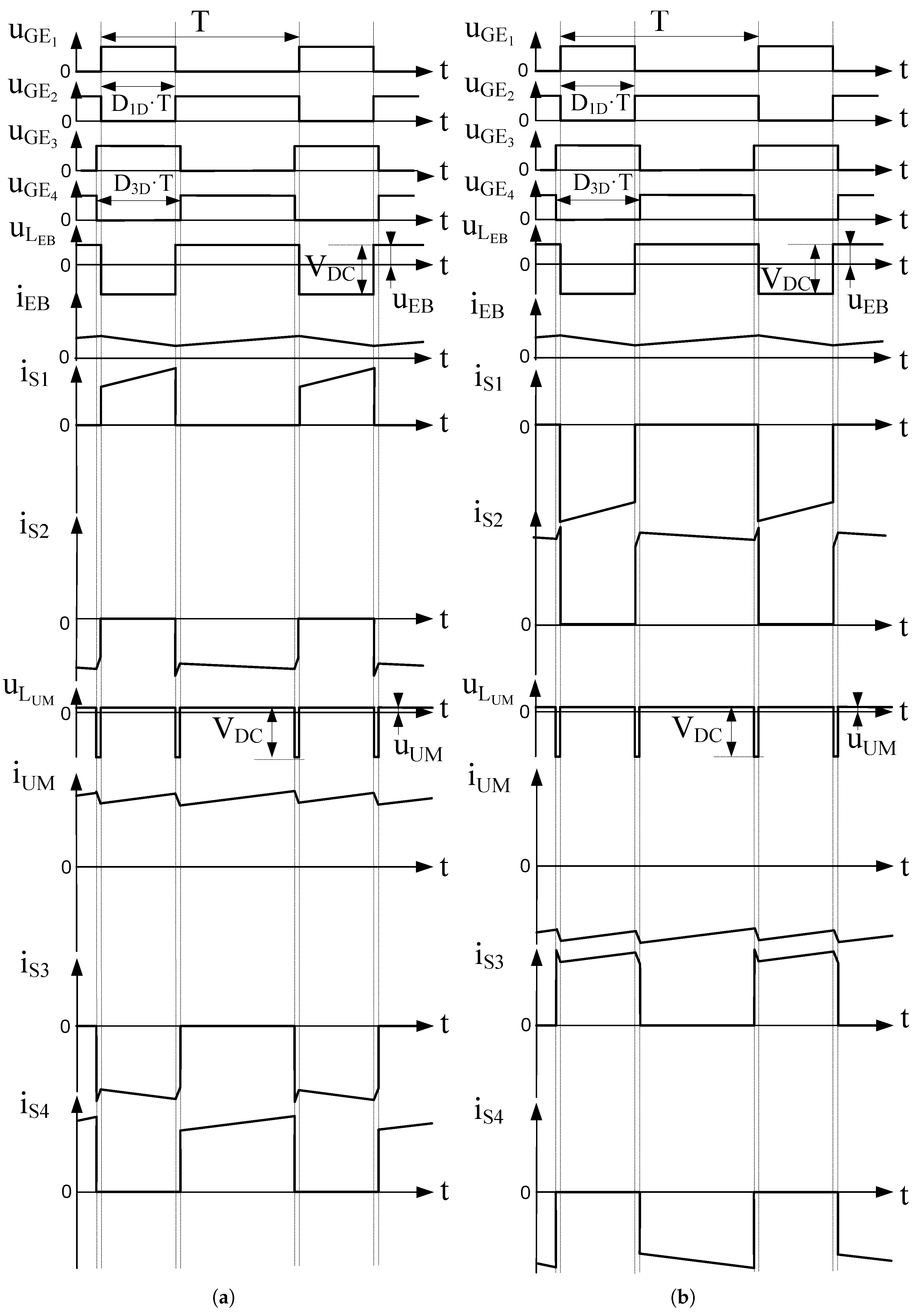
37), the current that flows through the switches at the battery leg are a subtraction of the EB and UM inductor currents. Therefore, the net result of these switch currents depends on whether these currents are added or subtracted in absolute value. Thus, this study can be simplified to the cases in which UM and EB currents have either the same or opposite signs. The theoretical waveforms for these two key cases can be seen in
Figure 7a (EB and UM discharging,
and
have same signs) and
Figure 7b (EB discharging, UM charging,
and
present opposite signs). Even if the resulting current values at the switches result in significant change, the claimed balancing effect in the current stresses at the UM leg switches can still be noticed, as all the involved duty ratios are relatively close to the 50% optimal value.
Another consequence of this switching pattern is that the current waveforms through the UM inductor evolves at twice the switching frequency. This allows for a certain degree of optimization in the inductor design, as current ripple will decrease for the same target inductor value, or, conversely, inductor can be made smaller for the same target current ripple.
Figure 8a shows key experimental waveforms measured at steady state, for the SPC configuration of the prototype setup defined in
Table 2.
However, the most significant consequence of this connection comes from the relationship between
and
, and therefore between
and
. As stated in the assumptions, and considering the steady state operation, then from Equation (
30),
is always greater than
. However, in transient operation, the inductor voltage at the UM might be substantially large, depending on the transient current demanded. This might yield
to reach values smaller than
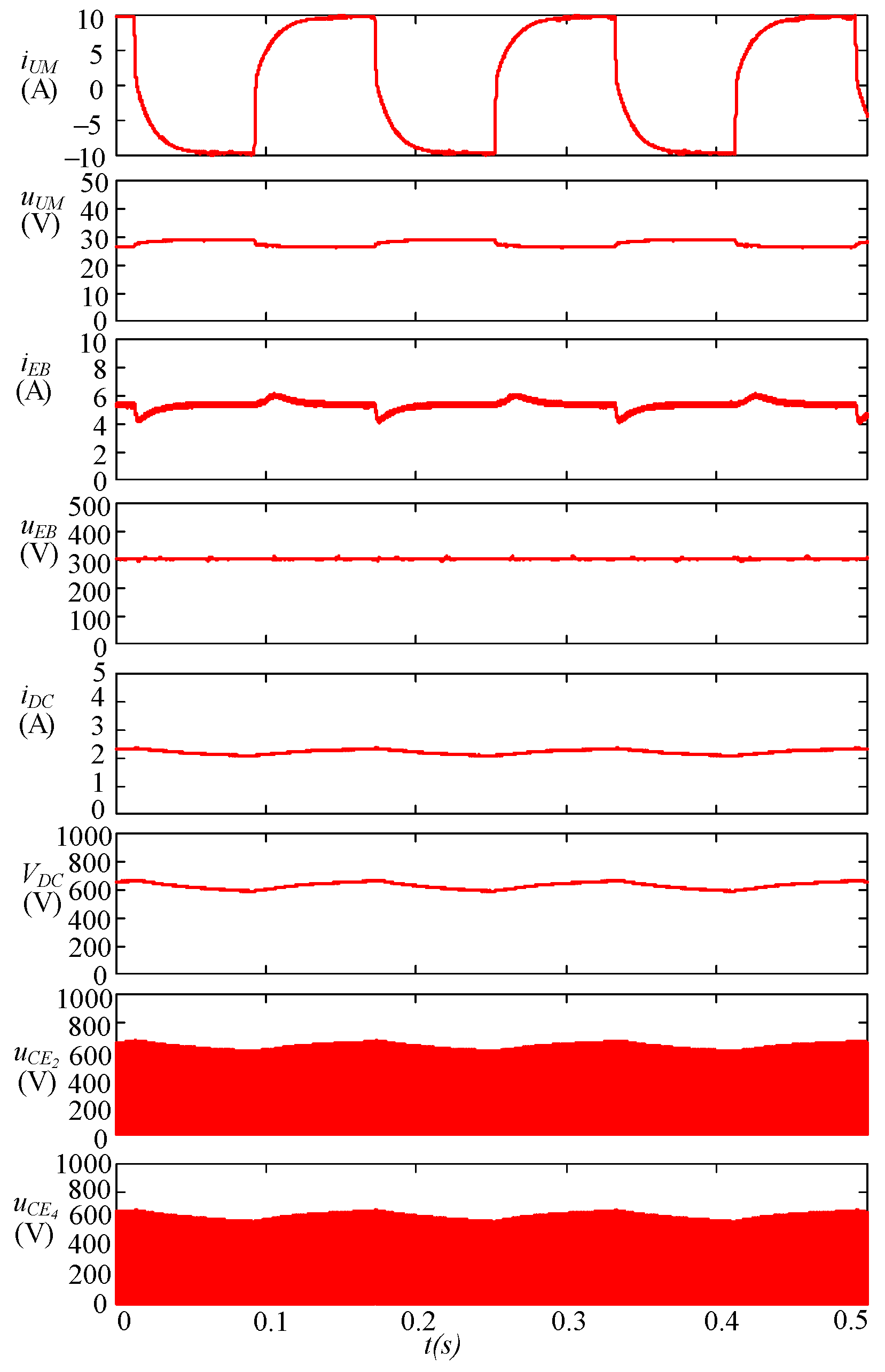
. However, as in the FBC case, now the control action at the UM is not clamped as in DPC, and therefore a better dynamic performance is found. Moreover, this behavior is now symmetric. To illustrate this last assertion,
Figure 8b shows a series of symmetric ±1 A consecutive bidirectional current steps for the SPC connection, in order to keep the same values as in the DPC case (
Figure 4b), as to be compared directly. As it can be seen, and given that the control action is able to reach negative values in a natural manner, the modulation is never interrupted in the SPC operation.
Figure 9 shows the performance for an increased current steps than in
Figure 8b, up to ±10 A current steps. As it can be seen in this figure, a large ripple an be appreciated in the DC link voltage. This is due the fact that for these experiments, the DC link is not regulated with optimal bandwidth. However, the aim of these plots is to show how this topology can supply large, fast current steps to the DC link voltage by the UM storage subsystem.
7. Losses Comparison and Effects in the Efficiency
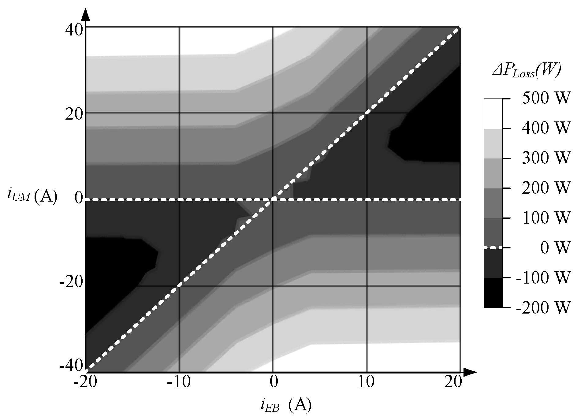
From the above discussion, the SPC can be initially considered as an alternative solution for a non-isolated interface in a HSS, in the case that one of the storage devices is rated at very low voltage. As can be seen, the proposed scheme overcomes the main drawbacks of the DPC, FBC and SC schemes. However, major concerns in the performance of the solution arise from the fact that the UM current will flow also through the switches of the EB leg. It means that both switching and conduction losses through these switches will be affected. In the event that the final losses at these switches result in an increase with respect to the original scheme, the overall efficiency loss might make unfeasible the use of this solution. Moreover, as is demonstrated below, the final balance depends on the operation point of the HSS. Thus, a thorough, objective analysis of the time evolution of losses in the system as a function on the mode of operation must be carried out.
To assess this comparison quantitatively, the losses at every switch of converter have been expressed following a simplified theoretical approach. The generic equations of both the switching and conduction losses, for inductive switching of the converter, have been expressed as a function of the EB and UM current values [
15]. However, to extract conclusions on the comparison of performances, the figure of merit that is considered is the difference between the losses at both the DPC and SPC configurations,
, rather than the losses at each of the schemes on their own. Thus:
This parameter has been quantified theoretically for the operating parameters in
Table 2, and the results are shown in
Figure 10. This picture represents
in a grey scale. The darker areas correspond to larger negative differences, i.e., the proposed SPC performs with fewer losses than the original DPC. Conversely, the clearer regions imply larger positive differences, i.e., SPC performs with more losses than DPC. As a conclusion, a better efficiency is obtained by using the proposed SPC scheme if the system evolves within at the darker areas. This implies both UM and EB currents are large in amplitude and of the same sign, that is to say, both storage devices are simultaneously being either charged or discharged.
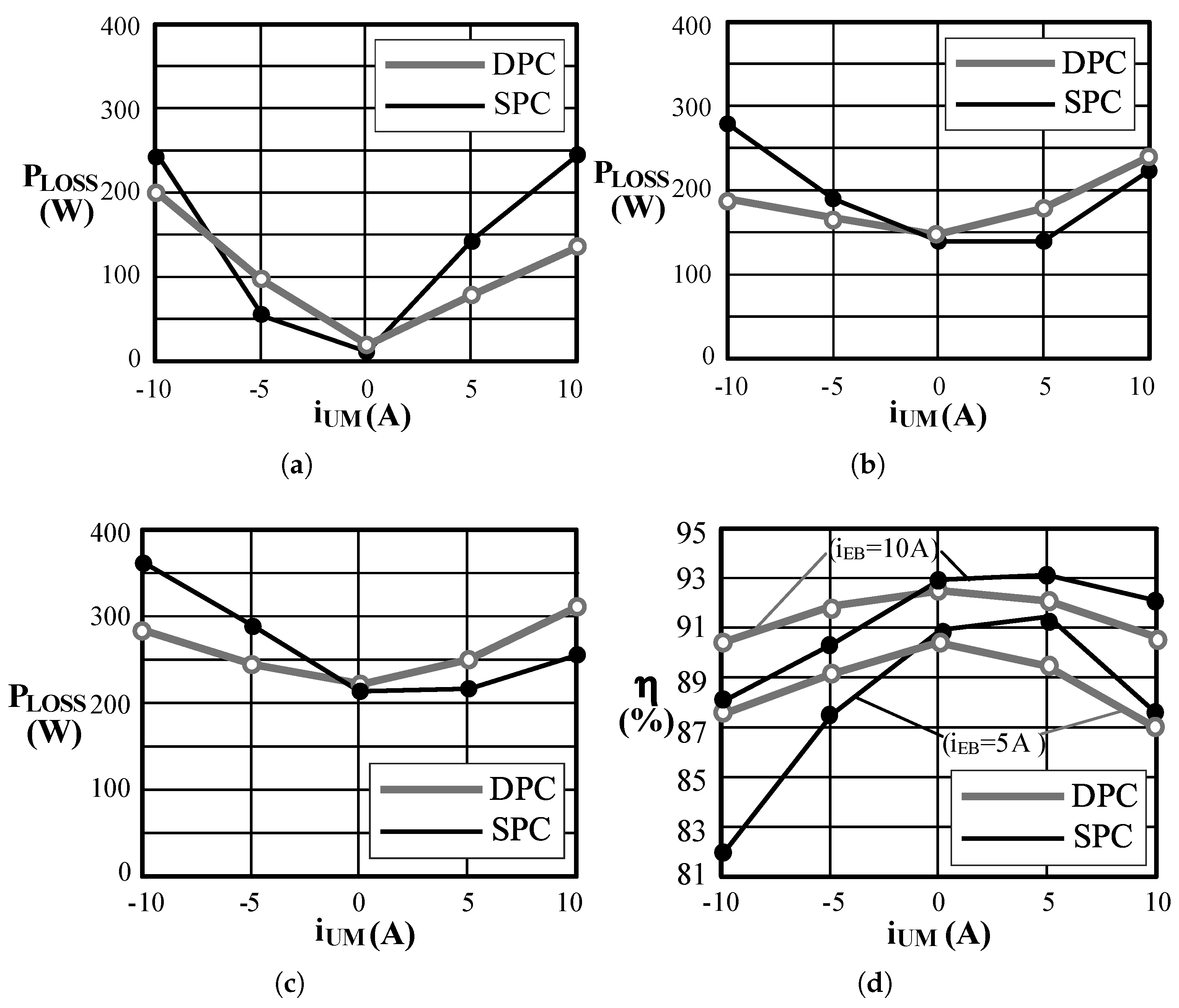
The conclusions of this analysis have been validated through a series of experiments on the built setup.
Table 5 shows efficiencies and losses obtained in steady state, of both the DPC and SPC configurations, for the known given voltage conditions of
= 600 V,
= 300 V and
= 30 V. The recorded current reference values considered were
= −10 A, −5 A, 0 A, +5 A and +10 A, and
= 0 A, +5 A, +10 A. From these results, it can be verified that the switches losses are lower in SPC provided that the UM and EB currents are both large and of the same sign. On the other hand, if the signs of both currents are opposite, SPC presents more losses than DPC. Thus,
Table 5 corroborate the theoretical results depicted in
Figure 10. The results in
Table 5 are graphically represented in
Figure 11. As can be seen, the SPC presents fewer losses when the EB and UM currents have the same sign and larger values. As a conclusion, it must be noticed that, even though at some operating points the losses will be higher with the proposed SPC scheme than in the original DPC scheme, the full performance in terms of efficiency of the proposed topology must be assessed only after considering the application and the control scheme used.
8. SPC Scheme in Hybrid Storage Systems Applications
Thus far, the comparison of losses has been carried out considering steady state conditions. This section, instead, deals with the analysis of the SPC performance in HSS applications upon transient operation. For the power flows stated in
Figure 1:
where
is the power absorbed by the DC link capacitor,
is the power coming from the grid,
is the power consumed by the load, and
and
are the power flowing from both the EB and UM, respectively, towards the DC link. These power values are defined as a function of the voltage and current values at each subsystem [
14]:
where
,
,
,
and
are the currents of the grid, the load, the EB, the UM and the DC link capacitor, respectively, all of them at the DC link side. In the system under consideration, the DC link voltage is regulated and fixed to a reference value. Therefore, in steady state
is null. Assuming that all the load power is supplied by the grid converter, then the storage system remains idle in steady state, which means that also
and
are null. Thus, from Equation (
39), the following equality applies in steady state:
However, upon transient variations modeled by power steps in either the grid (line fluctuations) or in the load (random load/stochastic generator), the balance given by Equation (
47) is lost. It yields to a transient change in the DC link steady voltage value, that must be compensated by the control scheme if a stable operation is desired [
34]. For simplicity, it is assumed that, once the system is in steady state, a load instant power step takes place at a given moment (i.e., the grid power is kept constant). It is also assumed that the hybrid behavior is designed as to achieve UM dynamics (power support) much faster than the EB dynamics (energy support) [
35].
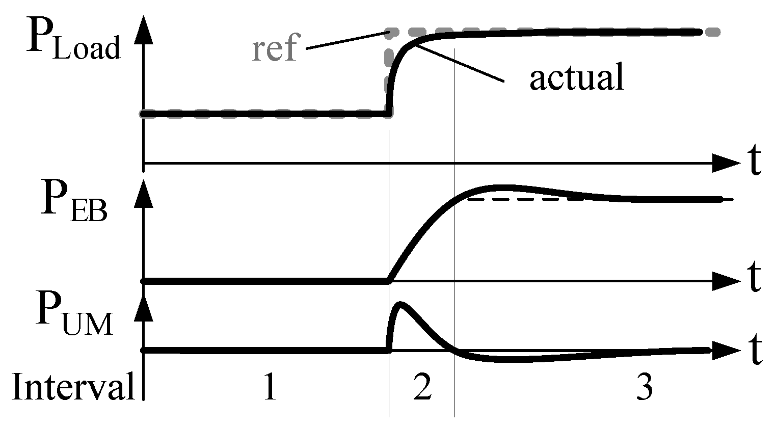
Figure 12 sketches this evolution. Interval 1 shows the initial steady state situation, when no power is flowing from any of the storage systems to the DC link. The power that the load is consuming is fully delivered by the grid. The storage system is in idle mode, and thus the currents flowing through the storage devices are null. Interval 2 starts with a sudden load change, in this case a step increase in the load. The control stage reacts demanding more power from the HSS. Therefore, both storage devices start to supply energy to the system. Due the system constraints, the battery has limited safe dynamic response, and hence the power is initially supplied by the UM converter. In any case,
and
, and therefore
and
, present the same polarity. As per the aforementioned discussion, this results in smaller current stresses in the switches at the EB leg. Notice that an analogous situation is achieved in the case of decreasing step in the load power.
Once the energy supply is taken over by the EB, the UM must recharge to reach the initial reference value again in a reasonable amount of time. This ensures the HSS is ready to supply again any forthcoming power steps. However, this implies that the sign of the UM current changes, yielding to Interval 3. In this situation, EB and UM currents present opposite signs, resulting in an increase of the stresses at the switches of the EB leg. Nevertheless, this evolution back to idle mode might be done relatively slowly, allowing to minimize the effect of the addition of currents. Then, provided that the control dynamics are tuned adequately, SPC provides a better efficient performance than DPC.
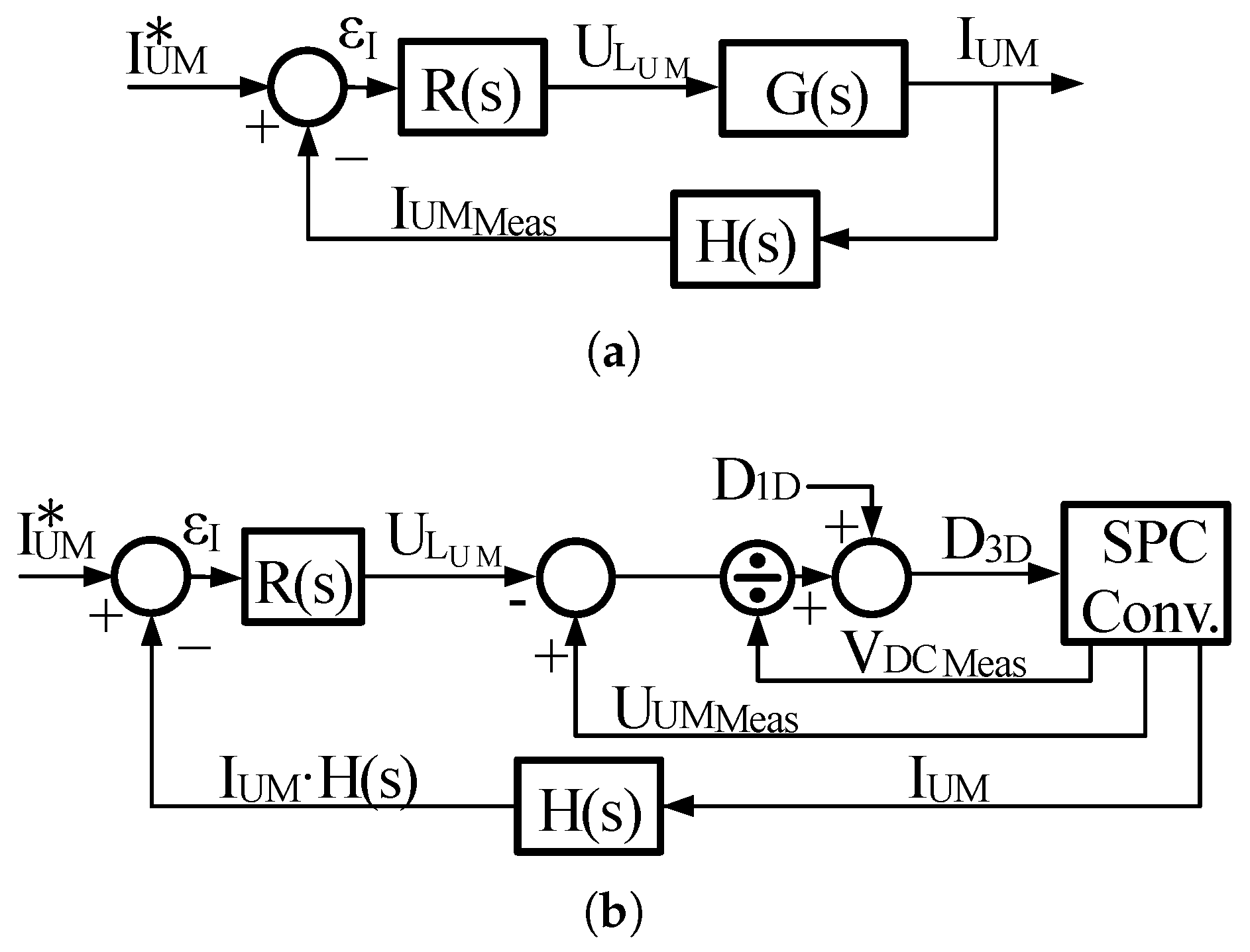
9. Stability of the SPC Scheme
Figure 13a shows the scheme of the UM current mode control loop. Although the standard EB current mode and DC link voltage mode control schemes are not represented, it is assumed that these loops are operating properly.
is a signal conditioning block, in charge of measuring, adapting and filtering the current through the UM. The obtained measured value,
, is compared to the reference,
*, to obtain the UM current error,
. This error is the input of the regulator
. The output of this regulator is the control action that enters the transfer function of the system,
. As seen in
Figure 2d, the UM storage device current equals the UM inductor current, and hence the UM control is indeed an inductor current control. Such a control scheme can be implemented considering the inductor voltage,
, as the control action. This yields to a transfer function given by:
where
is the parasitic resistor of the real magnetic component. This approach results in a simple first order transfer function, and therefore the tuning of the controller can be made very easily. After tuning the regulator, the duty ratio at the UM leg of the converter,
, can be obtained from Equation (
29). After linearizing:
Figure 13b shows the block diagram of the control scheme, where the measured DC link and UM voltage values,
and
, respectively, are used to compute
. The implemented filter
is a second order Butterworth filter, on a Sallen–Key configuration, with a cut-off frequency of 3.5 kHz. The chosen bandwidth of the PI regulator
is BW = 300 Hz. The UM inductor has an inductance value of
= 21 mH and a series parasitic resistor of
= 0.48
.
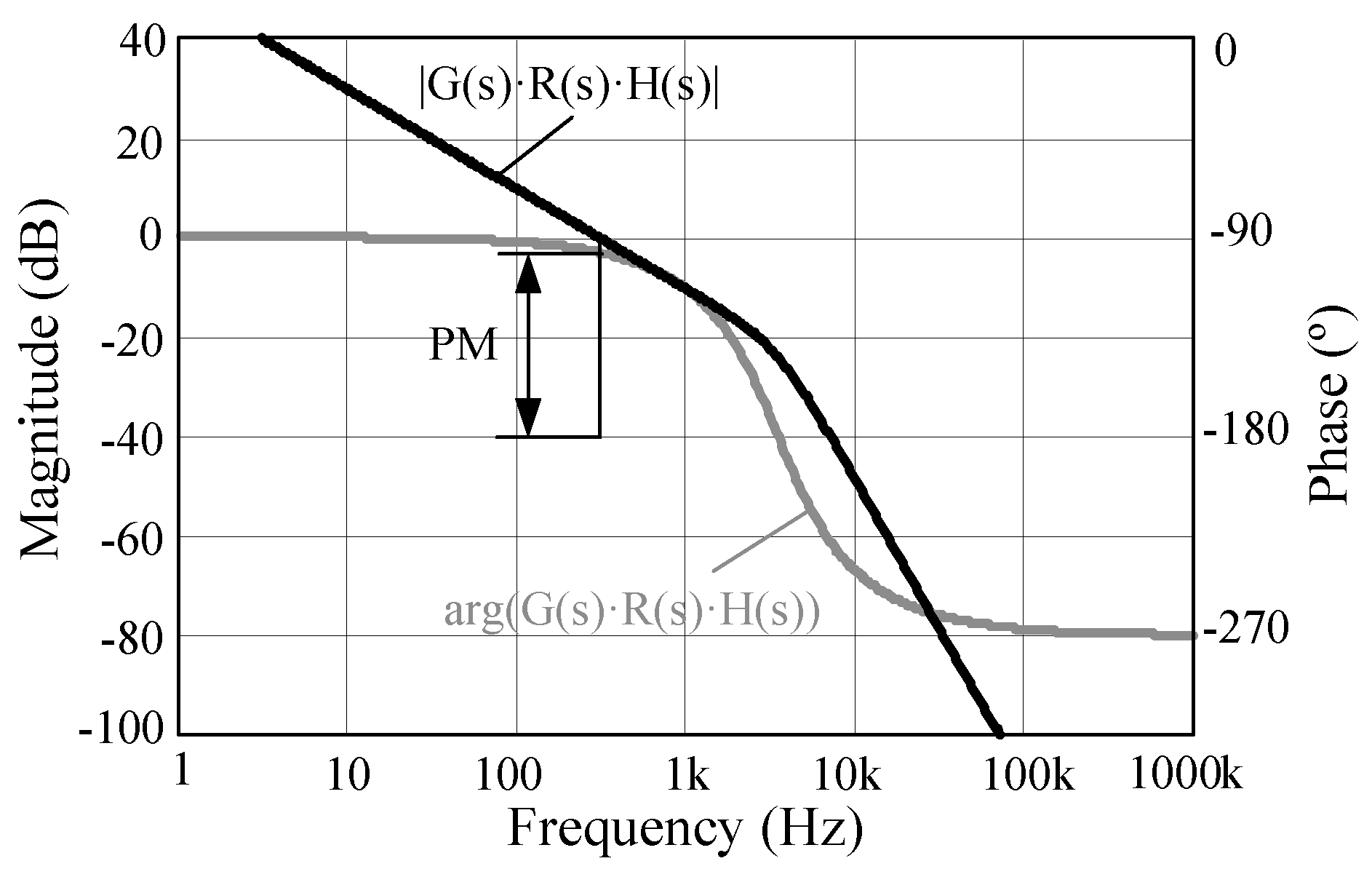
Figure 14 shows the open loop gain of
, used to check the system stability. As can be seen, for this design, the Phase Margin (PM) is close to 90
, therefore the system is stable.
10. Conclusions and Future Developments
In this work, a comparison among basic power converter topologies for multiport Hybrid Storage Systems (HSSs) has been conducted. The conditions in which the results of the analysis are valid have been clearly defined. These particular constraints include the target application HSS, with a DC link interfaced with two storage units, one of them with significantly smaller voltage ratings. In addition, the constraints consider low/medium power levels where galvanic isolation is not a requirement. The control scheme implemented in the analysis manages the storage power flows to compensate the system DC link voltage due load steps or grid perturbations.
The topologies under study are the base Direct Parallel Connection (DPC) of two bidirectional converters, the Full-Bridge Converter (FBC) configuration for the UM leg, the Series Connection (SC) of the storage devices, and the proposed Series-Parallel Connection (SPC) of the storage units. All these options can be implemented by connecting the power switches in the standard single-leg configuration with complementary control pulses switching. This constraint facilitates the final implementation using ready-to-market, cheap components.
The results of the theoretical study, that included aspects such as losses, efficiency, loss balance between switches, and margins in the control stage design, have been validated by means of simulations and experimental tests on a built laboratory prototype with a rated power level of 10 kW. All throughout the analysis, and for the purpose of finding comparable results, the main parameters in the design, i.e., power, voltage and current levels of the devices were kept constant. For the same reason, also the values of the reactive elements were kept constant.
For HSS applications, SPC presents better efficiency (fewer losses) and also a better distribution of the electrical and thermal stresses in the switches of the legs of the converter. The combination of both effects yield to an increase in the reliability of the system.
The conclusions to this study are shown in
Table 6 for DPC, FBC and SPC options. SC has been discarded, as it does not allow the use in HSS due the limitations in the controllability of the storage devices.
From the comparison, it can be seen how SPC presents a better electric and thermal stresses balancing than the DPC case. Given that the UM inductor presents half the inductance value than in the DPC case for the same target current ripple, higher power density might also be achieved. SPC also allows for extended control margin. On the other hand, as mentioned, SC does not allow for an independent current control of the storage devices, therefore preventing its use as hybrid storage solution. For SC and FBC cases, the thermal and stresses balance is similar to the SPC, however FBC presents increased power losses vs. SPC.
The comparative efficiency results show how the performance comparison between DPC and SPC depend on the signs of the currents; therefore, the control scheme determines the overall efficiency of the system. From the above discussion, the proposed SPC scheme is considered as a feasible option for non-isolated interfacing of highly mismatched voltage rating storage systems in multiport configurations, for low to medium power rated HSSs applications.
The key issue demonstrated in this work is that, regardless of the efficiency of the base-case (DPC), an increase in the efficiency, in the dynamic performance, and in the stresses distribution in the converter switches achieved by the SPC connection scheme will be obtained, provided that a set of operating constraints are met. In the performed comparison, the hardware setup has been kept constant, and therefore this gain does not yield to modification in the components count or in the basic control implementation requirements.
Future developments include the optimization of the system for increasing the efficiency and power density assuming SPC scheme as the target topology; the inclusion of the energy storage devices modeling as to refine the control algorithms performance; or extension of the proposed solution in other kind of applications apart from HSS.


