1. Introduction
Digital controllers have conquered new areas where analog control was predominant, such as high-frequency DC/DC converters. Features such as special operation modes [
1,
2], complex control and modulation strategies [
3], self-identification [
4], autotuning [
5,
6,
7], communications [
8], compensator flexibility, and technology integration [
9,
10,
11] are the added values provided by digital control.
Digital control of high-frequency converters has been approached using different control techniques. State feedback techniques have been used in [
12,
13,
14], allowing for the arbitrary placement of the closed loop poles. Full state feedback (inductor current and output voltage) is used in [
12] to implement the control law, providing improved performance in a boost converter acting as a power factor corrector. In [
13,
14], state feedback is applied to multiphase power converters to ensure current-sharing. These techniques are suitable for keeping different quantities in control, typically current and voltage. Therefore, they can be considered as an alternative in multiple loop control structures.
Reference [
15] proposes a time-domain design method. The digital compensator is derived from specified rise time and overshoot. In [
16], the compensator is designed based on the Internal Model Control design method used in motor control. In [
17], complex zero compensation is used to improve transient response. In [
18], the root locus method is applied to the calculation of a digital controller for a multiphase buck converter.
Frequency domain techniques are very popular when designing analog linear compensators for DC/DC converters [
19]. The compensator is calculated by determining the frequency response of the plant and the dynamic requirements regarding their crossover frequency (
) and phase margin (
). A classical design approach, such as the K-factor method [
20] ensures that the magnitude of the open-loop gain is 0 dB at the crossover frequency, and the phase of the open-loop gain provides the required phase margin at that frequency. These design techniques can also be applied to digital linear compensators, considering the discrete nature of the compensator and its implementation, which implies additional factors concerning the analog approach, such as sampling frequency, time delays, and quantization issues. However, the designed controller may not fulfill the expected specifications due to the limitations of the design method itself and the digital implementation—that is, there are
combinations which are impossible to reach.
In [
21], an autotuning system, illustrated with a buck converter, automatically calculated digital PI (proportional-integral), PD (proportional-derivative), and PID (proportional integral derivative) compensators. The
requirements and the knowledge of the converter dynamics issued from the autotuning system were the basis for the compensator calculation, but this design approach does not consider in detail the attainability of
and
PM requirements. In [
22], the digital compensator was calculated directly in the
z domain, taking a given value of
and
as target performance, without a previous analysis of which of their values could be reached with the proposed compensator type. In [
23], the compensator calculation was integrated into the design and optimization process. The design space of the power converter was analyzed considering that the controller was a digital PID, including saturation effects. Different design spaces were proposed, with each one for a particular
specification.
In all the cited cases, the compensator was calculated from the desired values of and the rest of the bandwidth was ignored. Thus, due to the frequency response of the system, the open-loop gain may cross 0 dB at frequencies different to the crossover frequency, yielding a design that does not meet the dynamic specifications and which could even be unstable. Because of this limitation, each design must be checked after its calculations. If the design does not meet the requirements, it is difficult to decide whether to modify the dynamic specifications, change the topology of the compensator, or modify the sensor.
Thus, it is very interesting and useful for the designer to know the limited set of possible achievable dynamic specifications for a combination of a power converter, compensator, and sensor. This set determines the performance space of the controller regarding the achievable crossover frequency, , and phase margin, .
References [
24,
25] present studies of the design space of analog compensators. However, there are issues related to digital implementation that have an impact on the calculation of the design space and require further investigation, such as sampling frequency, time delays, and limit cycling [
26,
27]. The consideration of these effects involves additional boundaries and substantially modifies the aspect of the performance space.
This paper proposes a design tool integrating frequency-based design techniques to: (a) determine all the possible solutions without establishing, a priori, the design target ; (b) assess the influence of different parameters of the compensator on the dynamic performance of the system; (c) determine the simplest compensator design regarding the dynamic performance for a given dynamic specification, the complexity of the implementation and the computational resources.
This work presents the algorithms to calculate this new performance space and analyze their impact on the controller design. The graphical representation of the performance space in the axis can provide the designer with a deep insight on the influence of design parameters through sensitivity analysis. The contribution of this paper regarding prior work is the exhaustive analysis of the digital compensator design (especially in the case of PID); consideration of the limit cycling conditions; and experimental validation.
Section 2 deals with the proposed approach to designing the digital compensator, the description of the limit cycling conditions, and the proposal of a criterion to compare the performance of compensators that provide the same crossover frequency and phase margin. The performance space is introduced in
Section 3, defined as a set of feasible and stable designs characterized by their dynamic performance regarding
.
Section 4 presents the experimental validation of the proposal.
Section 5 summarizes the conclusions of the work.
2. Elements for the Calculation of the Digital Compensator
2.1. Model of the System in the Frequency Domain
There are different approaches to calculating a digital linear compensator to control a power converter. One of them is based on the calculation of a continuous compensator that fulfills the dynamic requirements [
28,
29]. This continuous compensator is discretized by means of conventional methods, such as bilinear or Tustin transformation, to obtain the discrete compensator. This approach provides robustness to the design and confidence for analog designers. However, in some cases, the resulting controller is more complex than required because it includes additional poles that are not necessary for the digital controller (e.g., high-frequency poles are not required since the controlled quantity is sampled at the switching frequency).
A second approach is based on calculating the exact model of the converter in the discrete domain, obtaining its
z transfer function [
30,
31]. This alternative allows for the direct calculation of the discrete compensator using conventional design techniques for discrete control systems. However, this modeling technique is less extended among the conventional design procedures.
The approach used in this work is based on the frequency response of every block, with its continuous or discrete nature being independent and the frequency range limited to half the switching frequency. Although this is an approximation, it works well, as described in later sections, and provides flexibility to the designer. The elements of the block diagram (
Figure 1) are as follows:
The discrete compensator is the element to be calculated. Its frequency response is calculated by the direct substitution of by , where is the sampling period. Despite the sampling period and switching period not necessarily being equal, in this work, they are considered the same for the sake of simplicity ();
Switching power converter
. The more accurate approach to obtaining the frequency response of the power converter (plant) is exact discrete modeling [
30,
31]. However, good results can also be obtained by using averaged modeling techniques [
19,
32] or experimental measurements. If a continuous averaged model is used, the small alias approach should be ensured. In the case of exact discrete modeling or experimental results, the effect of a large ripple is inherently considered;
Time delay
. All time delays are lumped in a single block despite their origin: modulator [
32], analog to digital converter (ADC) and computation. This approximation is valid in most cases. More detailed descriptions could consider the time delay block split in several parts, but this approach is numerically equivalent to the consideration of a single block;
Static gains of modulator () and analog to digital converter ();
Sensor transfer function .
The key transfer function to calculate the compensator is the uncompensated loop transfer function
TU given in Equation (1), where
. The open-loop transfer function
T is defined in Equation (2).
2.2. Compensator Calculation
The calculation of the compensator is based on the specified phase margin and crossover frequency in Equations (3) and (4). Therefore, there are two constraints: the first concerning the definition of the cross-over frequency,
, since the magnitude of the compensated transfer function has to be equal to 1 at
Equation (3); and the second concerning the definition of phase margin,
Equation (4).
Without loss of generality, two different compensator types are considered: PI (5) and PID (6).
As previously explained, the compensator is calculated from the frequency response of the different blocks of the system. The frequency response of the compensator depends on the topology (PI or PID) and can be calculated by Equations (7) or (8).
In the proposed form, the PI regulator has only two parameters ( and ) that can be determined using the constraints (3) and (4). In the case of PI and PID, if the value of issued from calculations is negative or complex, the solution must be discarded since it yields zeros outside the unit circle or complex coefficients in the difference equation, respectively.
However, the PID compensator has three parameters (, and ), while there are only two constraints from dynamic requirements ( and ). Therefore, an additional constraint must be established to calculate the compensator. In this work, two possibilities are considered as an additional constraint to determine the coefficients of a PID compensator:
PID1: the ratio between the frequency of one of the zeros
and the crossover frequency
is given by the designer, as expressed in Equation (9). This approach is a generalization of the proposed calculation criterion given in [
33]. In this case, it is possible to derive an analytical expression of the compensator design parameters
and
as a function of the uncompensated transfer function value at
,
, and
, as depicted in Equations (14)–(16).
PID2: the ratio between the frequency of both zeros is given by the designer, as expressed in Equation (10). When this ratio is equal to one, both zeros are located at the same frequency, and there are analytical expressions to calculate the compensator parameters Equations (17)–(19). However, for other values of
K2, it is not possible to derive analytical expressions to calculate the parameters directly, because the resulting equation is transcendental. Therefore, numerical methods are required to solve the nonlinear resulting expressions.
In the following paragraphs, the equations to calculate each of the proposed compensators are summarized. Thus, the expressions for the calculation of proportional-integral (PI) compensator are Equations (11)–(13). Equation (11) is the transfer function, Equation (12) is the difference equation and Equation (13) is the zero location.
where:
Expressions for the calculation of proportional-integral-derivative PID1 compensator are Equations (14)–(16). The transfer function is Equation (14), the difference equation is Equation (15) and Equation (16) provides the location of zero 1 (note that the frequency of the other zero is determined by the value of
).
where:
Finally, expressions for the calculation of PID2 compensator are Equations (17)–(19). The transfer function if Equation (17), the difference equation is Equation (18). Equation (19) is applicable when both zeros are located at the same frequency (
).
where:
In the case of PID2 compensator with two zeros at different frequency (), a numerical approach is used to find the frequency of the zeroes.
2.3. Analysis of the Calculated Compensators
The expressions (11)–(19) provide the compensator parameters to meet the requirements of gain and phase only at the crossover frequency. However, as mentioned in the introduction, because of the frequency response of the plant, the behavior of the open-loop gain at other frequencies can render the solution unstable or not feasible, or even result in a different dynamic performance than expected. Thus, it is interesting to analyze these possibilities considering the whole bandwidth of the loop transfer function.
Five combinations of crossover frequency and phase margin have been considered to analyze the different possibilities. The resulting linear compensators yield the open-loop gain transfer functions illustrated in
Figure 2. The plant considered in the calculations is a buck converter (input voltage Vin = 12 V, output voltage Vo = 3 V; output inductance L
O = 1 × 10
−6 H; output capacitance C
O = 47 × 10
−6 F; output power Po = 10 W; switching frequency fsw = 1000 × 10
3 Hz; total time delay td = (1/fsw) × 0.5). In the plots, the continuous line represents the theoretical frequency response, while the crosses correspond to the frequency response obtained from time-domain simulations using the discrete compensator performing and ACsweep with the commercial simulator PSIM.
Case 1 (target , target ) is a feasible solution, since the magnitude of the open-loop gain crosses 0 dB only once, the phase crosses −180° only when the magnitude is lower than 0 dB, and the obtained zero frequency is real and positive.
Case 2 (target , target ) is a conditionally stable solution, because the phase is lower than −180° at frequencies where the magnitude of the open-loop gain is higher than 0 dB. The point −1 is outside the Nyquist contour, but a decrease in the gain of the system could make the system unstable. Thus, this solution is discarded despite the resulting system not being formally unstable, and the crossover frequency and phase margin should not be included inside the performance space.
Case 3 (target , target ) is unstable because the phase is lower than −180° when the magnitude is higher than 0 dB. Therefore, this solution must be discarded.
Case 4 (target , target ) is stable, but the effective crossover frequency is lower than expected due to the two crossings through 0 dB that appear approximately at 5 kHz and 15 kHz. The result is that the settling time of the system does not correspond with the target crossover frequency, and the system is slower than expected. Thus, with this design procedure and digital compensator, it is not possible to achieve the specified combination of crossover frequency and phase margin. This combination should be considered out of the performance space.
Case 5 (target , target ) is stable, but the effective crossover frequency is higher than expected. This means that the dynamic response of the system does not match the requirements. Moreover, the effective phase margin is lower. Therefore, this solution is also discarded.
The main conclusion of this analysis is that there are combinations of dynamic specifications that yield designs which should be considered out of the performance space. Reasons to discard the resulting designs are as follows:
The magnitude of the resulting open-loop gain crosses 0 dB more than once: the solution is discarded since the effective phase margin is different than expected. Thus, the resulting design does not fulfill the dynamic specifications;
The phase of the resulting open-loop gain crosses −180° with a magnitude greater than 0 dB: the solution is discarded because it is unstable or conditionally stable.
2.4. Limit Cycling Conditions
One of the characteristics of digitally controlled power converters is the limit cycles that can appear under different conditions. This issue is still a subject of research, especially in the case of transient conditions; but in the literature, different conditions have been established to avoid limit cycling [
26]. Some of them are related to the relative resolution between the PWM (pulse width modulator) and the ADC. These are out of the scope of this work, since they do not depend on the compensator calculation, but rather their hardware implementation. However, there are other two conditions related to the design of the linear compensator.
The first condition [
26,
27] is related to the compensator integral gain
, defined in Equation (20). The expressions of the integral gain
for PI and PID compensators are given in Equations (21) and (22) respectively.
This integral gain
must be limited in order for a single unit impulse of the error signal to produce a step change in the controlled quantity (e.g., output voltage). This condition is expressed in Equation (23). Theoretically, the parameter
is equal to 1, but in practice a, safety factor is considered, which can typically be
.
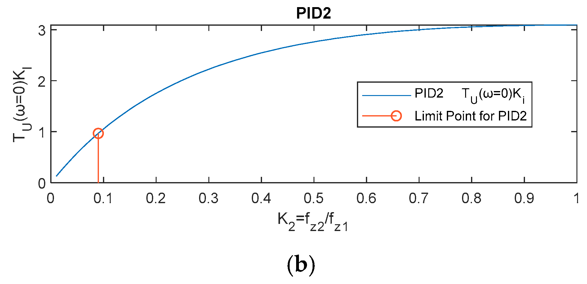
Once the digital compensator is calculated, it is easy to check if it meets Equation (23) to determine whether the solution should be discarded and considered out of the performance space. However, when analyzing Equations (21) and (22), interesting trends can be identified. In a PI compensator, as and are directly determined by the constraints imposed by and , the only possibility to avoid limit cycling is to change ; that is, to modify the dynamic requirements. On the other hand, in the case of a PID compensator (topologies PID1 and PID2), the additional degree of freedom can be used to avoid limit cycling without changing the and requirements, but by changing the parameters of or in Equations (9) and (10).
This effect is illustrated in
Figure 3. The plots show the value of
depending on the parameters
or
and for a given combination of
and
. When
or
are small enough, the plotted product is lower than
, so a limit cycling condition is avoided. The conclusion is that by decreasing the frequency of one of the PID zeros, the gain of the system at low frequency is limited enough to avoid the integral gain limit cycling. However, one zero at low frequency can result in a poor low frequency response, as will be shown in the next section. Therefore, a trade-off must be found.
The second limit cycling condition refers to the requirement of a minimum gain margin,
, to avoid limit cycling due to the sampling effect in Equation (24), where the parameter
is the security margin.
This condition depends essentially on the crossover frequency
. When a high
is desired, close to the Nyquist frequency, the gain margin is limited, since the slope of
is limited for a PID compensator beyond
. Thus, changing the value of the PID parameter has a very slight effect on the
, since beyond
, the value of
is very similar even if there are significant differences for low frequencies, as illustrated in the open-loop gain displayed in
Figure 4a.
2.5. Difference among Solutions with the Same Crossover Frequency and Phase Margin
According to the previous section, for a given and , there is only one possible design if all the parameters are fixed: the type of compensator, sampling frequency, parameters or , and so forth. Following the previously described criteria, it is possible to determine which designs are included in the performance space and which are not. However, it would be interesting to provide a method to compare the different solutions and indicate the best one in terms of the complexity of the implementation, the computational resources, and so forth. Thus, a PI compensator is preferred to a PID for the same crossover frequency and phase margin, since the difference equation has fewer coefficients (expressions (11)–(19)). The compensator with a lower sampling period is preferred, since its implementation needs fewer digital resources.
However, for the PID compensator, there are different possible designs, since an additional design constraint is used either in PID1 and PID2. Therefore, a performance index should be established to choose between compensators with the same architecture and different parameters.
Figure 4 illustrates this issue. Two different PID2 compensators with different values of
have been calculated. Both achieve the same
and
, but their frequency response is different in the rest of the bandwidth (
Figure 4a). The difference in magnitude is approximately 9 dB in the range of 100–1000 Hz for this illustration example. Thus, the transient response for a reference step is also different. When evaluating the error output voltage signal in the time domain—that is, the difference between the output voltage reference (reference signal) and the actual output voltage (measured controlled signal) in
Figure 4b, the design with a lower magnitude in the range of 100–1000 Hz exhibits a longer settling time.
To compare different designs with the same
and
as those appearing in
Figure 4, the performance index
is defined in Equation (25). This index is the norm of the difference between the closed loop transfer function of the system
compared with the ideal one, which is equal to 1 at any frequency;
is the
k-th element of the frequency vector, considering that the proposed design approach is numerical.
is obtained from the open-loop transfer function
. A weighting factor
is included to give more importance to the low frequency response. The factor
is considered to take the non-linear spacing in the frequency vector into account.
The ideal value of this index is
L = 0, which means that the closed-loop transfer function is equal to 1. Comparing two different solutions—that is, two different compensators, the best solution corresponds to the minimum value of index
L. It is difficult to find an exact relationship between the proposed index
L and the conventional time domain indexes. However, in all tested cases, a higher value of
L means a higher error in the time domain, as illustrated in
Figure 5, where six different PID designs for the same
are compared. The parameters changing from one design to a different one are
and
, as defined in Equations (9) and (10) respectively—that is, the separation between zeros of the compensator. Designs A have higher values of
and
than designs B, and both have higher values of
and
than designs C. In
Figure 5a, the frequency response for the different designs is shown. In this particular case, designs PID2B and PID1B are very similar (for example, PID2B is 0.08 dB greater than PID1B at 400 Hz). In
Figure 5b, the RMS (root mean square) value of the error signal in the time domain is plotted for the six designs, considering an output voltage reference step and normalizing the values to the lowest RMS value. In
Figure 5c, the value of the proposed
L index normalizing the value to the lower
L index value is shown. Although there is no linear relationship between the time-domain error RMS value and
L index value, the lower the
L index value, the lower the error RMS value.
Time-response performance indexes are an extended tool to compare compensator performance [
34]. However, since the presented design approach is based on the frequency domain, it is desirable to establish a performance index based on the frequency response to quickly compare different compensator performances. Note that if the design method requires the comparison of many solutions, saving computational resource is important.
3. Determination of the Performance Space
The previous section introduced the frequency-based model of the system, the calculation of different compensator topologies, the criteria to determine whether the designs fulfill the dynamic requirements, and an index to compare compensators that provide the same dynamic specifications .
However, significant advantages can be obtained if the proposed calculation procedure is automated and applied to find a performance space in such a way that all the possible combinations of
that can be fulfilled are found. Thus, the performance space is graphically represented in a plot with frequency units in the horizontal axis and phase units in the vertical axis. In [
25], this plot is called a solution map. In this paper, the design space is the set of parameters of the compensator that have to be calculated to obtain given results regarding
—that is, to obtain a given performance. Those parameters of the compensator are, finally, the coefficients of the difference Equations (12), (15) and (18), and the performance is the pair
. In the following paragraphs, an example illustrates the generation of the performance space
and the influence of different factors, such as the type of compensator and limit cycling conditions. The specifications of the power converter used as our example are as follows: buck topology, input voltage Vin = 12 V, output voltage Vo = 3; output inductance L
O = 1 × 10
−6 H; output capacitance C
O = 47 × 10
−6 F; capacitor equivalent series resistance R
ESRC = 20 × 10
−3 Ω; output power Po = 10 W; switching frequency fsw = 1000 × 10
3 Hz; total time delay td = (1/fsw) × 0.5.
In
Figure 6a, the uncompensated open-loop transfer function
defined in Equation (1) is shown, including time delays, static gains, and the converter-transfer function (
Figure 1). In
Figure 6b, the described performance space for the example buck converter and a PID1 compensator is plotted. Limit cycling conditions are not involved in these first calculations. Every point represents a combination of
and
, and the valid combinations are grouped into different areas, considering the different possibilities discussed in
Section 2.3:
The white area corresponds to solutions with non-real or negative frequencies;
The pink area is the set of solutions which are unstable or conditionally stable. This area is particularly large at high frequencies;
The blue area is the set of valid solutions that corresponds to feasible stable designs with the same and as plotted in the performance space.
The chosen plant, in this case, exhibits a relatively high
—that is, the resonance peak is around 10 dB above the low frequency magnitude of the
transfer function. This fact is relevant to producing pairs
corresponding to cases 2, 3, 4, and 5 in
Figure 2.
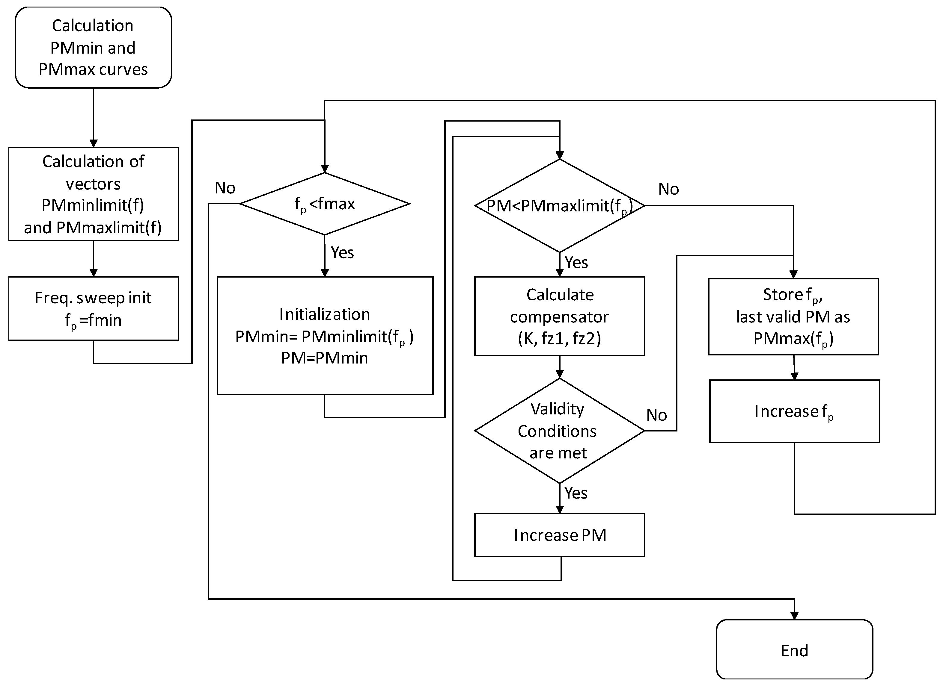
The algorithm to calculate the performance space is described in the flowchart of
Figure 7. It has been elaborated using the theoretical basis provided in
Section 2. The maximum
that can be achieved (PMmax limit in
Figure 6b) can be theoretically calculated as the phase of the uncompensated open-loop transfer function
TU, plus the maximum phase boost that the compensator can provide. On the other hand, there is a limit at low frequencies for the PM (PMmin limit in
Figure 6b), determined by the phase of the uncompensated open-loop transfer function
TU and the minimum phase provided by the compensator (−90 degree in any case). These two boundaries are relevant to reduce the calculations and shorten the calculation time of the performance space [
35]. Once the initial limits of PM have been established, a double sweep is carried out. For each frequency, the value of
PM is initialized and the validity conditions are checked, including those described in
Section 2.2, 0 and 0. If they are met, the value of
PM is increased, and the validity conditions are checked again. Once a non-valid solution is achieved for a given frequency value, the PM loop is interrupted, and the algorithm goes to the next frequency value.
The flowchart in
Figure 7 describes the procedure to calculate the limits of the performance space. Moreover, it can be also used to plot the complete performance space
if PMminlimit(f) and PMmaxlimit(f) are set to the minimum and maximum PM values, respectively, and the validity conditions do not interrupt the loop but are used to classify the solutions.
The most valuable contribution of this algorithm is the ability to analyze all possible designs very quickly and compare different compensator types or the influence of design parameters. The following discussion illustrates this added value.
Limit cycling conditions are analyzed in
Figure 8 in the case of PID compensators. Different types of compensators and design parameters (ratio of zero frequency,
, and
) are considered by running the algorithm of
Figure 7 once per compensator type and design parameter
or
. Note that limit cycling conditions, as described in
Section 2.4, can be easily included in the calculations.
The area limited by the red line in
Figure 8 corresponds to the pairs
that do not meet the integral gain limit cycling condition. This area is smaller, as the separation between the zero frequencies increases (ratio
for PID2 and ratio
for PID1 decrease). The area limited by the green line in the plots of
Figure 8 is the set of solutions that do not meet the limit cycling condition referring to the gain margin. This condition is more related to the frequency itself than to the type of compensator or the value of its design parameter. No significant gains are obtained when the frequencies of the zeros are very different.
Merged results for the PID1 and PID2 compensators are shown in
Figure 9. Areas limited by red or green lines in
Figure 8 are now discarded designs due to the existence of limit cycles. The area limited by the blue line is the performance space free of limit cycling. In the case of PID2, there is a remarkable difference when the frequency of the zeros changes: the lower the ratio
, the wider the allowable performance space. The integral gain limit cycling condition has, in this case, the strongest influence on the allowable designs. PID1 exhibits similar behavior, although the differences are slightly less significant. Both PID1 and PID2 provide similar results when the ratios
or
are very small (0.01 in this case). This fact could be used as a criterion to minimize the possibility of a limit cycle, using a high separation between the frequencies of the zeros (low values of
, and
). However, the response of the system at low frequencies can be degraded, as depicted in
Section 2.5 and as it is confirmed in the experimental measurements. A trade-off should be achieved between the reduction of the area with limit cycling due to integral gain and the degradation of the low-frequency response.
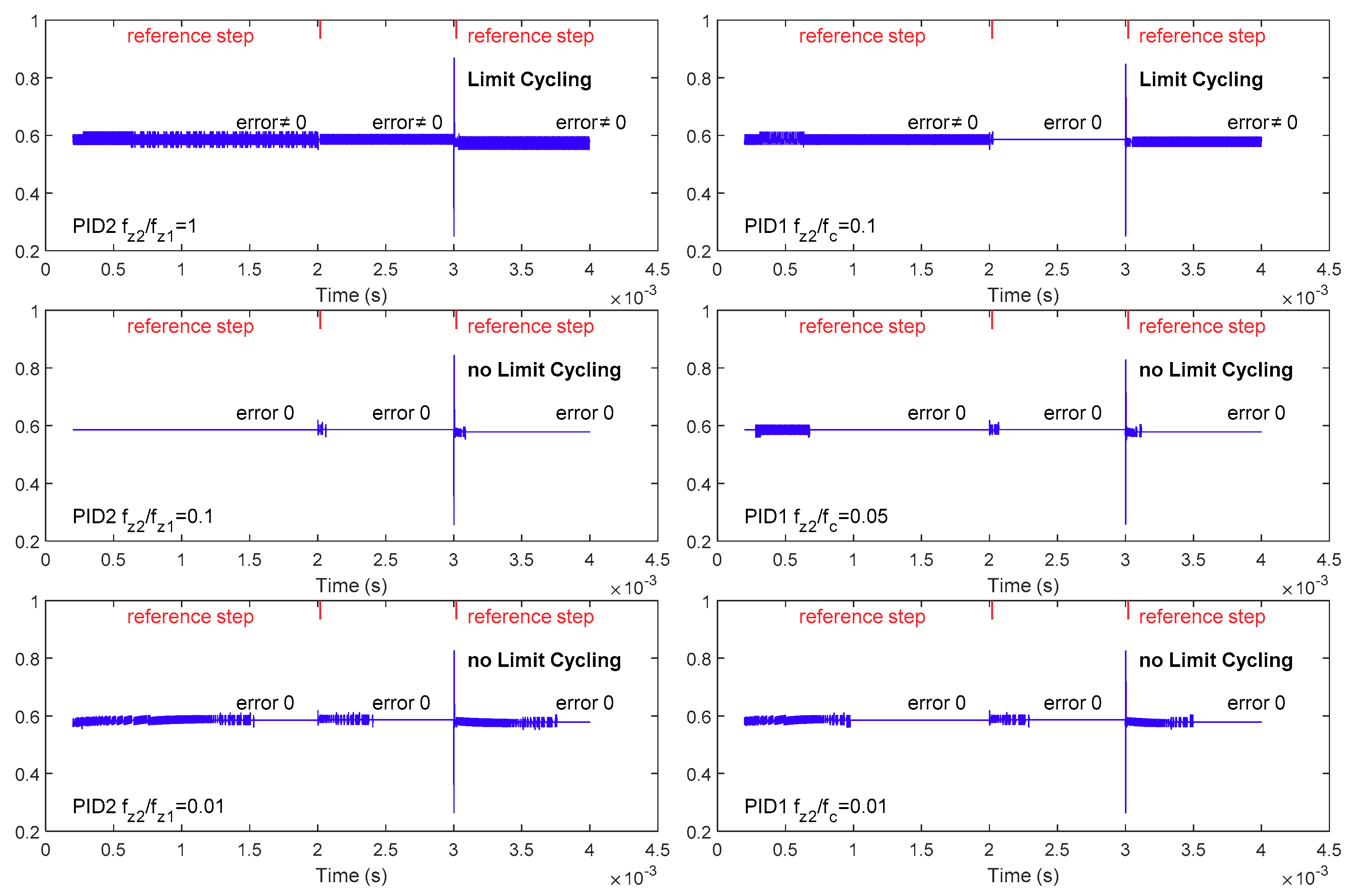
Figure 10 illustrates the limit cycling. Time-domain simulations with a PSIM simulator have been carried out. The ADC and the DPWM (digital PWM) are quantized, but the DPWM has a much higher resolution than the ADC. Therefore, limit cycling concerning the relative resolution of ADC and DPWM [
27] is avoided. Small steps in the output voltage reference are introduced to force transient intervals. After those periods, the system enters into a steady state. If there are still oscillations in the output voltage, there is a limit cycle. As predicted by the performance space of
Figure 9, two of the six analyzed designs (PID2
and PID1
) are outside the performance space in the area corresponding to limit cycling conditions. The other designs do not suffer from limit cycling, agreeing with
Figure 9. Limit cycling failures occur in the case of the lower zero-frequency separation, confirming the trends identified in the previous paragraphs.
A final performance space has been calculated and plotted in
Figure 11. This plot summarizes the best possible design for every dynamic requirement
. Note that all considered compensator topologies cover some area in the performance space.
The first criterion to select the best solution is simplicity: PI is preferred to PID because of the reduced number of coefficients, Equations (12), (15) and (18). The second criterion is the value of index
L, as defined in
Section 2.5—that is, in the case of PID compensators achieving a feasible design for a given specified
, the preferred solution is the one with the lower index
L.
Analyzing this example, the PI is obviously the best solution for a low-frequency requirement. Even if the PID can provide low values of , the PI has a simpler implementation that implies less calculation in the difference equation. Designs using the PI compensator beyond the resonance frequency of the plant are limited to low values of PM, which in practice have no significant interest.
The preferred option for values of beyond the resonance frequency is the PID2 with two zeros at the same frequency. The limitation due to the integral gain limit cycling condition can be overcome using either PID2 or PID1, with higher separation between zero frequencies.
All results presented in this section have been obtained by implementing in Matlab the algorithm to generate the performance space (
Figure 7). Apart from the comparison of different compensators, the same procedure can be used to perform a sensitivity analysis of other parameters, such as time delays and sampling frequency [
35].
4. Experimental Validation
An actual prototype has been built and tested in the laboratory to validate the proposed design procedure, the models, and the assumptions considered in this work. The digital controller has been implemented in a Zybo board, including a Xilinx Zynq-7010 device. An external ADC was used (ADS7476A), limiting the resolution to 10 bits. The specification of the power converter is as follows: input voltage Vin = 8 V, output voltage Vo = 4 V; output inductance L
O = 76 × 10
−6 H; output capacitance C
O = 100 × 10
−6 F; load resistance Ro = 10 Ω; switching frequency fsw = 100 × 10
3 Hz. The transfer function of the power converter G
vd (
Figure 1) has not been calculated, but was measured with a frequency response analyzer. Therefore, all parasitic components (inductor and capacitor series resistances, MOSFET conduction resistance, etc.) are considered in the compensator calculation. The uncompensated loop gain
is shown in
Figure 12, as well as the performance space, without considering the limit cycling conditions. There are some differences with the performance space presented in
Figure 6b due to the differences in the uncompensated open-loop transfer function:
The total time delay produces a significant phase loss beyond the resonance frequency of the uncompensated open loon gain, limiting the feasible solutions at high frequency (PMmax limit). This phase loss is compensated partially by the effect of the equivalent series resistance of the output capacitor;
The Q factor is lower, and so in the performance space, there are possible solutions at crossover frequencies close to the resonance frequency.
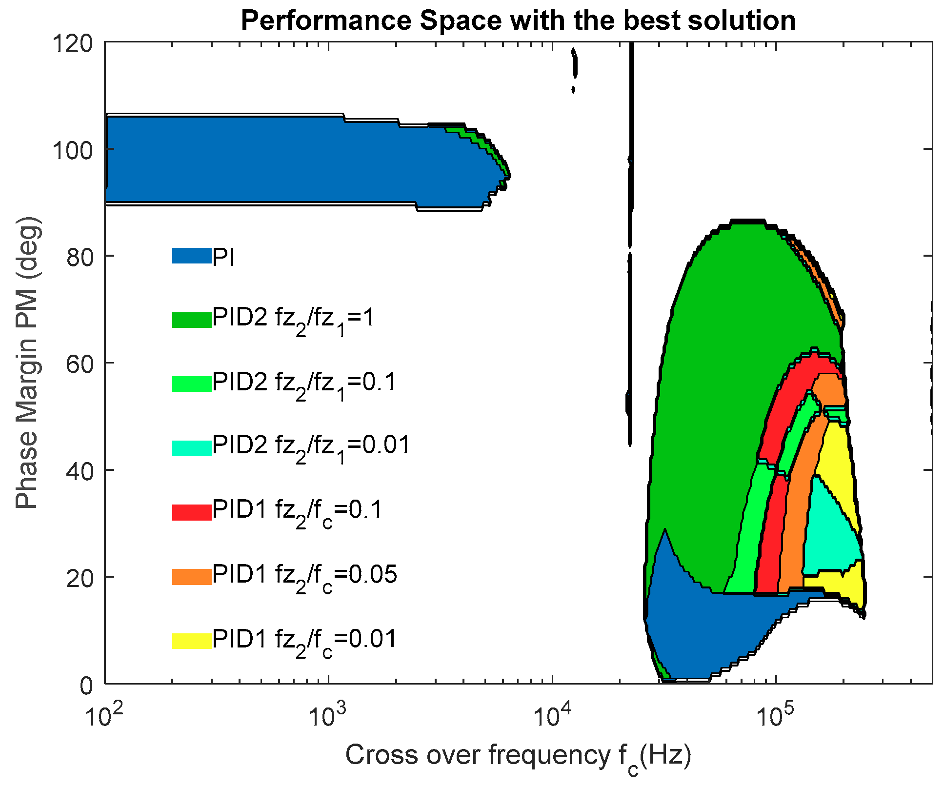
The combination of the performance spaces for the different type of compensators and different design parameters is shown in
Figure 13. In this case, PI ad PID2 with
are the compensator topologies that cover the major part of the area of possible designs. The PID1 topology provides possible designs at high
and low
, where the PID2 with
does not meet the limit cycling condition regarding the integral gain.
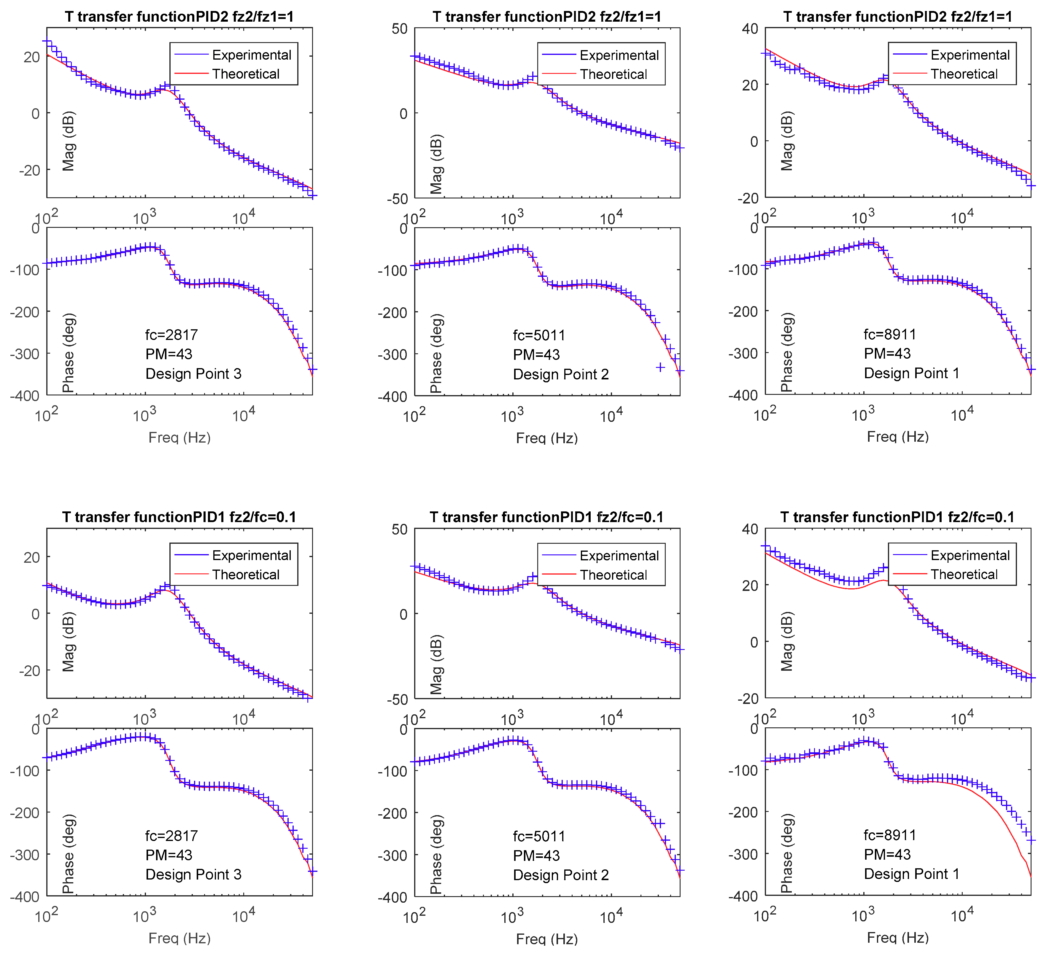
The resulting open-loop gain has been measured in the actual prototype for three dynamic specifications, named as design point 1, 2, and 3, detailed in
Figure 13. For each design point, both PID1 and PID2 have been designed with
and
, respectively. Measurements and theoretical predictions are plotted in
Figure 14, which match very well, especially near the crossover frequency. Another interesting comparison between PID1 and PID2 is the magnitude of the open-loop gain for the same design point. Bellow the cross-frequency in each case, PID2 reaches a higher magnitude than PID1, which means a lower L index. That is why, in the performance space plotted in
Figure 13, PID2 is a better solution than PID1 for the three illustrated design points. This result is also illustrated in the time-domain waveforms appearing in
Figure 15. The output voltage has been measured when a voltage reference step is applied. In the left plot, the six different possibilities for design-point 3 are shown. Although the same crossover frequency and phase margin are selected for the compared waveforms, the system exhibits a different time-response due to the zero location, as shown in previous sections. PID2 with
= 1 is the fastest response, matching with the choice to plot the performance space in
Figure 13. In the right side of
Figure 15, the time-response for design-point 1 for a single compensator is shown to illustrate that, despite the high cross-over frequency, no limit cycles are produced after the transitions, as predicted by the theory.
5. Conclusions
A frequency-based design approach for the calculation of a digital compensator for DC/DC power-switching converters has been presented. It is based on the analytical calculation of the coefficients of the compensator from the dynamic specifications phase margin, PM, and cross-over frequency, , considering the sampling frequency, delay effects, and limit cycling conditions. The approach is focused on the identification of the dynamic specifications that in fact can be achieved, and its graphical representation on a axis. Designs that are not feasible, do not fulfill the requirements, are unstable, or do not meet the limit cycling conditions, are excluded from the performance space.
The design procedure has been automatized. A simple algorithm can generate all feasible designs and plot the performance space. It allows for the identification of the dynamic limitations of a given power converter with a given compensator topology. The most important benefit provided by this approach is the ability to perform a quick and straightforward comparison of compensator topologies or sensitivity analysis of a specific parameter, ensuring the feasibility of the proposed designs.
Three compensator topologies have been considered in the calculations: PI and PID, with two different criteria to establish the frequency of the two zeros (PID1 and PID2). The design procedure has been applied in a particular example, considering seven different compensator types and choosing the more suitable design for each point using a proposed figure of merit calculated from the frequency response.
The described analysis based on the performance space also allows for determination of the simplest compensator design in terms of the dynamic performance, the complexity of the implementation, and the computational resources. In the analyzed example, PI is the best option for low-frequency dynamic requirements. In general, the option covering a larger area in the performance space is PID with two zeros at the same frequency. However, this performance space can be limited by the integral limit cycling condition. Other PID designs with separated zeros can overcome this limitation, but the time response should be assessed. The experimental results of a lab prototype agree with the theoretical predictions.


