Voltage Balance Control Analysis of Three-Level Boost DC-DC Converters: Theoretical Analysis and DSP-Based Real Time Implementation


1
Laboratory of Electric Systems and Telecommunications, Cadi-Ayyad University, BP 549, Av Abdelkarim Elkhattabi, Gueliz, 4000 Marrakesh, Morocco
2
Laboratory of Innovative Technologies, University of Picardie Jules Verne, 80025 Amiens, France
*
Author to whom correspondence should be addressed.
Energies 2018, 11(11), 3073; https://doi.org/10.3390/en11113073
Submission received: 28 September 2018
/
Revised: 14 October 2018
/
Accepted: 26 October 2018
/
Published: 8 November 2018
(This article belongs to the Special Issue Multilevel Converters: Analysis, Modulation, Topologies, and Applications)
Abstract
:In this paper, a step-by-step description to get a unique three-level boost DC–DC converter (TLBDC) (DC—direct current) small signal model is first presented and validated through simulations and experiments. This model allows for overcoming the usage of two sub-models as in the conventional modeling approach. Based on this model, voltage balance (VB) controllers are designed and VB control analysis is presented. Two VB controllers, namely Proportional Integral (PI) and Fuzzy, were analyzed when the VB control was applied on both TLBDC switches or only one. According to the obtained simulation and experimental results, the proposed model gives an accurate approximation in dynamic, small perturbations around an operating point and steady state modes. Moreover, it has been shown that VB is achieved in a reduced time when VB control is applied on both the TLBDC’s switches. Furthermore, the Fuzzy controller performs better than PI controller for VB control.
1. Introduction
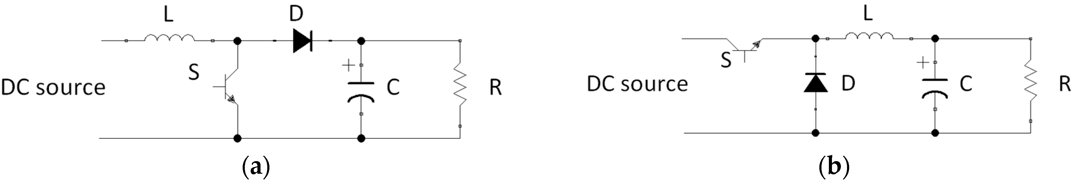
In recent decades, modeling and control of DC–DC (DC—direct current) converters have gained much attention. This is due to their increased uses in various applications, such as voltage regulation [1,2,3,4], renewable energy interfacing [5,6,7], electric vehicle charging [8,9,10], etc. The conventional boost and buck converters are the basic topologies that are shown in Figure 1a,b, respectively. Due to their simplicity and high efficiency, they are the most used DC–DC converters. However, because of high voltage stress on their switching components, these conventional converters are not recommended for medium- and high-voltage ratings that require more powerful switching devices, which increase the cost, the volume, and the system complexity.
Multilevel DC–DC converters are a suitable solution to overcome the aforementioned limitations. This is due to their ability to operate at high power ratings with higher efficiencies compared to conventional two-level topologies. They also provide other advantages such as low distortion of the output voltage and lower switching losses [2,3,4,11,12,13,14]. The three-level DC-DC boost converter (TLBDC) depicted in Figure 2a, has been widely discussed [14,15,16,17,18,19]. The converter fundamentals and design considerations were presented in Reference [19], where it has been shown, for instance, that the converter inductance and capacitors can be significantly reduced when compared to the two-level boost DC–DC converter.
Based on the state-space modeling approach, several TLBDC models were presented [17,18,20,21,22], where two sub-models were used: the first one used for a duty ratio (DR) less than 50%, and the second one is used for a DR greater than 50%. Hence, a selection parameter is required to distinguish between these two sub-models. Using a state space averaged modeling (SSAM) approach and a small signal model (SSM), introduced in Reference [23] and discussed in detail in Reference [3], the transfer functions around a corresponding operating point could be extracted. A discrete-time approach is another way for TLBDC modeling [11,24]. However, it requires long and complex calculations when compared to the previous SSAM method. In Reference [25], a DSP-based implementation of a self-tuning Fuzzy controller for TLBDC has been presented. The converter was modeled using SSAM and three cases based on the DR values were presented: for a DR less than 50%, for a DR higher than 50%, and for any DR. The main objective was the output voltage controller synthesis. However, neither the modeling procedure has been described in detail, nor the simulation and practical model validation were carried out. Moreover, comparison between the single model and the conventional modeling approach was not addressed.
The proper operation of TLBDC needs the balance of the output capacitors’ voltages. Different voltage balance (VB) control methods were presented [15,21,26,27,28,29,30,31,32,33,34]. In References [21,29], and referring to Figure 2, the VB control was achieved by delaying forward or backward SW2 switch control signals of the TLBDC. Another method using an existing energy storage system to ensure the VB was presented in Reference [26]. In References [30,31,32,33,34], the VB control was performed by a PI controller. The controller output was added to the DR of the switch SW1 and subtracted from the DR of switch SW2. A sensor-less VB control method was also proposed in Reference [15] using a PI controller whose output was added to the DR of switch SW2. Finally, in Reference [25], the output capacitors’ voltages were sensed, and a PI-controller was used for VB control. The controller output was added to the SW2 switch DR.
Through this literature review, it is clear that the main VB control methods consist in the following: add a small perturbation to one (or both) converter’s switch(es) DR(s), or adjust the delay between the switches control signals. However, the method to choose the TLBDC switch(es) on which VB control should be applied was not addressed.
Based on these motivations, and unlike Reference [25], where the main goal was the output voltage controller synthesis, this paper adds further contributions to the state of the art by giving a step-by-step description of the followed method to get a unique model for a TLBDC working in continuous conduction mode (CCM), with a non-zero inductor equivalent series resistor. The unique model allows for avoiding the usage of two sub-models as in the conventional modeling approach, and facilitates synthesizing a convenient VB controller. This model has been validated using simulation and experimental tests, and a comparison with the conventional modeling approach is addressed. On the other hand, a technique is presented to best ensure the VB of the TLBDC. The analysis is carried out using two different VB methods and controllers, namely PI and Fuzzy controllers. This allows for figuring out the convenient controller and the adequate way for the VB control of the TLBDC.
The rest of paper is organized as follows. Section 2 describes the TLBDC operation and the developed small signal model (SSM). The VB control of the TLBDC is analyzed in Section 3, followed by the conclusion. Each of Section 2 and Section 3 gives theoretical developments as well as simulation and experimental results.
2. Three-Level Boost DC–DC Converter Small Signal Modeling
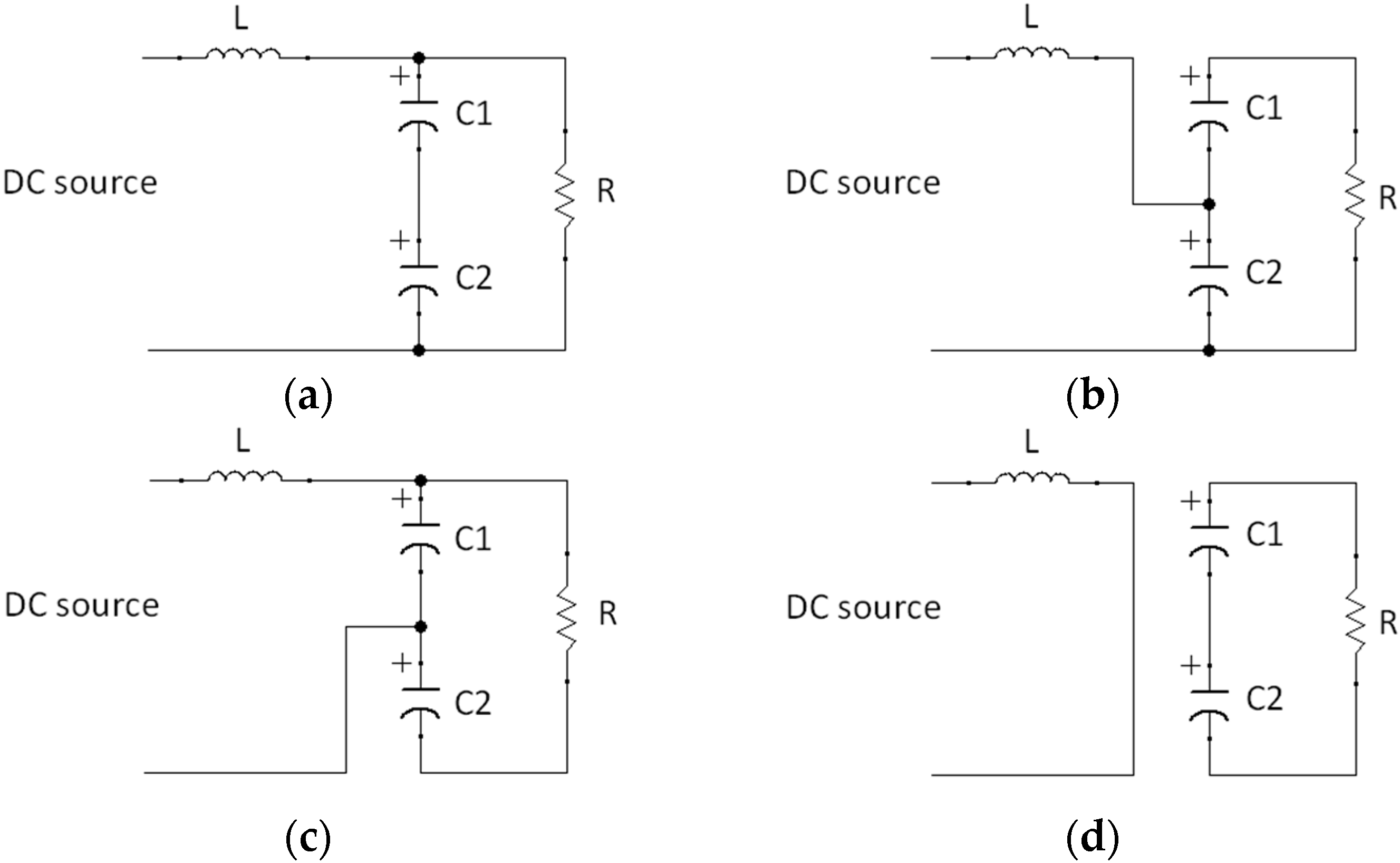
The electrical scheme of the TLBDC under study is shown in Figure 2a. It is composed of an inductor L, two power switches SW1 and SW2, two switching diodes D1 and D2, and finally two output capacitors C1 and C2. u1(t) and u2(t) are the SW1 and SW2 control signals, respectively. These control signals are phase-shifted by 180°, and two operating modes could be distinguished: a DR less than 50% and a DR higher than 50%. The control signals for these two cases are shown in Figure 2b,c, respectively [15,17,18,19,25].
Under CCM, the TLBDC is described by a set of equations and equivalent electrical schemes. These are summarized in Table 1 and Figure 3, respectively. , , , , , and are the inductor current, inductor equivalent series resistor (ESR) (that equals 0.1 Ω in our case), capacitor C1 voltage, capacitor C2 voltage, and input and output voltages, respectively.
Based on the differential Equations (1)–(16), the TLBDC state space equations for the four control signals sequences are given by Equations (17)–(24), where Equations (17) and (18) correspond to the state space equations for 0-0 control signals state, Equations (19) and (20) correspond to the state space equations for 0-1 control signals state, Equations (21) and (22) correspond to the state space equations for 1-0 control signals state, and Equations (23) and (24) correspond to the state space equations for 0-0 control signals state.
Using discrete variables u1(t) and u2(t), Equations (17)–(24) could be assembled into one equation. The obtained TLBDC model is given by Equations (25) and (26).
Equations (25) and (26) could be written as:
Let us denote, , , , and as the average values of the state vector , , , , and , respectively. Using this notation, the obtained SSAM is given by Equations (29) and (30):
Each variable can be written as the sum of small alternating current (AC) variations and DC steady-state quantities as follows:
Using this decomposition, Equations (31)–(35), Equations (29) and (30) become:
where: , , and .
Neglecting the higher-order terms, steady-state terms are null, and supposing that the supply voltage is constant, terms written in bold, italic, and bold italic in Equation (36), respectively [3]. The SSM of the TLBDC is given by Equations (38) and (39):
The proposed model is validated through simulation and experimental results. Simulations were performed on MATLAB software (Matworks, Natick, MA, USA) using the ode23 function, while the experimental tests were carried out on the experimental setup depicted in Section 3. The TLBDC parameters used for these tests are listed in Table 2.
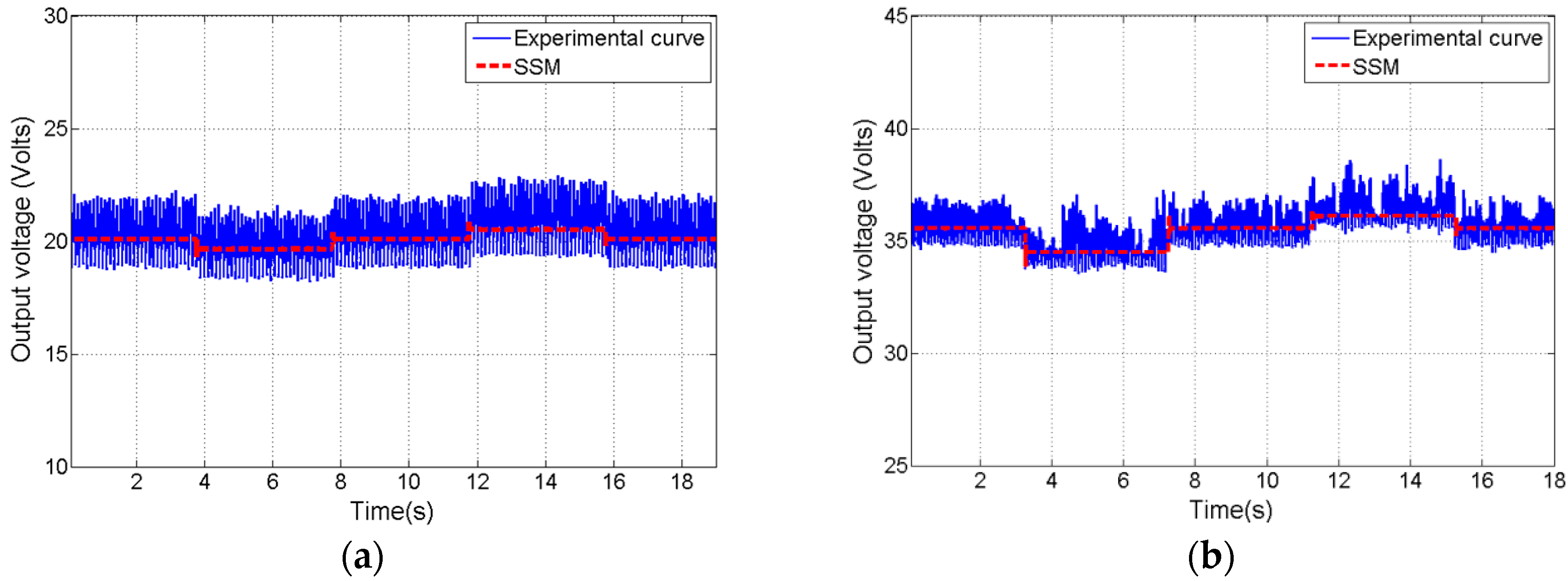
The simulated and experimental output voltage curves for the switched model and the SSM around 30% and 60% DRs are respectively illustrated in Figure 4 and Figure 5, where 4% positive and negative perturbations were introduced around those DR values.
Based on the results reported in Figure 4, it can be seen that the SSM behavior was in accordance with the switched one. In addition, the presented experimental results in Figure 5 were closely matching those obtained from the proposed SSM. By analyzing these results, one can see that the proposed SSM gave an averaged behavior of the TLBDC for both DR cases.
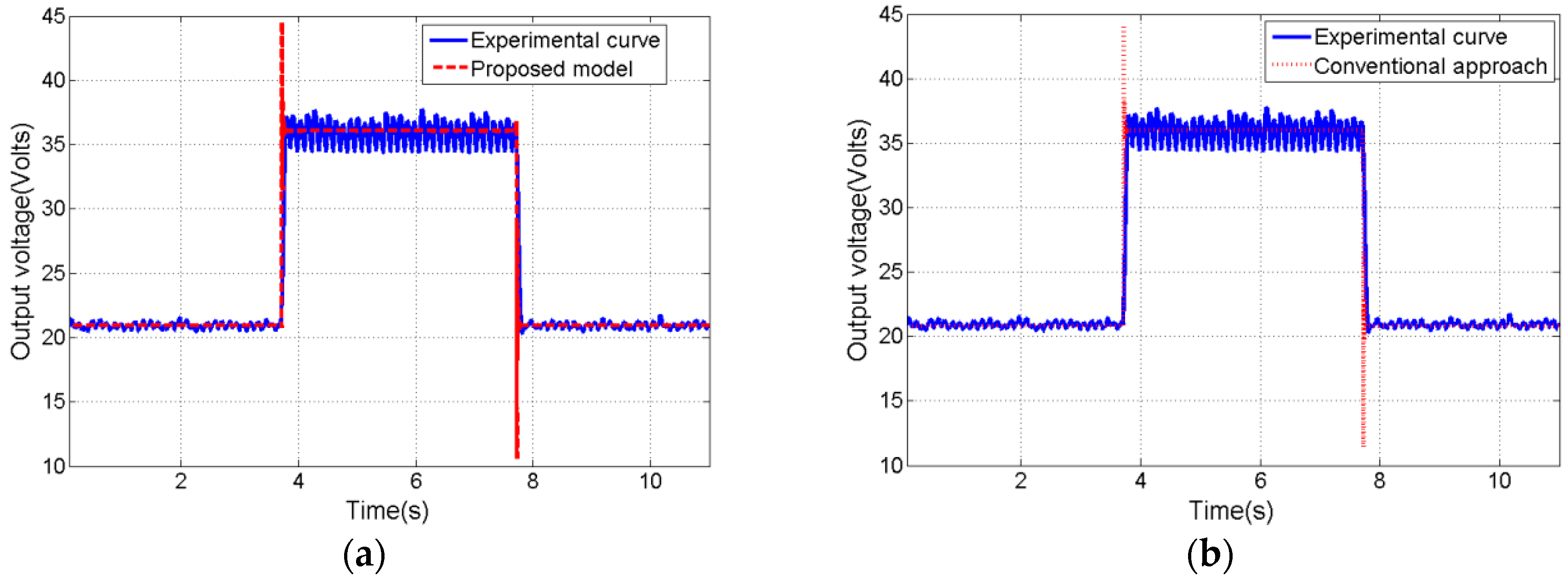
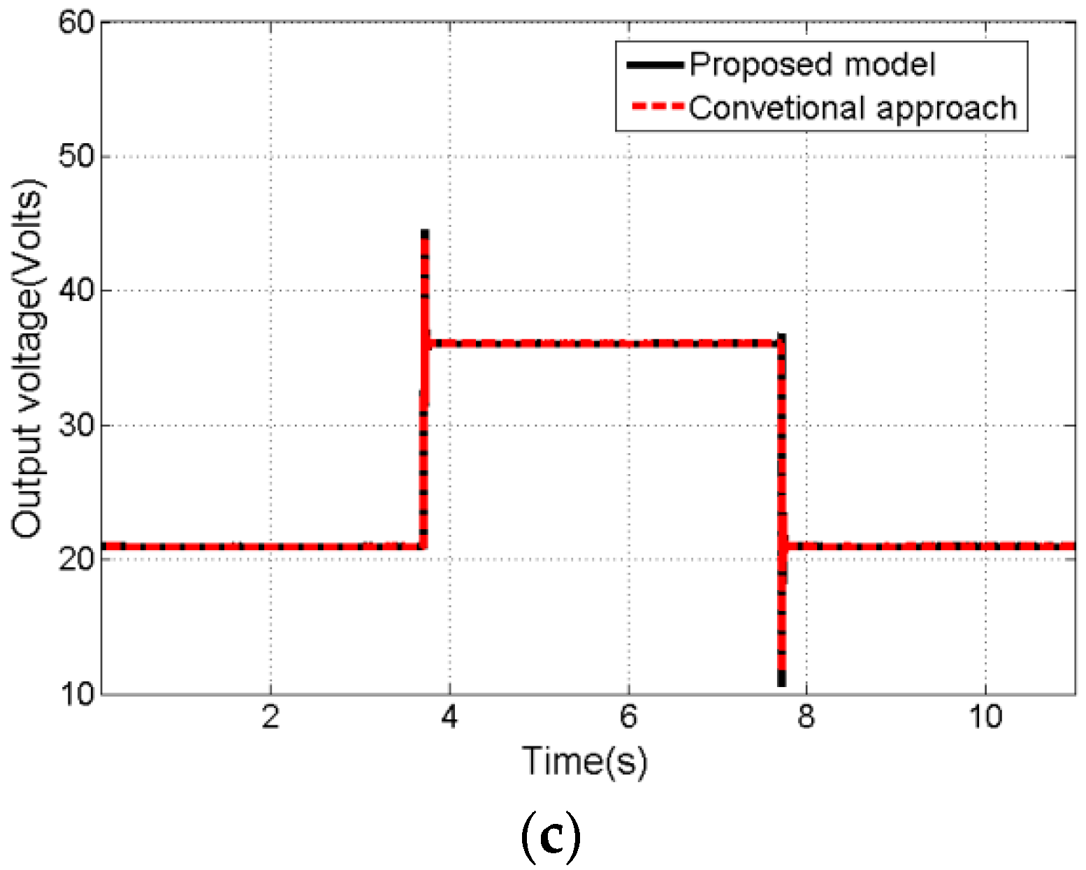
The results for a DR transition from a value less than 50%, namely 30%, to another one higher than 50%, namely 60%, are shown in Figure 6. The proposed SSAM and experimental output voltage curves are shown in Figure 6a, while Figure 6b illustrates the conventional SSAM and experimental output voltage curves. Finally, Figure 6c presents a comparison between the conventional approach and the proposed one.
By analyzing the results depicted in Figure 6, the model behavior when the DR was changed from a value less than 50% to another one higher than 50% is similar to the conventional one. Both SSAM approaches had identical output voltage curves, but the conventional approach used two different sub-models for the two duty ratio ranges, 0–50% and 50–100%, which required an additional selection parameter that allowed for choosing the convenient model [17,18,20,21,22]. Additionally, unlike the previous works [17,18,20,21,22,25], the followed procedure for TLBDC modeling was described in step-by-step detail.
Applying Laplace transforms with zero initial conditions and using the superposition theorem, the small-signal duty-cycles and to state vector transfer functions are as follows [3,24,35]:
The transfer functions, , , , and can be deduced, and the required VB controllers are then designed.
3. Three-Level Boost DC–DC Converter Voltage Balance Control (VBC) Analysis
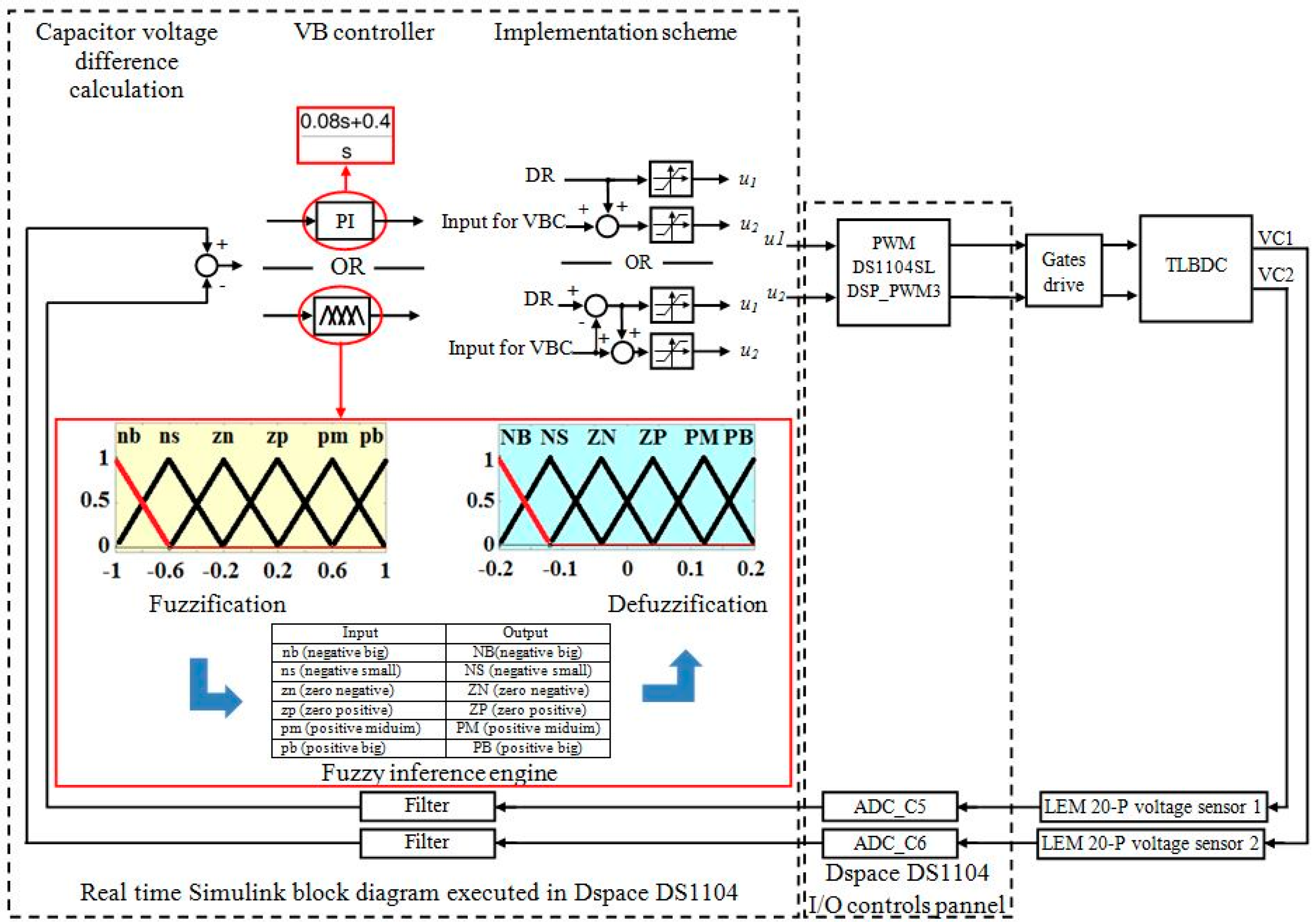
In order to assess the suitable method/controller for the VB control of the TLBDC, a comparison between two different methods using two different controllers, PI and Fuzzy, is carried out. The DR is set by an outer control loop, and the PI/Fuzzy controller ensures the VB control. The VB controllers’ parameters are illustrated in Figure 7. The VB control is applied on both switches by subtracting the VB controller output from SW1 DR and adding it to SW2 DR, or on the lower switch only, by adding it to SW2 DR as illustrated in Figure 7. The duty cycles u1 and u2 are then used to generate the SW1 and SW2 control signals, respectively. SW1 and SW2 control signals are phase shifted by 180° as previously shown in Figure 2b,c.
The aforementioned comparisons were examined via simulations performed in Matlab/Simulink software (Matworks, Natick, MA, USA), while the experimental tests were performed on the TLBDC prototype shown in Figure 8. The simplified scheme of the experimental setup and the TLBDC parameters are shown in Figure 9 and Table 2, respectively.
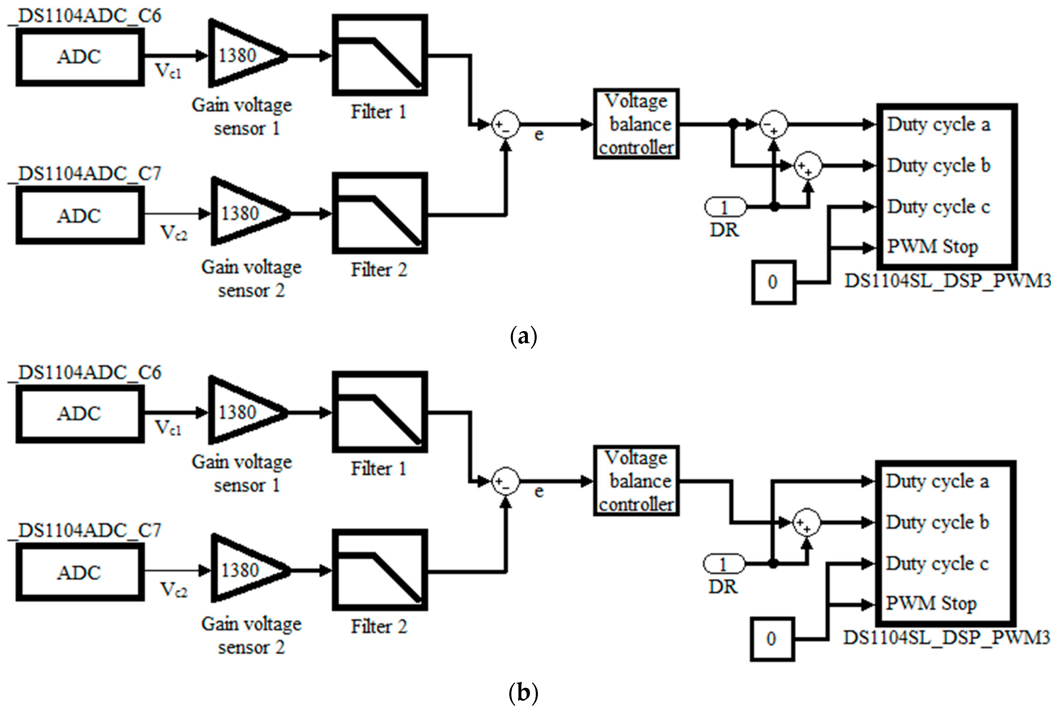
VB control was implemented using the dSPACE 1104. After building the TLBDC VBC based on real-time Simulink-blocks, including the dSPACE 1104 slave-PWM generator and analog to digital (A/D) converters, the C code was automatically generated, downloaded and executed on the dSPACE board. The 180° phase-shifted control signals were generated using the dSPACE 1104. The logic signals were provided to an IR2110 gate driver that allowed for controlling the two TLBDC’s MOSFETs (Metal–Oxide–Semiconductor Field-Effect Transistors). The dSPACE DS1104 ControlDesk monitor software was used to visualize and save the experimental data. The implemented Matlab/Simulink models on the dSPACE DS1104 board are shown in Figure 10, where Figure 10a illustrates the implemented model when the VB was applied on the lower switch of TLBDC, and Figure 10b shows the implemented model when the VB control was applied on both TLBDC switches. The VB controller, indicated in Figure 10, was either a Fuzzy or PI controller whose parameters are shown in Figure 7.
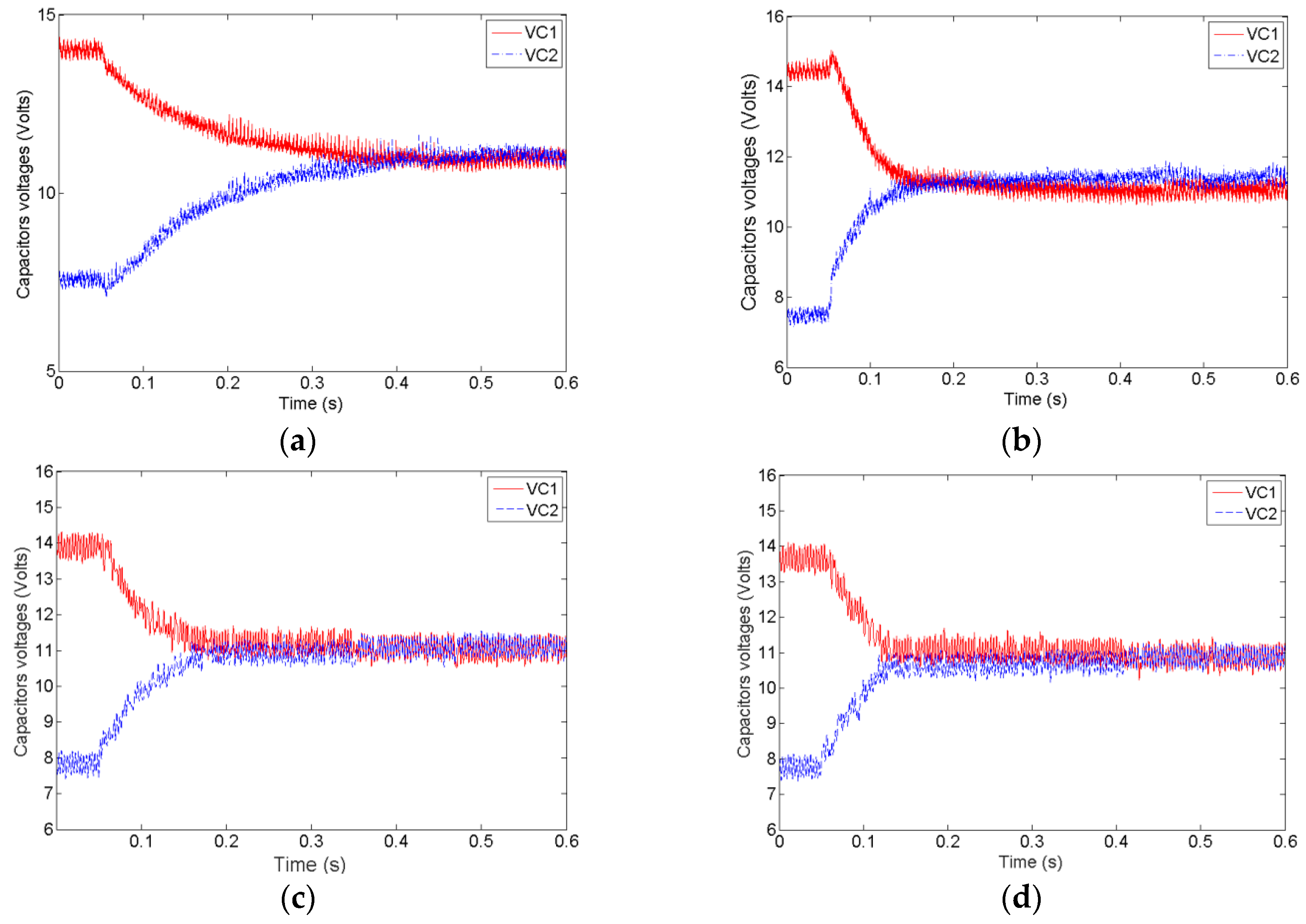
Simulation and experimental results are depicted in Figure 11 and Figure 12, respectively. Simulated output capacitors’ voltages before and after applying the VB control at t = 0.025 s are presented in Figure 11. Using a PI controller, the VB was approximately achieved in 5 ms and 15 ms when the VBC was applied on both TLBDC switches, or only one, respectively. While the Fuzzy controller ensured a VB within 3 ms and 10 ms when the VBC was applied on both switches or on the lower switch, respectively. The same results could be deduced from experimental results presented in Figure 12, where the VB control was applied at t = 0.05 s. The VB, using a PI controller, was achieved in approximately 0.1 s and 0.3 s, when applying the VB control on both switches or one switch, respectively. While it was approximately achieved, using a Fuzzy controller, within 0.08 s and 0.15 s when the VB control was applied on both switches or on the lower switch, respectively.
According to the previous results, static and dynamic behaviors of the proposed model are in agreement with the experiments. The slight observed differences were mainly caused by the simplified assumptions made in the analysis, the slight errors introduced by measuring instruments, etc.
By analyzing the obtained results from the VB control analysis, one can see that the experimental results were in good agreement with the simulated ones. The differences observed in the VB controller’s response times, in simulations and experiments, were mainly due to delays included by the digital to analogue (D/A) conversions, the processing time for real time implementation, and the needed time for the voltage average value calculation loop.
The analysis has shown that a VB was ensured in all cases. However, for both controllers, applying the VB control on either of the TLBDC’s switches allows achieving the VB within a reduced time compared to applying it on one switch only. This showed that the works presented in References [29,30,31,32,33], where a VB control was applied on both TLBDC switches, have used an efficient way to ensure a VB control. In addition, the Fuzzy VB controller showed better performances compared to the PI controller, in terms of the requested time to ensure a VB for both cases as indicated in Table 3.
4. Summary and Conclusions
The results of this study present a significant advance in the modeling and control of TLBDCs. This research also fills the gap in the related literature concerning this topic and provides new findings. The TLBDC unique model that describes the converter behavior for all DR values was first described in details. Based on the TLBDC switches’ states and their equivalent electrical schemes, the state-space modeling of a non-zero inductor ESR TLBDC was carried out, and its SSM was then derived and validated using a TLBDC prototype. In a second stage, a VB control analysis was presented. Two VB controllers, PI and Fuzzy types, were used and their outputs were applied on both or one TLBDC switch(es), respectively. This allowed for choosing the efficient way and convenient controller for the TLBDC VB control.
The obtained results showed a good agreement between simulations and experiments. They also demonstrated that the developed model gave an accurate estimation of the TLBDC behavior. Generally, the presented results reflected an accurate approximation of the real results in dynamic, small perturbations around a corresponding operating point, and steady-state modes. These results have also shown that VB was achieved in all cases. However, applying the VB control on both switches allowed for achieving a VB in a reduced time compared to applying it on one switch. In addition, the Fuzzy controller presented good results, in terms of required time to ensure a VB control, when compared to the PI VB controller.
Author Contributions
Conceptualization, D.O.-A., S.D. and A.R.; Methodology, D.O.-A., S.D. and A.R.; Software, D.O.-A., S.D. and A.R.; Validation, D.O.-A., S.D. and A.R.; Writing—Original Draft Preparation, D.O.-A.; Writing—Review and Editing, D.O.-A., A.R. and S.D.; Supervision, S.D. and A.R.; Funding Acquisition, S.D. and A.R.
Funding
This work is performed in the framework of VERES Project funded by the Research Institute in Solar Energy and New Energies (IRESEN).
Conflicts of Interest
The authors declare no conflict of interest.
References
- Sun, Y.; Ma, L.; Zhao, D.; Ding, S. A Compound Controller Design for a Buck Converter. Energies 2018, 11, 2354. [Google Scholar] [CrossRef]
- Rashid, M.H. Power Electronics Handbook, 3rd ed.; Butterworth-Heinemann: Oxford, UK, 2011. [Google Scholar]
- Monmasson, E. Power Electronic Converters-PWM Strategies and Current Control Techniques; ISTE Ltd.: London, UK, 2011. [Google Scholar]
- Gerard, V.P.; Eduard, A. CMOS Integrated Switching Power Converters; Springer: New York, NY, USA, 2009. [Google Scholar]
- Reza Tousi, S.M.; Moradi, M.H.; Basir, N.S.; Nemati, M. A function-based maximum power point tracking method for photovoltaic systems. IEEE Trans. Power Electron. 2016, 31, 2120–2128. [Google Scholar] [CrossRef]
- Hossain, M.Z.; Rahim, N.A.; Selvaraj, J. A/L Recent progress and development on power DC-DC converter topology, control, design and applications: A review. Renew. Sustain. Energy Rev. 2018, 81, 205–230. [Google Scholar] [CrossRef]
- Patel, H.; Agarwal, V. Maximum power point tracking scheme for PV systems operating under partially shaded conditions. IEEE Trans. Ind. Electron. 2008, 55, 1689–1698. [Google Scholar] [CrossRef]
- Miao, K.; Ramachandaramurthy, V.K.; Yong, J.Y. Integration of electric vehicles in smart grid: A review on vehicle to grid technologies and optimization techniques. Renew. Sustain. Energy Rev. 2016, 53, 720–732. [Google Scholar]
- Goli, P.; Shireen, W. PV powered smart charging station for PHEVs. Renew. Energy 2014, 66, 280–287. [Google Scholar] [CrossRef]
- Torreglosa, J.P.; Fern, L.M.; García-trivi, P.; Jurado, F. Control and operation of power sources in a medium-voltage direct- current microgrid for an electric vehicle fast charging station with a photovoltaic and a battery energy storage system. Energy 2016, 115, 38–48. [Google Scholar]
- El Aroudi, A.; Robert, B.; Martinez-Salamero, L. Modelling and analysis of multi-cell converters using discrete time models. In Proceedings of the IEEE International Symposium on Circuits and Systems, Island of Kos, Greece, 21–24 May 2006; pp. 2161–2164. [Google Scholar]
- Zhang, Y.; Shi, J.; Fu, C.; Zhang, W.; Wang, P.; Li, J.; Sumner, M. An Enhanced Hybrid Switching-Frequency Modulation Strategy for Fuel Cell Vehicle Three-Level DC-DC Converters with Quasi-Z Source. Energies 2018, 11, 1026. [Google Scholar] [CrossRef]
- Hafez, A.A.A. Multi-level cascaded DC/DC converters for PV applications. Alex. Eng. J. 2015, 54, 1135–1146. [Google Scholar] [CrossRef]
- Zajec, P.; Nemec, M. Theoretical and Experimental Investigation of the Voltage Ripple across Flying Capacitors in the Interleaved Buck Converter with Extended Duty Cycle. Energies 2018, 11, 1017. [Google Scholar] [CrossRef]
- Chen, H.C.; Lin, W.J. MPPT and voltage balancing control with sensing only inductor current for photovoltaic-fed, three-level, boost-type converters. IEEE Trans. Power Electron. 2014, 29, 29–35. [Google Scholar] [CrossRef]
- Zhang, Y.; Sun, J.T.; Wang, Y.F. Hybrid boost three-level DC-DC converter with high voltage gain for photovoltaic generation systems. IEEE Trans. Power Electron. 2013, 28, 3659–3664. [Google Scholar] [CrossRef]
- Bougrine, M.D.; Benalia, A.; Benbouzid, M.H. Simple sliding mode applied to the three-level boost converter for fuel cell applications. In Proceedings of the International Conference on Control, Engineering and Information Technology, Tlemcen, Algeria, 25–27 May 2015; pp. 1–6. [Google Scholar]
- Yaramasu, V.; Wu, B. Predictive control of a three-level boost converter and an NPC inverter for high-power PMSG-based medium voltage wind energy conversion systems. IEEE Trans. Power Electron. 2014, 29, 5308–5322. [Google Scholar] [CrossRef]
- Ruan, X.; Li, B.; Chen, Q.; Tan, S.C.; Tse, C.K. Fundamental considerations of three-level DC-DC converters: Topologies, analyses, and control. IEEE Trans. Circuits Syst. I Regul. Pap. 2008, 55, 3733–3743. [Google Scholar] [CrossRef] [Green Version]
- Ma, H.; Yang, C.; Zhang, Y.Y. Analysis and design for single-phase three-level boost PFC converter with quasi-static model. In Proceedings of the 37th Annual Conference of the IEEE Industrial Electronics Society, Melbourne, VIC, Australia, 7–10 November 2011; pp. 4385–4390. [Google Scholar]
- Krishna, R.; Soman, D.E.; Kottayil, S.K.; Leijon, M. Pulse delay control for capacitor voltage balancing in a three-level boost neutral point clamped inverter. IET Power Electron. 2015, 8, 268–277. [Google Scholar] [CrossRef]
- Meleshin, V.; Sachkov, S.; Khukhtikov, S. Three-level boost converters. Modes, sub-modes and asymmetrical regime of operation. In Proceedings of the 16th European Conf. on Power Electronics and Applications, Lappeenranta, Finland, 26–28 August 2014; pp. 1–10. [Google Scholar]
- Middlebrook, R.D.; Cuk, S. A general unified approach to modelling switching-converter power stages. In Proceedings of the Power Electronics Specialists Conference, Cleveland, OH, USA, 8–10 June 1976; pp. 18–34. [Google Scholar]
- Khaldi, H.S.; Ammari, A.C. Fractional-order control of three level boost DC/DC converter used in hybrid energy storage system for electric vehicles. In Proceedings of the 6th International Renewable Energy Congress, Sousse, Tunisia, 24–26 March 2015; pp. 1–7. [Google Scholar]
- Nouri, A.; Salhi, I.; Elwarraki, E.; El Beid, S.; Essounbouli, N. DSP-based implementation of a self-tuning fuzzy controller for three-level boost converter. Electr. Power Syst. Res. 2017, 146, 286–297. [Google Scholar] [CrossRef]
- Rivera, S.; Wu, B. Electric Vehicle Charging Station with an Energy Storage Stage for Split-DC Bus Voltage Balancing. IEEE Trans. Power Electron. 2016, 32, 2376–2386. [Google Scholar] [CrossRef]
- Tan, L.; Zhu, N.; Wu, B. An Integrated Inductor for Eliminating Circulating Current of Parallel Three-Level DC–DC Converter-Based EV Fast Charger. IEEE Trans. Ind. Electron. 2016, 63, 1362–1371. [Google Scholar] [CrossRef]
- Tan, L.; Wu, B.; Yaramasu, V.; Rivera, S.; Guo, X. Effective Voltage Balance Control for Bipolar-DC-Bus-Fed EV Charging Station With Three-Level DC–DC Fast Charger. IEEE Trans. Ind. Electron. 2016, 63, 4031–4041. [Google Scholar] [CrossRef]
- Vitoi, L.A.; Krishna, R.; Soman, D.E.; Leijon, M.; Kottayil, S.K. Control and implementation of three level boost converter for load voltage regulation. In Proceedings of the Industrial Electronics Society Conference, Vienna, Austria, 10–13 November 2013; pp. 561–565. [Google Scholar]
- Tan, L.; Wu, B.; Rivera, S.; Yaramasu, V. Comprehensive DC Power Balance Management in High-Power Three-Level DC–DC Converter for Electric Vehicle Fast Charging. IEEE Trans. Power Electron. 2016, 31, 89–100. [Google Scholar] [CrossRef]
- Xia, C.; Gu, X.; Shi, T.; Yan, Y. Neutral-Point Potential Balancing of Three-Level Inverters in Direct-Driven Wind Energy Conversion System. IEEE Trans. Energy Convers. 2011, 26, 18–29. [Google Scholar] [CrossRef]
- Oulad-Abbou, D.; Doubabi, S.; Rachid, A.; García-Triviño, P.; Fernández-Ramírez, L.M.; García-Vázquez, C.A.; Sarrias-Mena, R. Combined control of MPPT, output voltage regulation and capacitors voltage balance for three-level DC/DC boostconverter in PV-EV charging stations. In Proceedings of the International Symposium on Power Electronics, Electrical Drives, Automation and Motion (SPEEDAM), Amalfi, Italy, 20–22 June 2018; pp. 372–376. [Google Scholar]
- Costa, L.F.; Mussa, S.A.; Barbi, I. Capacitor voltage balancing control of multilevel DC-DC converter. In Proceedings of the Brazilian Power Electronics Conference, Gramado, Brazil, 27–31 October 2013; pp. 332–338. [Google Scholar]
- Zhao, Q.; Fang, Y.; Ma, M.; Wang, J.; Xie, Y. Study on a Fuzzy Controller for the Balance of Capacitor Voltages of Three-Level Boost Dc-Dc Converter. In Proceedings of the International Power Electronics and Application Conference and Exposition (PEAC), Shanghai, China, 5–8 November 2014; pp. 993–996. [Google Scholar]
- Mobarrez, M.; Ghanbari, N. Subhashish Bhattacharya Control Hardware-in-the-Loop Demonstration of a Building-Scale DC Microgrid Utilizing Distributed Control Algorithm. In Proceedings of the PES General Meeting 2018, Portland, OR, USA, 5–9 August 2018. [Google Scholar]
Figure 1.
Conventional two-level schemes: (a) a boost converter, and (b) a buck converter.

Figure 2.
(a) The electrical scheme of the TLBDC under study, (b) TLBDC control signals for a DR less than 50%, and (c) TLBDC control signals for a DR higher than 50%.
Figure 2.
(a) The electrical scheme of the TLBDC under study, (b) TLBDC control signals for a DR less than 50%, and (c) TLBDC control signals for a DR higher than 50%.
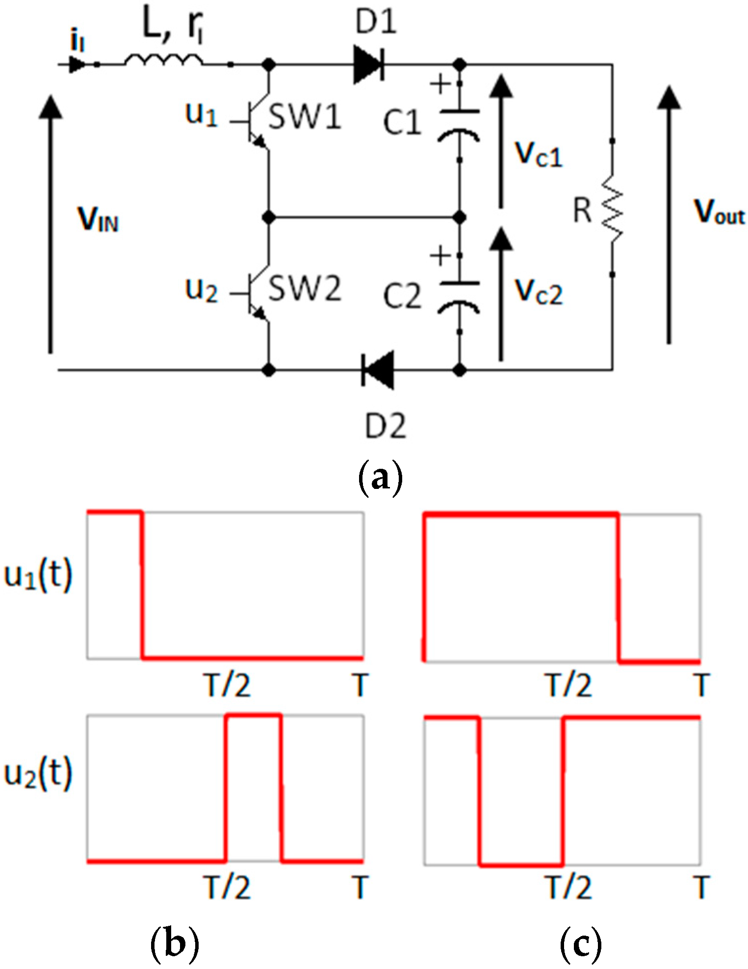
Figure 3.
TLBDC equivalent electrical schemes for control signals u1(t)-u2(t) sequence: (a) 0-0, (b) 1-0, (c) 0-1 and (d) 1-1.
Figure 3.
TLBDC equivalent electrical schemes for control signals u1(t)-u2(t) sequence: (a) 0-0, (b) 1-0, (c) 0-1 and (d) 1-1.

Figure 4.
Simulated SSM and switched model output voltage curves in the case of 4% DR perturbation: (a) around 30%, and (b) around 60% DRs.
Figure 4.
Simulated SSM and switched model output voltage curves in the case of 4% DR perturbation: (a) around 30%, and (b) around 60% DRs.
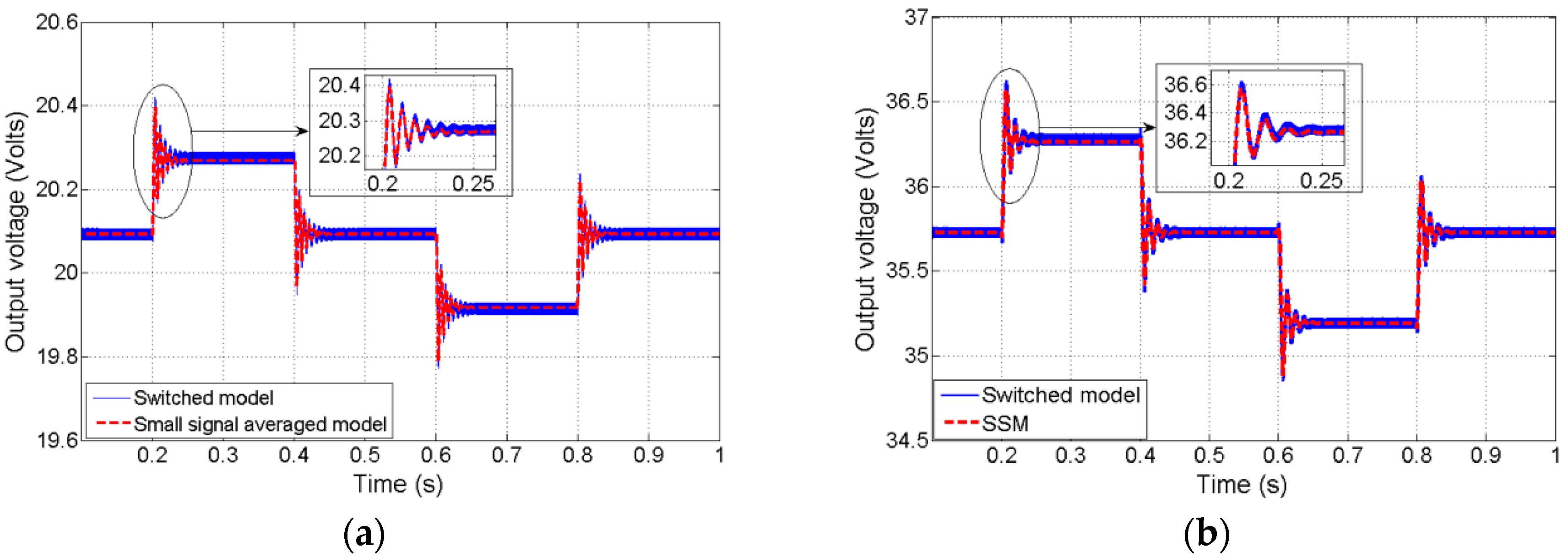
Figure 5.
Experimental and SSM output voltages curves with 4% perturbation width: (a) around thirty percent and (b) around sixty percent DRs.
Figure 5.
Experimental and SSM output voltages curves with 4% perturbation width: (a) around thirty percent and (b) around sixty percent DRs.

Figure 6.
Curves for a DR value change from 30% to 60% to 30%: (a) proposed model and experimental output voltages, (b) experimental and conventional approach output voltages, and (c) proposed and conventional approach output voltages.
Figure 6.
Curves for a DR value change from 30% to 60% to 30%: (a) proposed model and experimental output voltages, (b) experimental and conventional approach output voltages, and (c) proposed and conventional approach output voltages.


Figure 7.
Block diagram of voltage balance control (VBC) schemes.

Figure 8.
TLBDC Experimental setup.
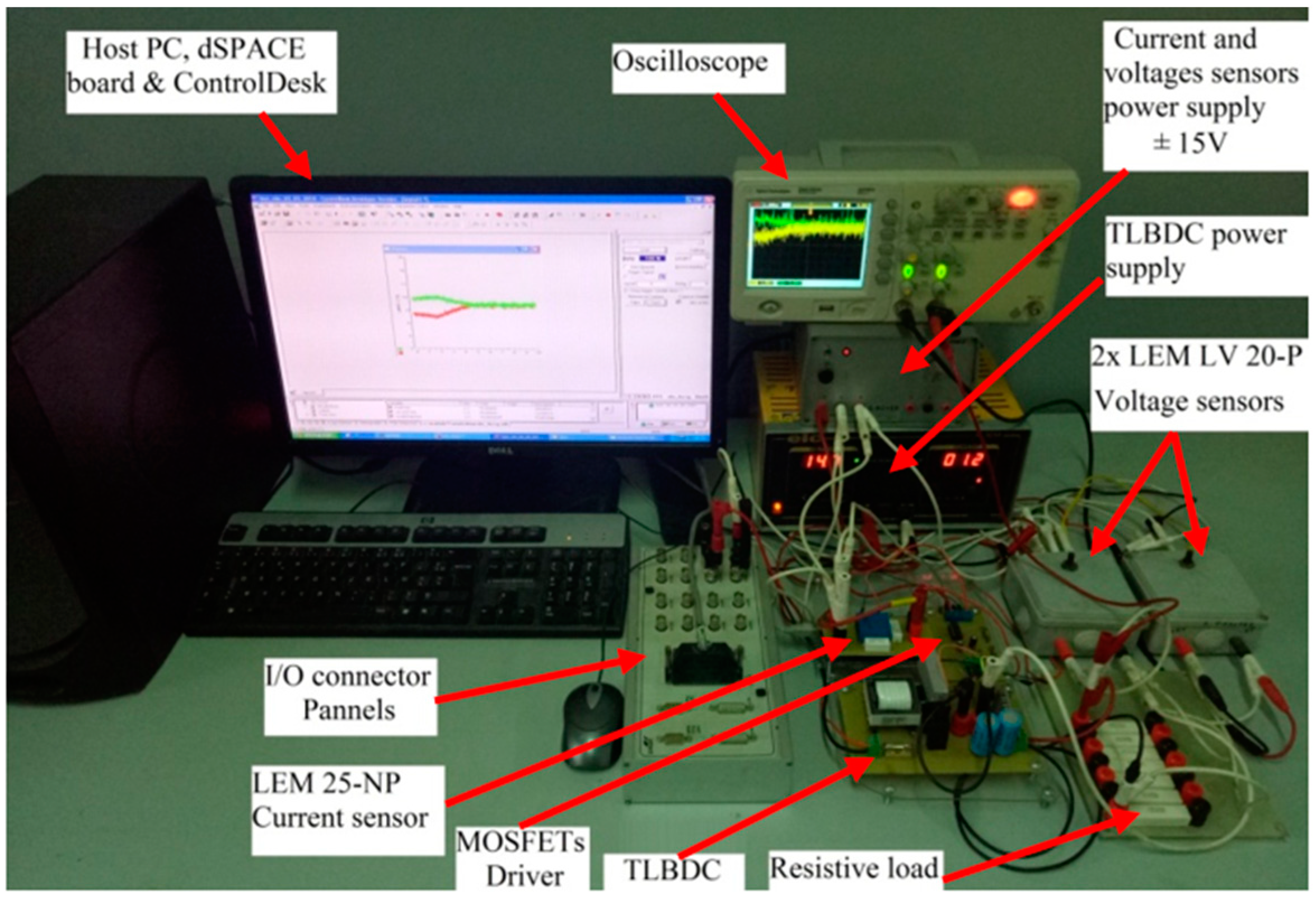
Figure 9.
Block-diagram of the dSPACE DS1104 controller board.
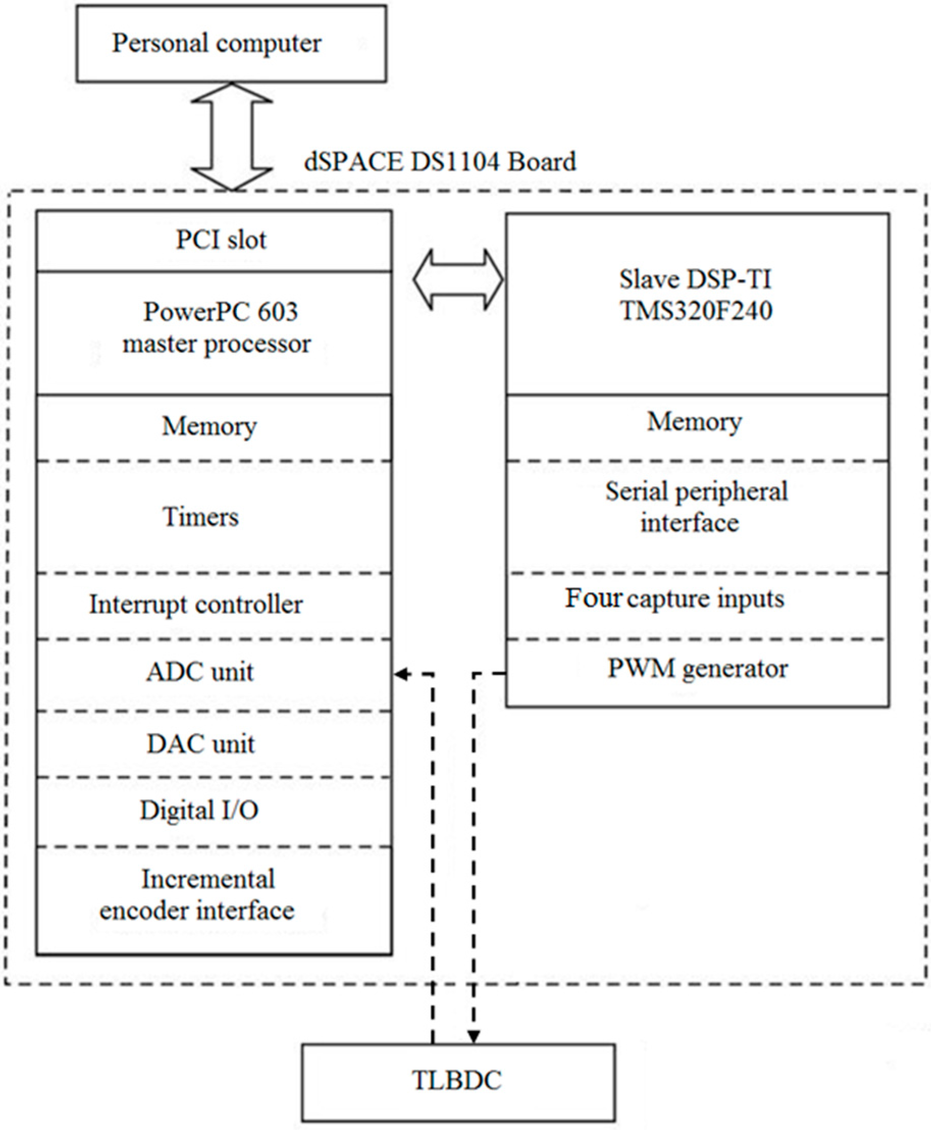
Figure 10.
Matlab/Simulink implemented model on the dSPACE DS1104 board: (a) VB control applied on the TLBDC lower switch, and (b) VB control applied on either switche of the TLBDC.
Figure 10.
Matlab/Simulink implemented model on the dSPACE DS1104 board: (a) VB control applied on the TLBDC lower switch, and (b) VB control applied on either switche of the TLBDC.

Figure 11.
Simulated output capacitors’ voltage curves after applying a balancing control at t = 0.025 s: (a) on both switches using a PI VB controller, and (b) on the lower switch using a PI VB controller, (c) on both switches using a Fuzzy VB controller, and (d) on the lower switch using a Fuzzy VB controller.
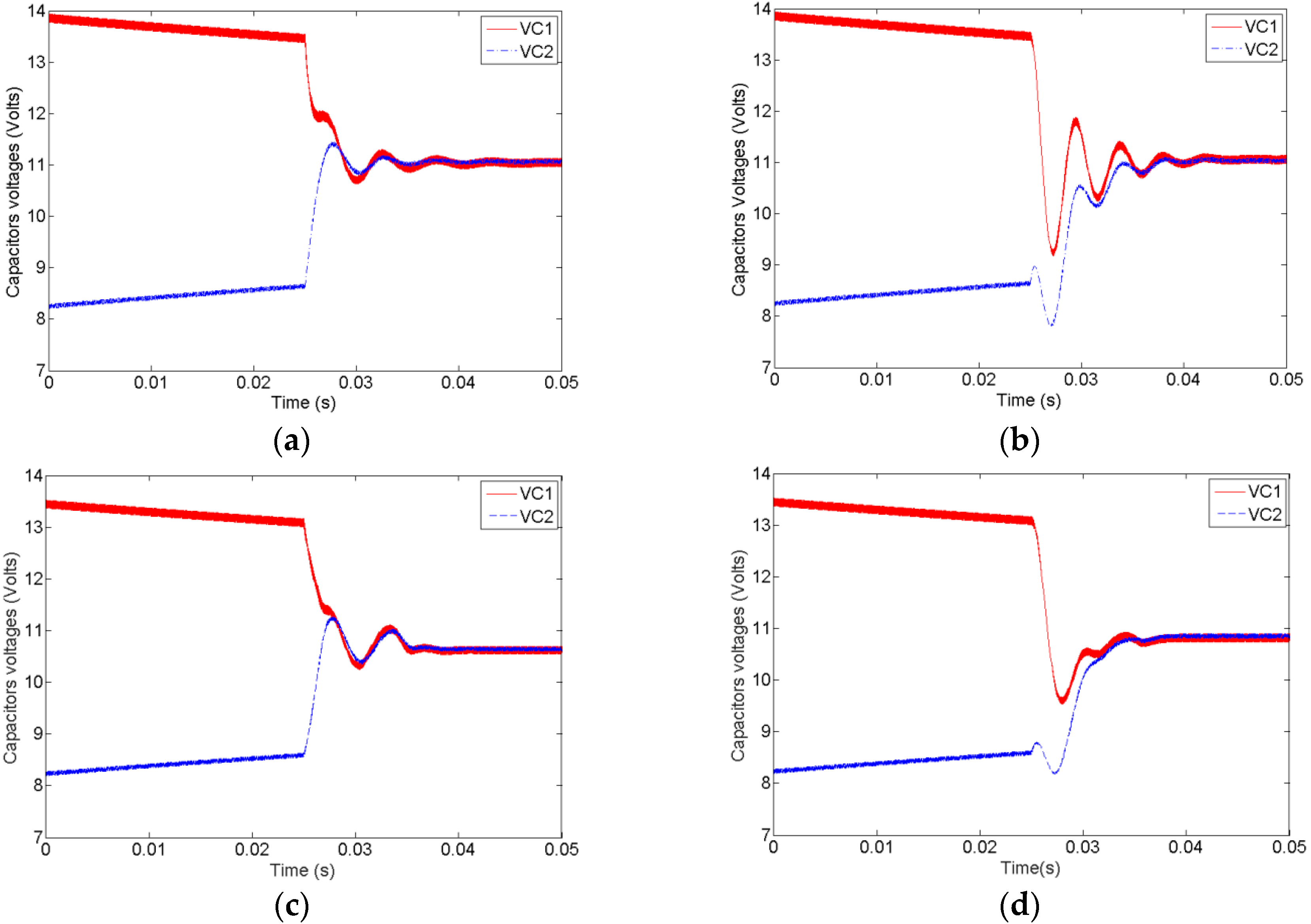
Figure 12.
Experimental output capacitors’ voltage curves: (a) on both switches using a PI VB controller, and (b) on the lower switch using a PI VB controller, (c) on both switches using a Fuzzy VB controller, and (d) on the lower switch using a Fuzzy VB controller.
Figure 12.
Experimental output capacitors’ voltage curves: (a) on both switches using a PI VB controller, and (b) on the lower switch using a PI VB controller, (c) on both switches using a Fuzzy VB controller, and (d) on the lower switch using a Fuzzy VB controller.


Table 1.
Differential equations for each control signals sequence of TLBDC working in CCM.
| State of the Control Signals (u1(t)-u2(t)) | Differential Equations |
|---|---|
| 0-0 | |
| 1-0 | |
| 0-1 | |
| 1-1 |
Table 2.
TLBDC parameters.
| Parameter | Value |
|---|---|
| Switching frequency | 12.5 kHz |
| Inductance, ESR | 9 mH, 0.1 Ω |
| Output capacitors | 100 uF |
| Input voltage | 15 Volts |
| Load | 82 Ω |
| Diode’s forward voltage | 0.5 Volts |
Table 3.
Time to ensure VBC.
| VBC | Requested Time to Ensure VBC Applied on One Switch (ms) | Requested Time to Ensure VBC Applied on Either Switch (ms) | |
|---|---|---|---|
| PI | Simulation | 15 | 5 |
| Experiments | 300 | 100 | |
| Fuzzy | Simulation | 10 | 3 |
| Experiments | 150 | 80 | |
© 2018 by the authors. Licensee MDPI, Basel, Switzerland. This article is an open access article distributed under the terms and conditions of the Creative Commons Attribution (CC BY) license (http://creativecommons.org/licenses/by/4.0/).
Share and Cite
MDPI and ACS Style
Oulad-Abbou, D.; Doubabi, S.; Rachid, A. Voltage Balance Control Analysis of Three-Level Boost DC-DC Converters: Theoretical Analysis and DSP-Based Real Time Implementation. Energies 2018, 11, 3073. https://doi.org/10.3390/en11113073
AMA Style
Oulad-Abbou D, Doubabi S, Rachid A. Voltage Balance Control Analysis of Three-Level Boost DC-DC Converters: Theoretical Analysis and DSP-Based Real Time Implementation. Energies. 2018; 11(11):3073. https://doi.org/10.3390/en11113073
Chicago/Turabian StyleOulad-Abbou, Driss, Said Doubabi, and Ahmed Rachid. 2018. "Voltage Balance Control Analysis of Three-Level Boost DC-DC Converters: Theoretical Analysis and DSP-Based Real Time Implementation" Energies 11, no. 11: 3073. https://doi.org/10.3390/en11113073
Note that from the first issue of 2016, this journal uses article numbers instead of page numbers. See further details here.