Article

Modular Multi-Port Ultra-High Power Level Power Converter Integrated with Energy Storage for High Voltage Direct Current (HVDC) Transmission

1
Department of Electrical Engineering and Electronics, The University of Liverpool, Liverpool L69 3BX, UK
2
State Grid International Development Co., Ltd., Beijing 100031, China
3
School of Electrical Engineering and Automation, Henan Polytechnic University, Jiaozuo 454003, China
*
Author to whom correspondence should be addressed.
Energies 2018, 11(10), 2711; https://doi.org/10.3390/en11102711
Submission received: 20 August 2018 / Revised: 3 October 2018 / Accepted: 8 October 2018 / Published: 11 October 2018

Abstract

:
To connect renewable energy sources (RESs) with a unity-grid, energy storage (ES) systems are essential to eliminate the weather fluctuation effect, and high voltage direct current (HVDC) transmission is preferred for large-scale RESs power plants due to the merits of low cost and high efficiency. This paper proposes a multi-port bidirectional DC/DC converter consisting of multiple modules that can integrate ES system and HVDC transmission. Thanks to the adoption of three-port converters as submodules (SMs), ES devices, for example, batteries, can be decentralized into SMs and controlled directly by the SMs. Additionally, SMs are connected in a scalable matrix topology, presenting the advantages of flexible power flows, high voltage step-up ratios and low voltage/current ratings of components to satisfy the requirements of HVDC transmission. Furthermore, the control flexibility and fault tolerance capability are increased due to the matrix topology. In this paper, the analysis of the novel modular multi-port converter is introduced, and its functions are verified by the simulation results in PSIM.

1. Introduction

Solar and wind power are the dominant renewable energy sources (RESs) nowadays, whose average levelised cost of electricity (LCOE) falls within the fossil fuel-fired cost range as USD 0.05~0.17/kWh [1]. For example, the global weighted average LCOE of utility-scale solar power has decreased by 73% since 2010, to USD 0.10/kWh for new projects commissioned in 2017 [1]. However, the variability of RESs caused by the weather fluctuation is a challenge to connecting RESs with grid-tie systems. For example, passing clouds can affect up to 70% of daytime solar capacity, and 100% of wind capacity is reduced in calm days for individual generation assets, which have a negative impact on the stability and power quality of electric power systems [2]. To address this issue, energy storage (ES) systems with the ability to store and dispatch electricity are connected to compensate for the generation fluctuations of RESs. The battery has become a candidate of grid-tie large scale RESs power plants with its increasing deployable capability and reducing cost [3]. Additionally, the high voltage direct current (HVDC) transmission method is preferred for large-scale renewable power plants that have a large output power scale and long-distance transmission because HVDC transmission has the advantages of low cost and high transfer efficiency [4,5,6] compared with the conventional high voltage alternating current (HVAC) transmission. Therefore, RESs such as solar and wind power are delivered to the unity grid through HVDC transmission in conjunction with ES systems to improve the reliability, power quality, and efficiency of the overall system.
Four dominant configurations illustrated in Figure 1 show the integration of battery (ES system) with HVDC transmission, where the red arrow indicates the power flow direction. As illustrated in Figure 1a,b, the battery is either connected to DC link through an additional bidirectional DC/DC converter [7,8] or integrated into the grid side using a separate bidirectional inverter [9,10]. Both configurations use a large number of components. Additionally, for the configuration illustrated in Figure 1b, due to the direct connection with the unity grid, extra circuit protection for the battery port is demanded and the power rate of the bidirectional inverter connected with the battery is as high as that of the inverter connected with the grid, which leads to a high cost. Thanks to the application of multi-port converters (MPCs), the configuration in Figure 1c solves the problems caused by the configurations in Figure 1a,b. Additionally, it has a reduced component count, fewer conversion stages, higher compactness, and improved reliability because the power conversion between any two of the source-battery outputs can be completed within one stage [11,12].
The MPC design is a technical challenge to meet the HVDC requirement due to the required high DC voltage, e.g., ±800 kV [13] and the large power scale, which requires a large amount of battery cells connected in series. Battery management systems (BMS) are necessary to monitor and balance the state of charge (SOC) of each battery cell for safe operation. To design an MPC suitable for the grid-tie system, isolated, partially-isolated, and non-isolated MPCs are extensively studied.
The representative isolated MPCs install two transformers or one tri-winding transformer to extend the output ports of conventional dual-active-bridge (DAB) converters, which can achieve high DC/DC voltage conversion ratios [14,15,16]. However, the voltage stress on their semiconductor components is high. [17] eliminates the active switches that are connected with the output port by series-connecting the secondary sides of two transformers, whose primary sides are linked with two DC power sources, while the converter is only suitable for unidirectional power flow. Non-isolated MPCs use modules in parallel connection to obtain the multi-port configurations, which reduce the volume due to the elimination of bulky transformers [18,19,20]. However, they are mainly applied for the stand-alone systems such as electric vehicles (EVs) because galvanic isolation is preferred for the grid-tie systems for the safety reason. The partially-isolated MPCs reduce the switch count by sharing the switches of DAB converters, full bridge (FB), half-bridge (HB), or phase-shift converters [21,22,23]. In [24], an interleaved HB three-port converter can achieve free power flows among the RES–ES-output loop. Nevertheless, its output voltage has been determined at the design stage according to the characteristics of the installed capacitors, inductors and transformers, which causes low control flexibility. Furthermore, the voltage and current ratings of their semiconductor components are high in the scenario of HVDC transmission. By adding submodules (SMs), modular multilevel converters (MMCs) can achieve high voltage conversion ratio without increasing the voltage stress of components. Additionally, for MMCs [25,26], the high voltage and large size batteries can be distributed into several relatively smaller ones by connecting them with SMs. However, the battery cells are series connected to achieve a high voltage level, which requires BMS for them, resulting in high complexity [27]. Alternatively, the batteries cells can be decentralized into each submodule of multi-module converters [28,29] so that the distributed control of battery cells is achieved, and the BMS among isolated battery modules can be eliminated.
In this paper, based on the multi-module converter in [28], a novel bidirectional MPC is developed and adopted as the SM. The desired advantages such as power stage integration, low voltage stress of semiconductor components, expandable output voltage and power remain. Additionally, the power flow control of PV-battery output is more flexible because battery cells are controlled individually by each power cells with phase-shift (PS) as well as pulse width modulation (PWM) control. Moreover, the fault tolerant capability is improved to increase the reliability.
The paper is organised as follows: the basic cell is analysed in Section 2; the scalable topology design, operation and the fault tolerance strategy are discussed in Section 3; then, Section 4 presents the simulation results to verify the operation of the converter; finally, Section 5 concludes the main points of this paper.

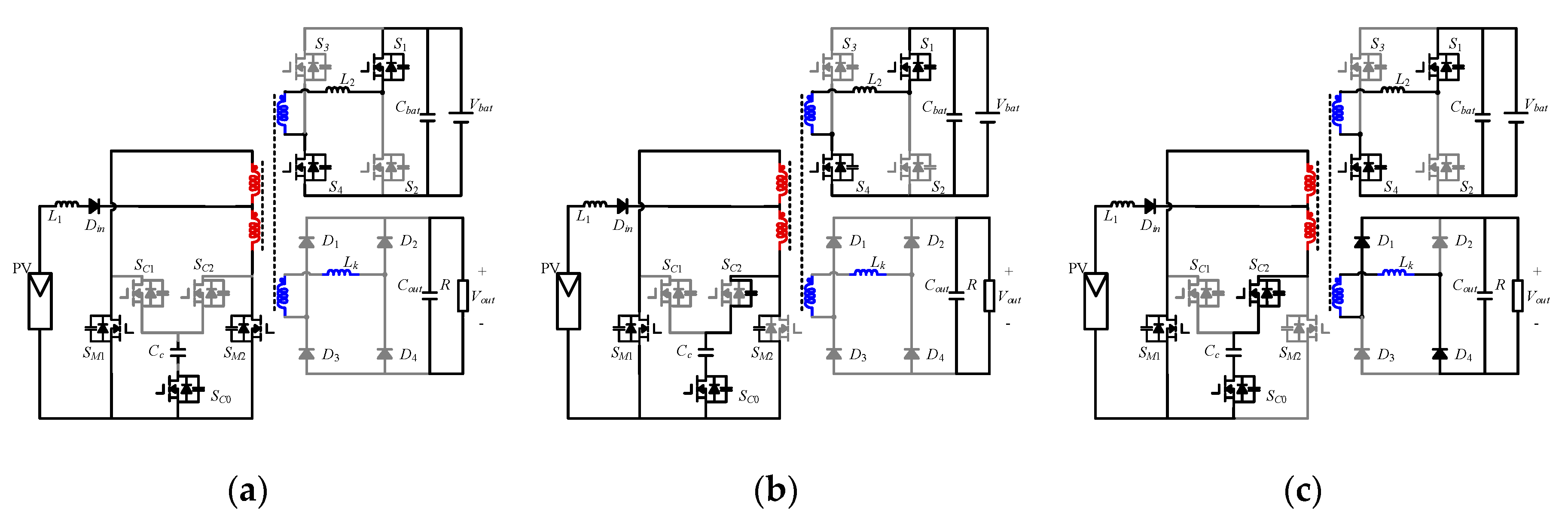
2. Analysis of the Basic Cell

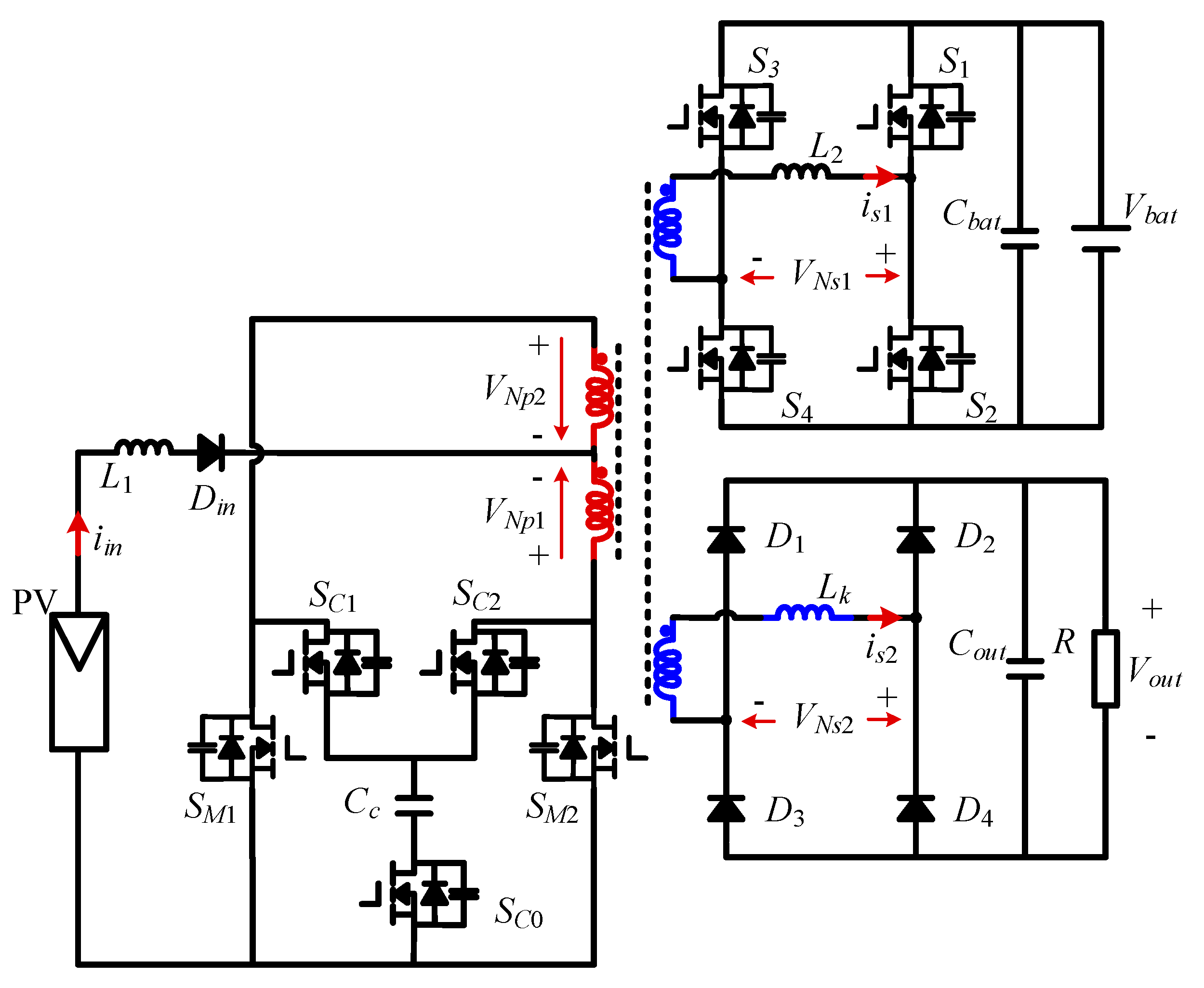
2.1. Topology of the Basic Cell

The topology of the basic power cell with PV panel is shown in Figure 2, consisting of the primary circuit, the battery side circuit, and the single-phase bridge rectifier linked through a transformer with four windings. The components in the primary circuit contains two main switches SM1SM2, three clamp switches SC0SC1, one clamp capacitor Cc, one input inductor L1, and one input diode Din. The battery side circuit is formed by two phase legs consisting of switches S1, S4 and S2, S3, and the inductor L2. The output is in series connection with the single-phase bridge rectifier consisting of four diodes D1D4. The transformer has the turns ratio as Np1:Np2:Ns1:Ns2 = 1:1:1:n, and the leakage inductance connected with the output side is Lk.

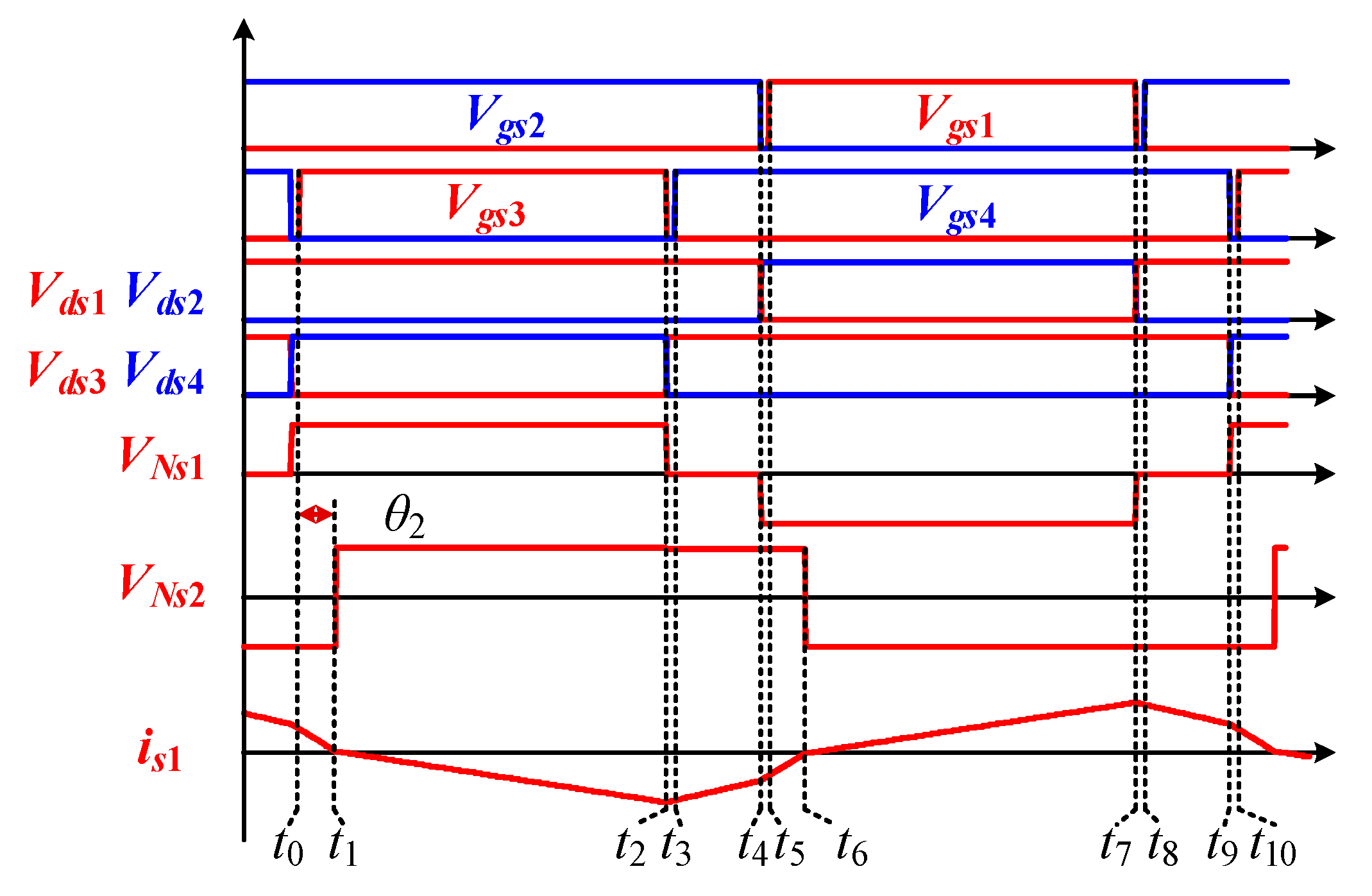
2.2. Operation of the Basic Cell with PV Source

The equivalent circuits of different operation modes and the steady-state waveforms for the basic cell with PV source are illustrated in Figure 3 and Figure 4. VgsM1VgsM2 are the control signals with the duty cycle Dp for the two main switches SM1SM2, which have a 180° phase shift angle. Vgsc1Vgsc2 are the control signals for the two clamp switches SC1SC2, which are complementary to VgsM1VgsM2, respectively. Vgs1Vgs4 are the control signals for switches S1S4, which are set as Vgs1 = Vgs4, and Vgs2 = Vgs3. Vgs1 and Vgs3 have the same duty cycle Db. VdsM1VdsM2, Vdsc1Vdsc2, and Vds1Vds4 are the drain–source voltages of switches SM1SM2, SC1SC2, and S1S4. When there is the PV source, the switch SC0 is on permanently and Db = 0.5. The PWM control for CFPP and the phase shift angle θ1 between the VCFPP and VFB regulates the voltage level and power of the battery and output. To simplify the analysis, all switches and diodes are assumed to be identical, and the clamp capacitor is large enough so that the voltage ripple can be ignored.
In this example, the battery is charged. Only the operation of the basic cell during t0t6 is introduced in this part because of the symmetrical operation.
Mode 1 (t0~t1): In this mode, the main switches SM1 and SM2 are on. The primary sides Np1, Np2 are short-circuited. All the four diodes are reverse biased. At the same time, S1 and S4 are on. The voltage of the battery side Ns1 is negative.
Mode 2 (t1~t2): At t1, the main switch SM2 is turned off. The primary-side referred inductance resonates with the parasitic capacitances of SM2 and SC2. The voltage across SC2 drops to zero at t3 so that ZVS turn-on of SC2 is obtained.
Mode 3 (t2~t3): At t2, the clamping switch SC2 is turned on with zero voltage. The energy is transferred from the PV and input inductor L1 to the output. The diodes D1 and D3 are forward biased, and the current is increases.
Mode 4 (t3~t4): At t3, switches S1 and S4 are turned off. The voltage VFB becomes positive. The inductor L2 resonates with the parasitic capacitances of S1S4. The voltage across S2 and S3 drops to zero at t5 so that ZVS turn-on of S2 and S3 is obtained.
Mode 5 (t4~t5): At t4, switches S2 and S3 are turned on with zero-voltage. The power starts to be delivered into the FB circuit.
Mode 6 (t5~t6): At t5, the clamp switch SC2 is turned off. The primary-side referred inductance resonates with the parasitic capacitances of SM2 and SC2. The voltage across SM2 drops to zero at t6 so that ZVS turn-on of SM2 is obtained.
Altering the duty cycle Dp, the three-level voltage waveforms VNp1,2 and VNs2 are generated in the primary side and the rectifier bridge. According to the flux balance of the input inductor L1, the clamp voltage can be derived as
V i n ( D p 0.5 ) + ( V i n 0.5 V C c ) ( 1 D p ) = 0
V C c = V i n ( 1 D p )
The output voltage can be determined as
V o u t n V o u t D p n V i n + V i n D p V i n D p + V i n 2 = 0
V o u t = n 2 V i n ( 1 D p )
Additionally, based on the average power flow calculation of bidirectional power converters [30,31], the power transfer between Pin and Pbat with the switching frequency fs is obtained in Equation (5). A specific phase shift θ1 controls the power delivered to the battery. When 0 < θ1 < π, the power can be transferred from the PV to battery and vice versa. Additionally, the power transfer between Pin and Pbat with the switching frequency fs is obtained as
P i n b a t = 1 T 0 T v p ( t ) i L ( t ) = V i n V b a t ω L 2 ( 2 ( 1 D p ) θ 1 θ 1 2 π 2 ( 1 D p ) 2 π + ( 1 D p ) π ) D p 0.5
where ω = 2πfs.

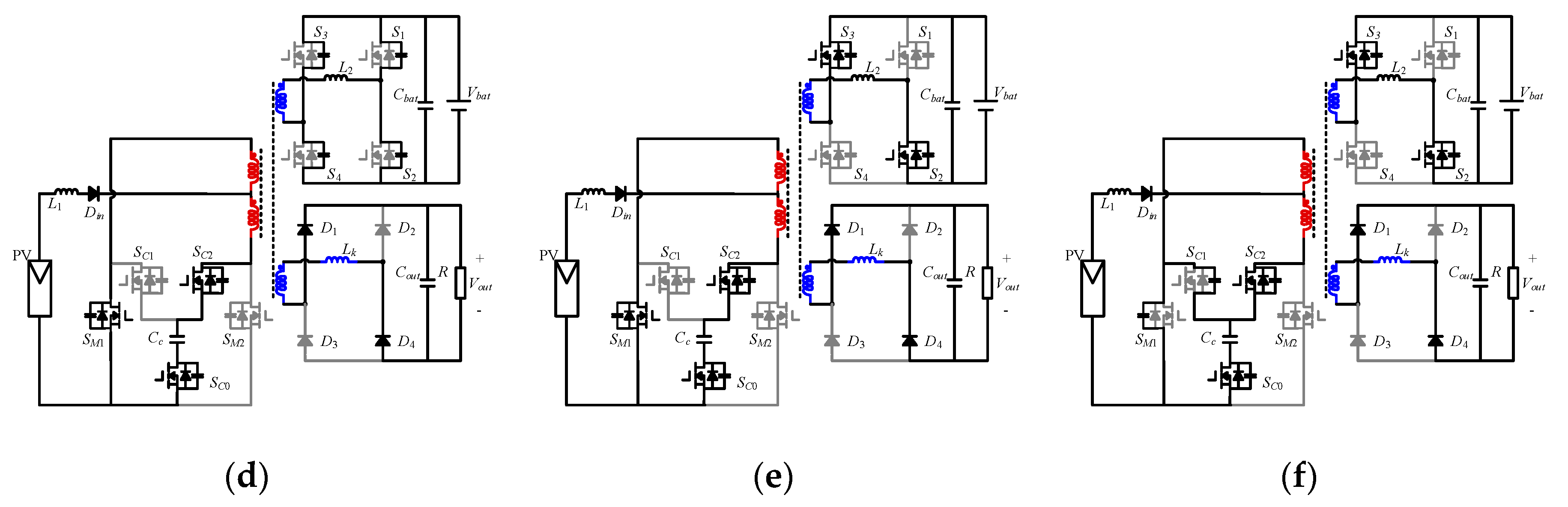
2.3. Operation of the Basic Cell without PV Source

When there is no PV source, the equivalent circuits of different modes and the steady-state waveforms for the basic cell are illustrated in Figure 5 and Figure 6. Vgs1 and Vgs3 have a 180° phase shift angle with the duty cycle Db ≤ 0.5. Vgs2, Vgs4 are complementary to Vgs1, Vgs3 respectively. Additionally, the primary circuits are blocked to reduce the conduction losses. Because the operation is symmetrical, only the operation during t0t5 is introduced in this part.
Mode 1 (t0t1): At t0, switch S3 is turned on. There is a phase shift θ2 between VNs1 and VNs2, which is dependent on the inductance L2, Lk and the output load. The battery-side current is1 recovers to zero at t1. The current is1 as a function of β = ωt is derived as
i ( β ) = ( V b a t + V o ω L b a t ) β + i ( 0 )
where Vo is the battery-side referred output voltage, which equals to Vout/n; L′bat is the battery-side referred inductance and L′bat = L2 + Lout/n2.
Mode 2 (t1t2): At t2, is1 starts to decrease. The voltage of VNs2 becomes positive. In this mode, is1 is determined as
i ( β ) = ( V b a t V o ω L b a t ) ( β θ 2 ) + i ( θ 2 )
Mode 3 (t2t3): At t2, switch S3 is turned off. The voltage VNs1 drops to zero. The battery-side referred inductance resonates with the parasitic capacitances of switches S3 and S4. The parasitic capacitor of S4 is discharged to zero. Therefore, ZVS turn-on of S4 is obtained at t3.
Mode 4 (t3t4): At t4, switch S4 is turned on with zero voltage. The current is1 starts to increase as shown in Equation (8):
i ( β ) = ( V o ω L b a t ) ( β ( D b + t d s ) 2 π ) + i ( ( D b + t d s ) 2 π )
where tds is the dead time between switches S1S2 and S3S4.
Mode 5 (t4t5): At t4, switch S2 is turned off. The voltage VNs1 drops to negative. The battery-side referred inductance resonates with the parasitic capacitances of switches S1 and S2. The voltage across S1 is discharged to zero so that ZVS turn-on of S1 can be achieved at t5.
Because the dead time tds is relatively short, modes 3, 5 can be neglected in the calculation and the phase shift between voltage VNs1 and VNs2 defined as θ2. Therefore, Equation (9) is derived according to Equation (8).
i ( β ) = ( V o ω L b a t ) ( β D b 2 π ) + i ( D b 2 π )
At t5, i(t5) = −i(t0) since it is the end of half cycle. Additionally, i(θ2) = 0. Then, θ2 can be derived as shown in Equation (10):
θ 2 = 1 2 ( D b π d π )
where d is defined as Vo′/Vbat. The power transfer is obtained as
P b a t o u t = 1 T 0 T v b a t ( t ) i s 1 ( t ) = V b a t V o u t 4 ω L b a t n ( 2 D b π π d 2 D b 2 π )

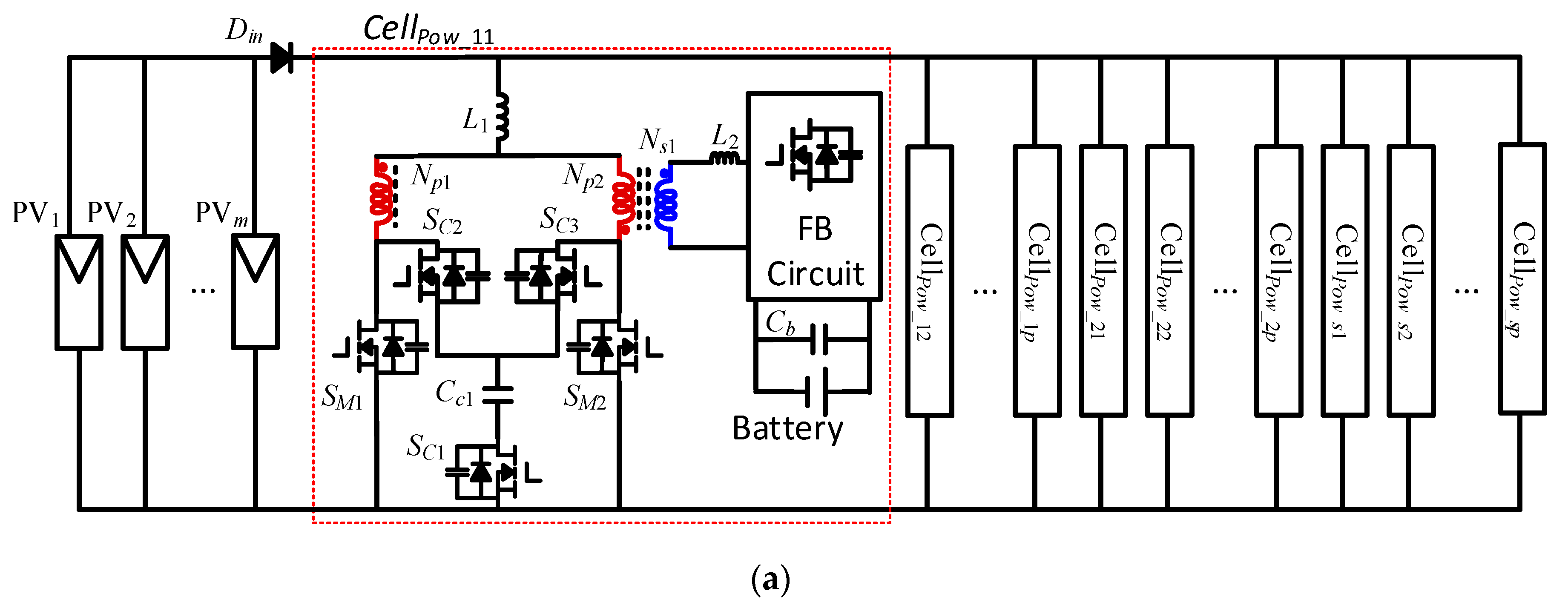
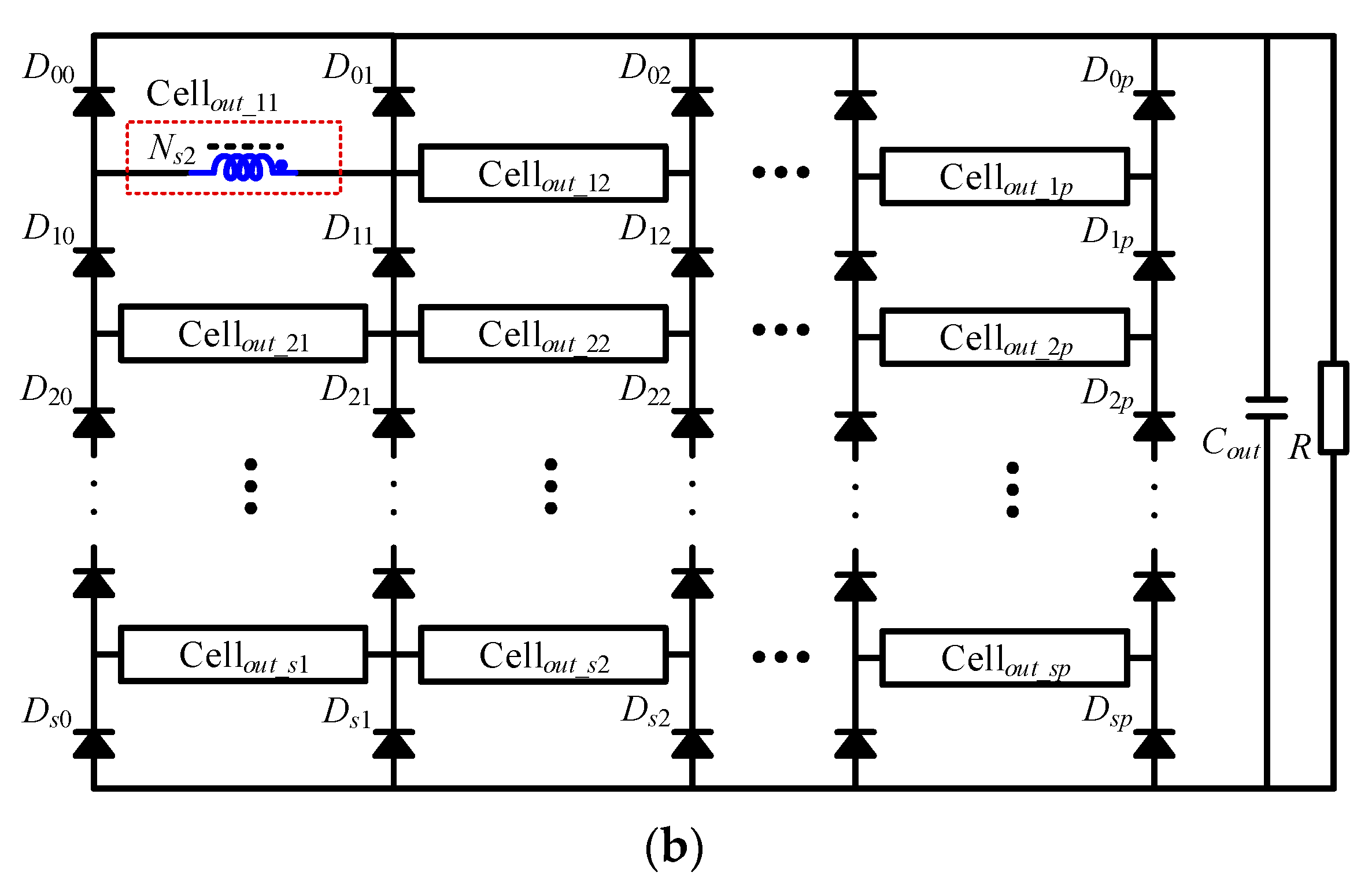
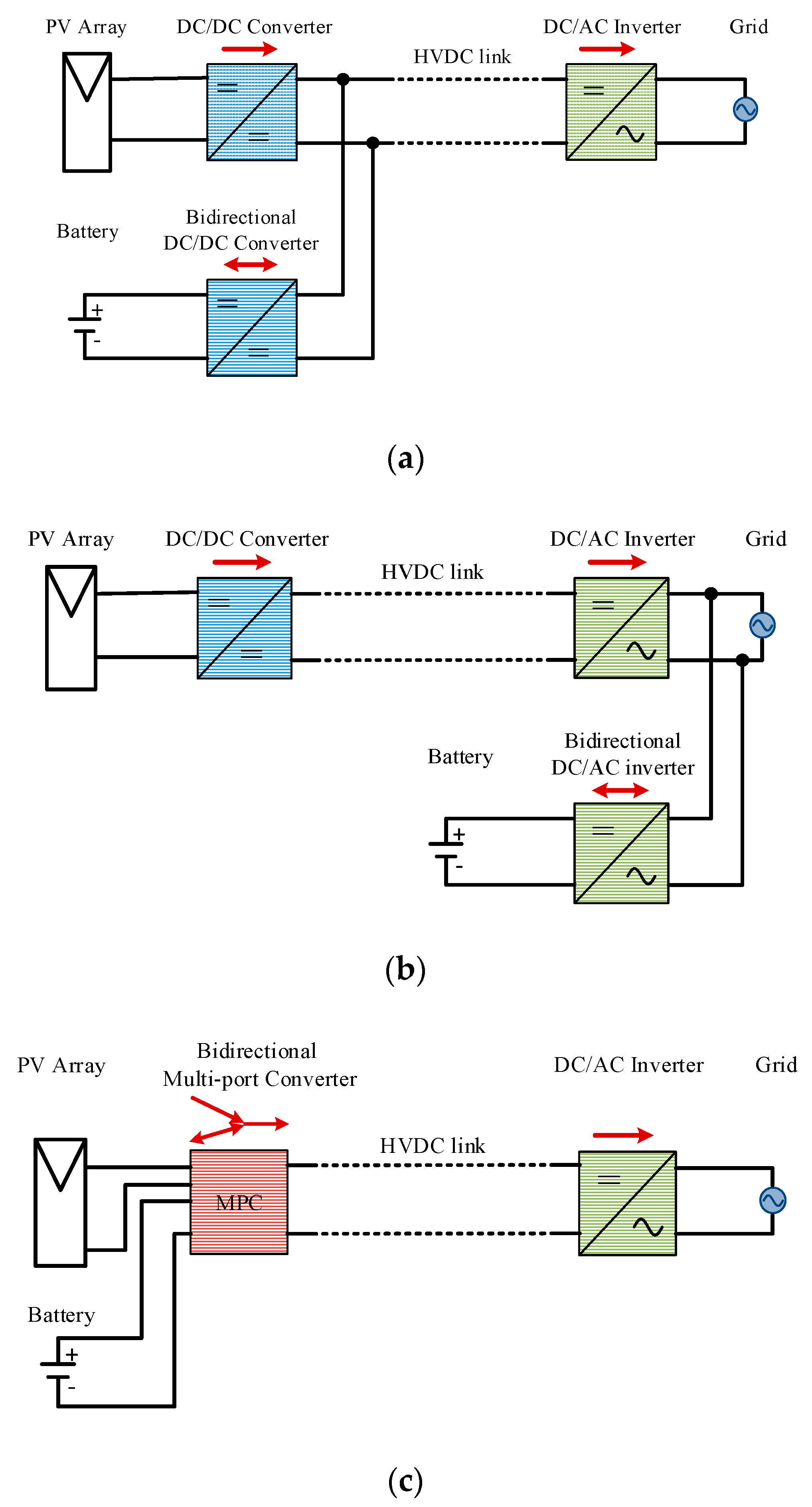
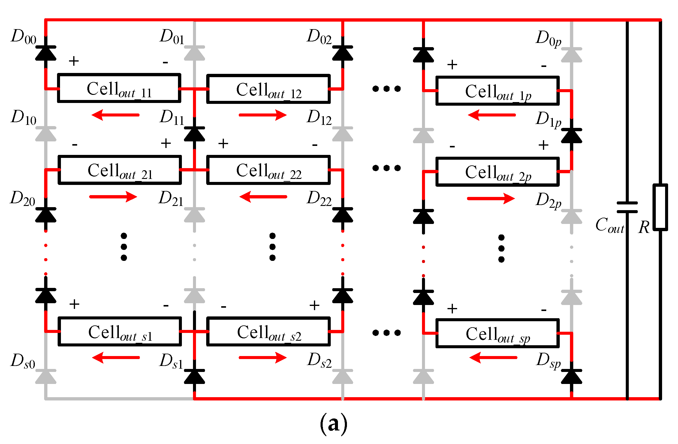
3. Analysis of the Proposed Converter with Scalable Topology

As shown in Figure 7, the proposed modular multi-port bidirectional converter is composed of the basic cell illustrated in Figure 2 The primary sides are in parallel connection with the PV source Vin. The battery cells are decentralized into each basic cell to obtain individual control. Additionally, the output-side windings Ns2 of transformers are connected in an s × p matrix configuration, where s is the row number, and p is the column number. The matrix configuration of the converter can be easily expanded to achieve high output voltage and power rating by increasing its row number and column number respectively. Therefore, the converter can satisfy the RESs applications demanding high voltage step-up ratios and high power scales.

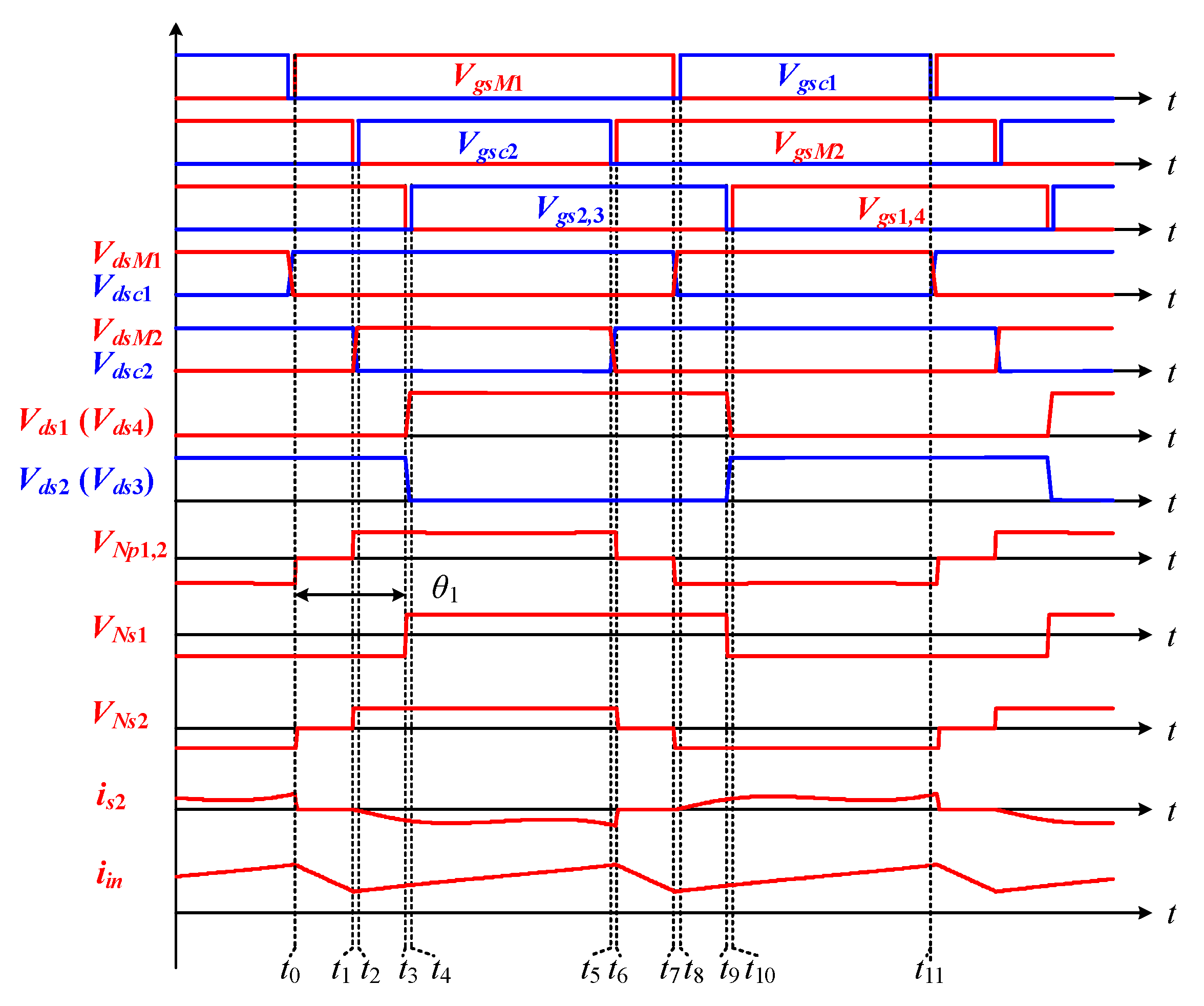
3.1. Operation Principle of the Scalable Topology
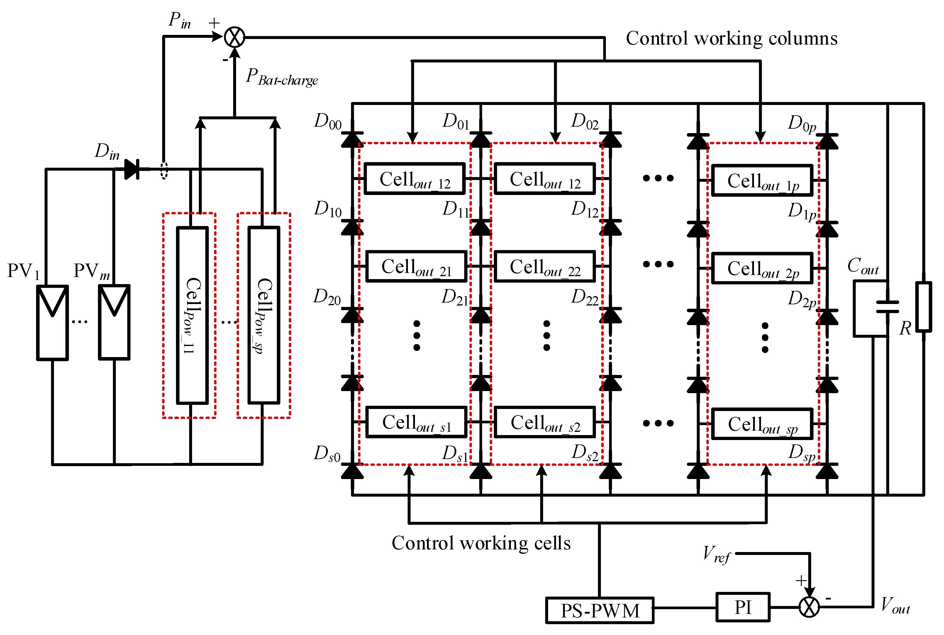
Cells of the scalable topology have similar operations with those for one basic cell except that the drive signals of switches in adjacent cells have a 180° phase shift. For example, cells 12, 21, 23, and 32 have the same drive signals, whose phases are shifted by 180° from the corresponding drive signals of cell 22. Hence, the polarities of output voltages Vs2 and currents is2 for adjacent cells are opposite. Then, the column interleaved working strategy of matrix topology is shown in Figure 8.
The output voltage is the sum of the voltages Vs2 of cells in the same column, and the output current is the sum of the currents is2 in every column, which are shown in Equation (12) with the assumption that every cell has the identical output voltage and current. Therefore, the high output voltage and power rating can be easily obtained by increasing the row and column number of the matrix topology.
{ V o , s × p = s × V s 2 = s × n 2 ( 1 D p ) V i n I o , s × p = p × I s 2
Due to the parallel connection of primary-side circuit and individual battery-side circuit, all switches have the low voltage rating with high output voltage. The voltage ratings of switches in basic cells are derived as shown in Equation (13).
{ V d s _ N p = V C c = V i n 1 D p V d s _ N s 1 = V b a t
The current stress of diodes in columns 0 and p has half the value of Is2, which is the average output current of the basic cell. Nevertheless, the diodes in columns 1 to p − 1 have twice the current stress higher than that of other diodes, since they are connected with two basic cells. The sum of average currents of diodes in all columns equals the output current as shown in Equation (14), and the current stress of diodes is derived in Equation (15). Similarly, the voltage stress of diodes is obtained in Equation (16). For diodes in rows 1 to s − 1, the voltage stress has twice the value larger than that of the diodes in rows 0 and s.
j = 0 p I ( D i j ) = I o , s × p
I ( D i j ) = 1 2 I s 2 = { 1 2 p I o , s × p j = 0 , p 1 p I o , s × p j = 1 , 2 , , ( p 1 )
V ( D i j ) = { n 2 ( 1 D p ) V i n i = 0 , s n ( 1 D p ) V i n i = 1 , 2 , , ( s 1 )
The maximum current and voltage stress of diodes in the s × p topology are only twice larger than that of one single cell, which is much lower than the average output voltage Vo,s×p and current Io,s×p. Therefore, the low voltage/current rating semiconductor components such as switches and diodes can be used to achieve a high voltage step-up ratio and output power.

3.2. Control Scheme

Since the number of working rows determines the value of output voltage and that of working columns determines the output current, the variable output power can be obtained. As shown in Figure 9, power control is achieved by controlling the working columns according to the input current and battery charged/discharged power value. The voltage control is mandatory to meet the system operation requirements by the PS–PWM control of switches in the primary-side and battery-side circuits.

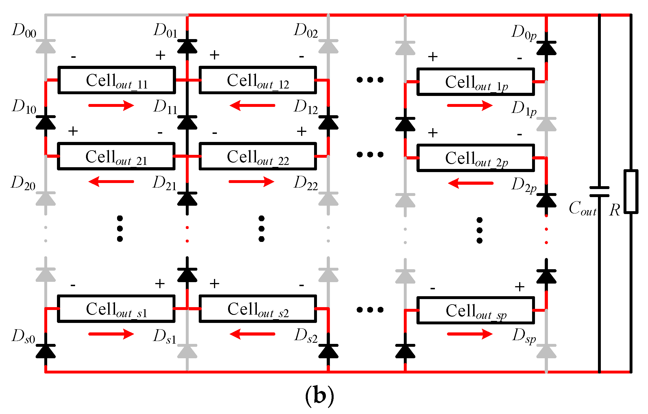
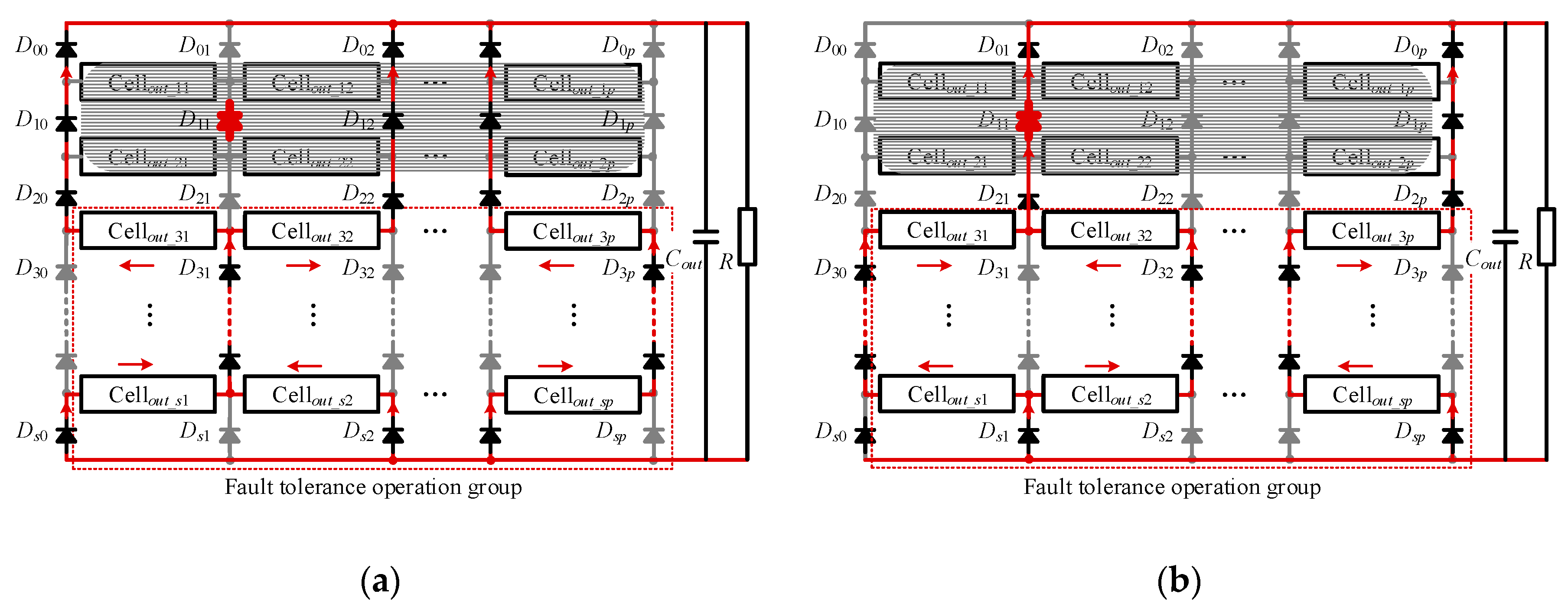
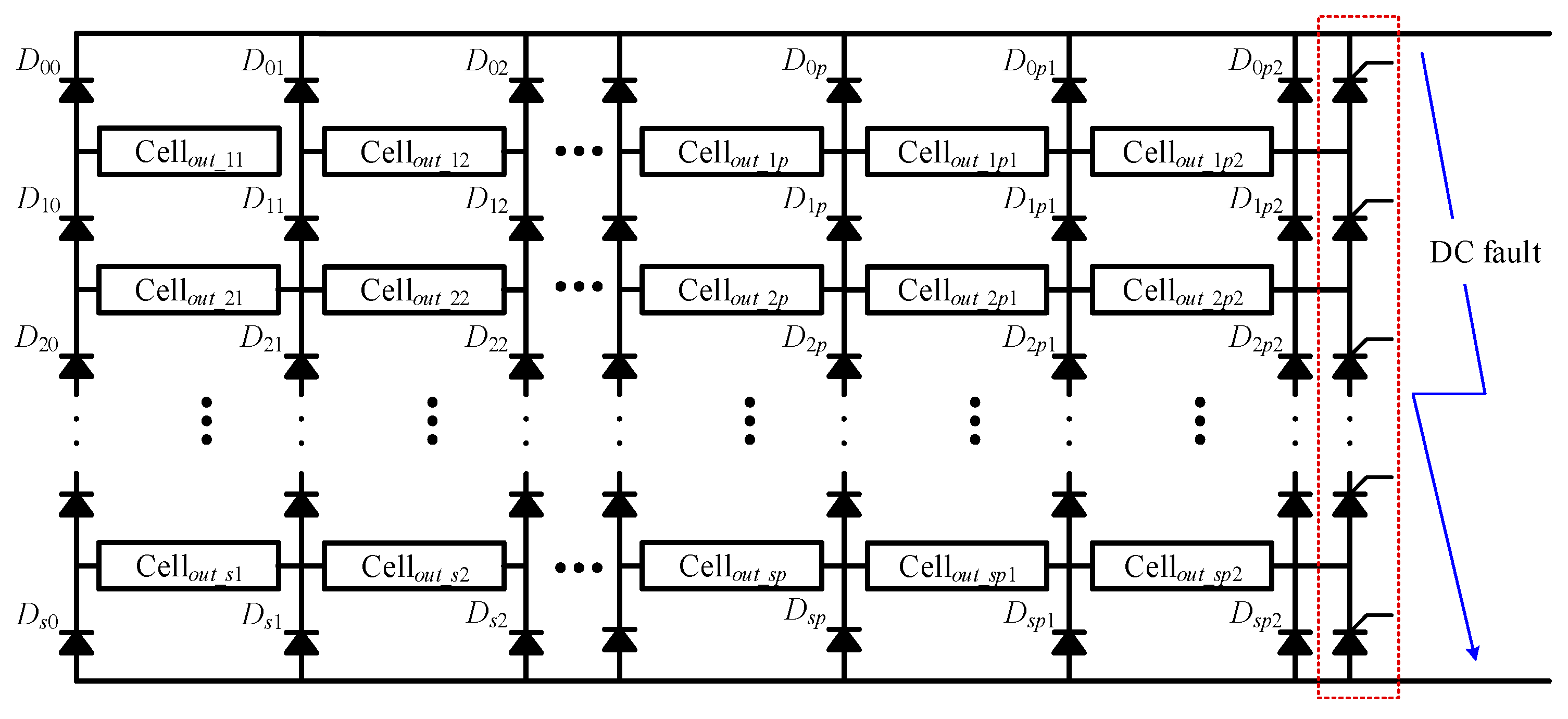
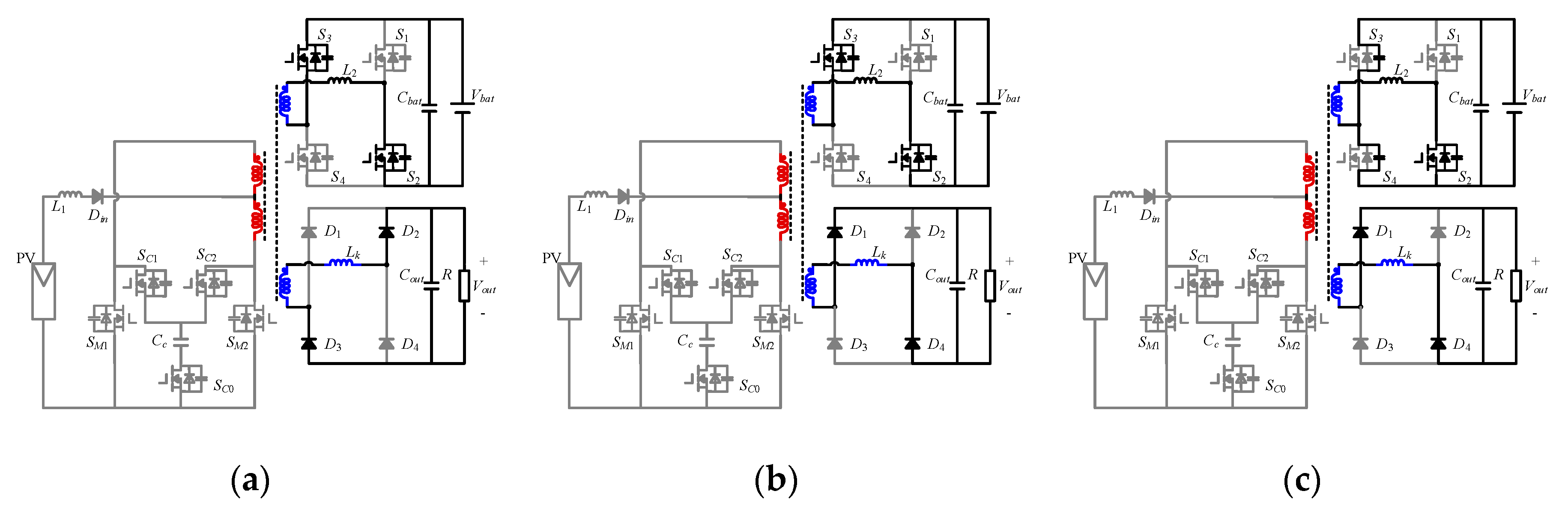
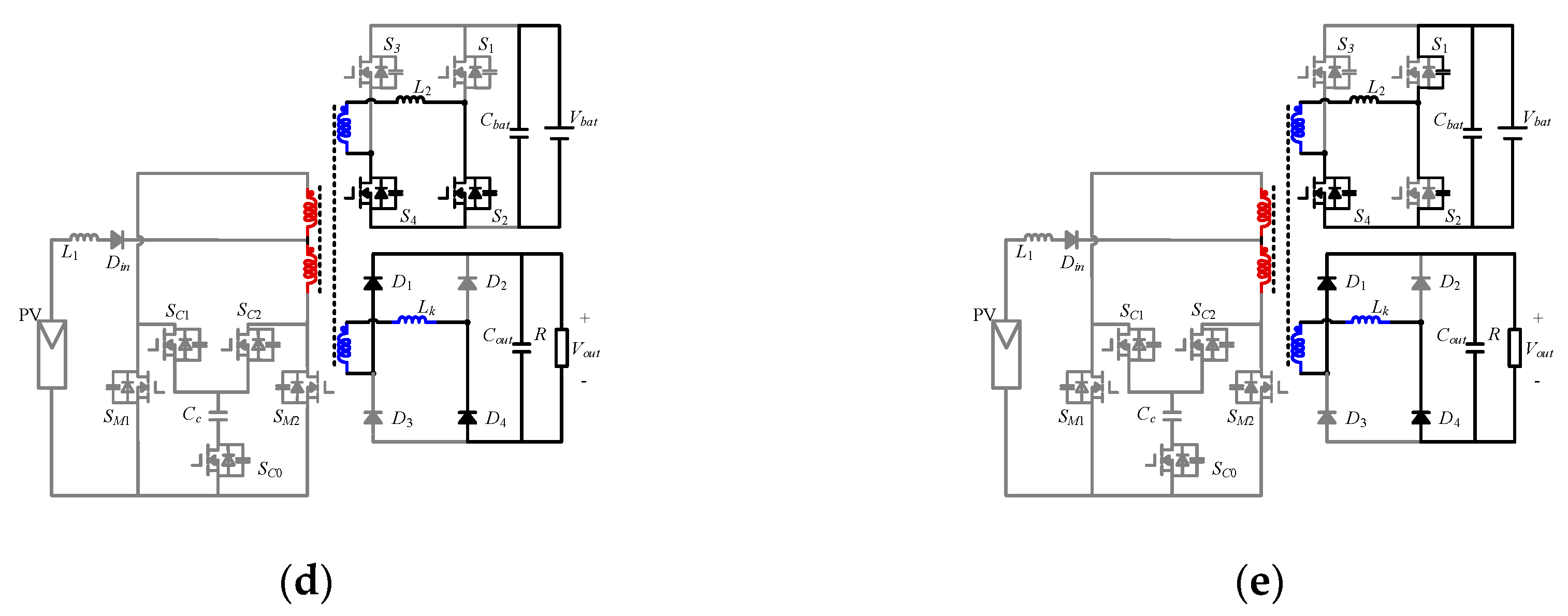
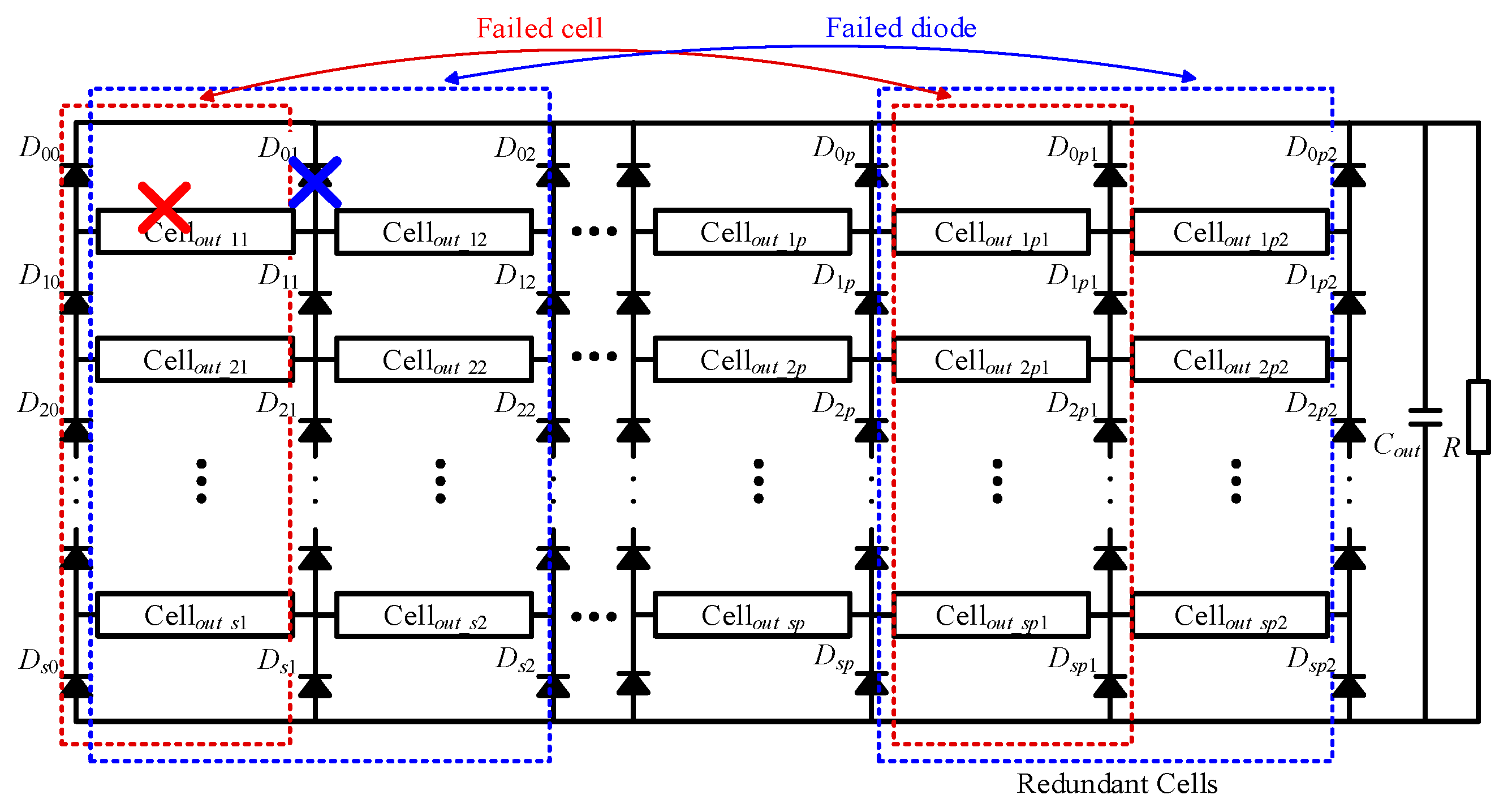
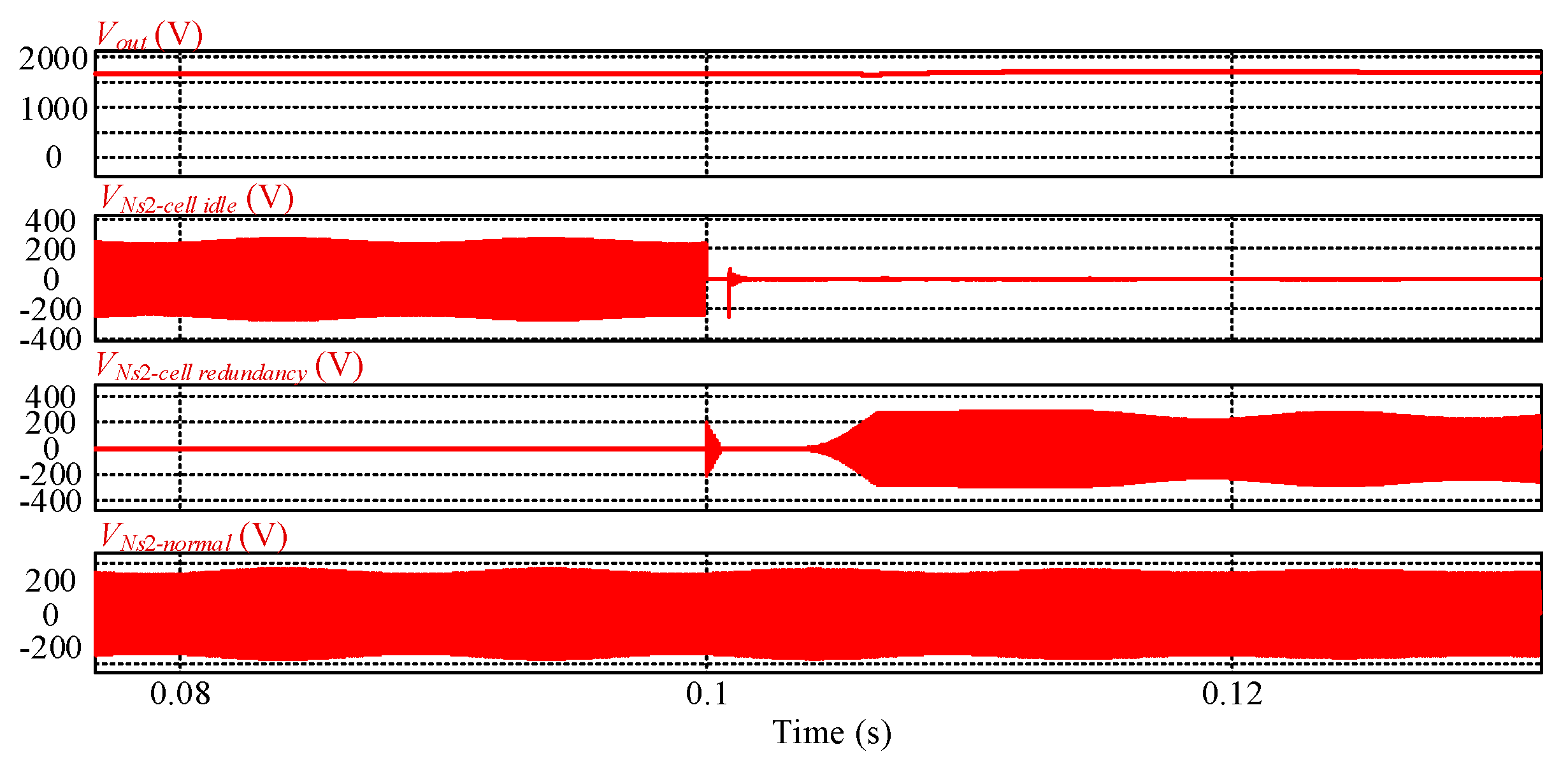
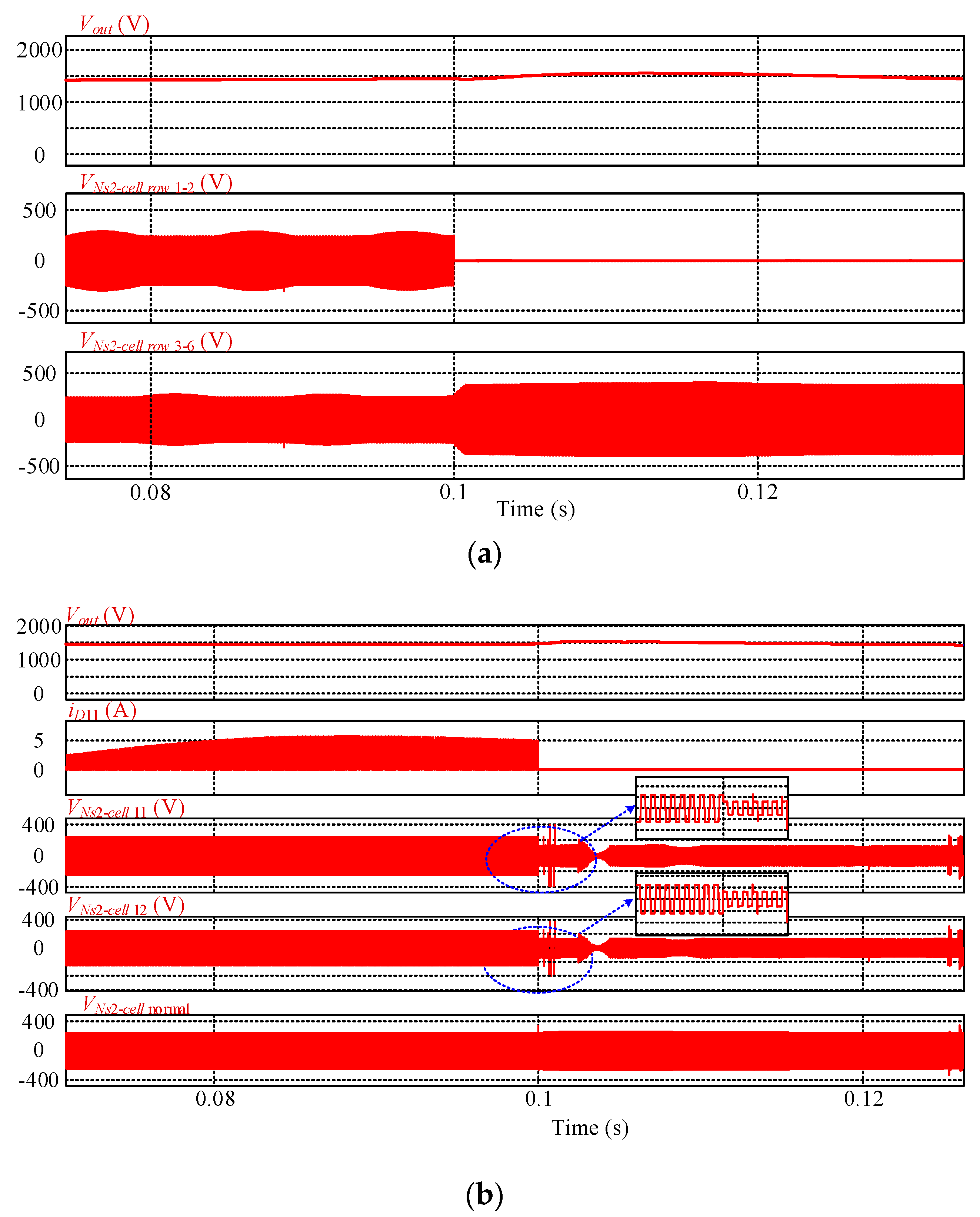
3.3. Fault Tolerance

For power electronics systems, semiconductor components are vulnerable devices [32]. With unexpectedly damaged devices, the whole system has to stop and wait for maintenance, resulting in high cost and loss. Figure 10 shows the fault tolerant operation with redundancy. In normal operation, the redundant cells in columns p1 and p2 are inactive, and the converter is working with the column interleaved strategy as shown in Figure 8. When there are failed cells, the converter can maintain normal operation by replacing the faulty column with one redundant column. For the damaged diodes in columns 1 to p − 1, two redundant columns are necessary. For example, when cell 11 fails, the column in the red dotted rectangle is replaced by the redundancy in another red dotted box. For the defective diode D11, columns 1 and 2 in the blue dotted box are idle, and the redundant columns p1 and p2 are applied.
Additionally, owing to the matrix configuration and flexible control, the converter can still obtain fault tolerance of cells and diodes without redundancy as depicted in Figure 11. When there are failed cells or short-circuited diodes, the converter can still work as in Figure 11a,b. When diode D11 is short-circuited, its connecting rows 1 and 2 are inactive to block the damaged devices. The other cells still operate with the column interleaved strategy and the duty cycle Dp of them is increased to obtain the normal output voltage with fewer working rows. The fault tolerance of the open-circuited diode can be achieved as shown in Figure 11b,c. The fault tolerance operating group consists of the adjacent columns of the failed diode D11, where the drive signals of cells in adjacent rows have a 180° phase shift and the cells in the same row have the same signals. Then, the adjacent rows have opposite polarities, and the cells in the same rows have the same polarity. Therefore, all cells in the faulty group are connected in series to block the damaged diode. To achieve the same terminal voltage, the output voltages of cells in the faulty group is half of that in the normal operation groups since the number of cells series-connected in the faulty group is twice larger than that in the normal operation group.
Furthermore, as illustrated in Figure 12, the diodes in the secondary circuits can be prevented from damage under DC fault condition, which is similar to the MMC converter by adding thyristors because they have a higher I2t capacity compared with diodes.

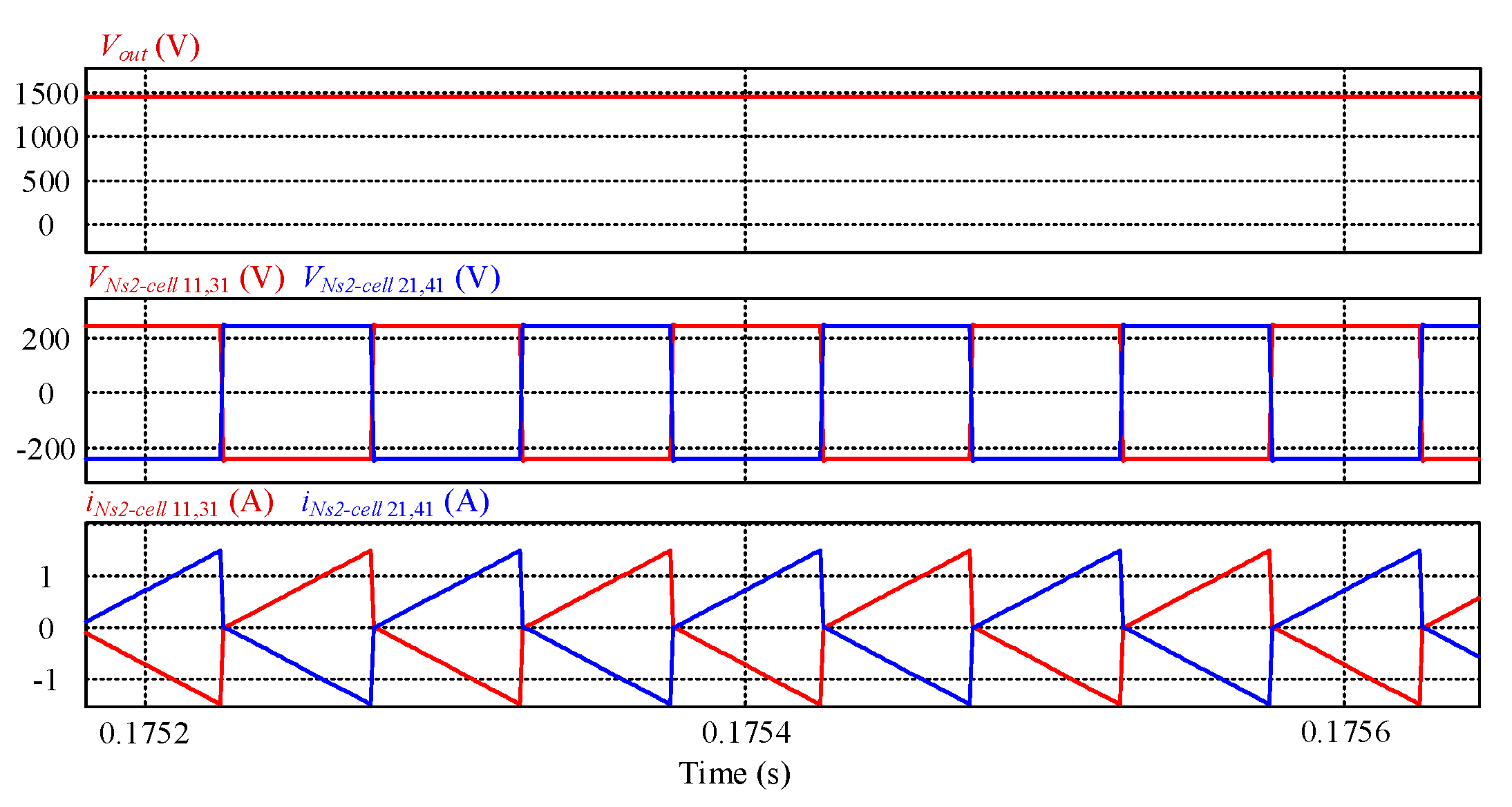
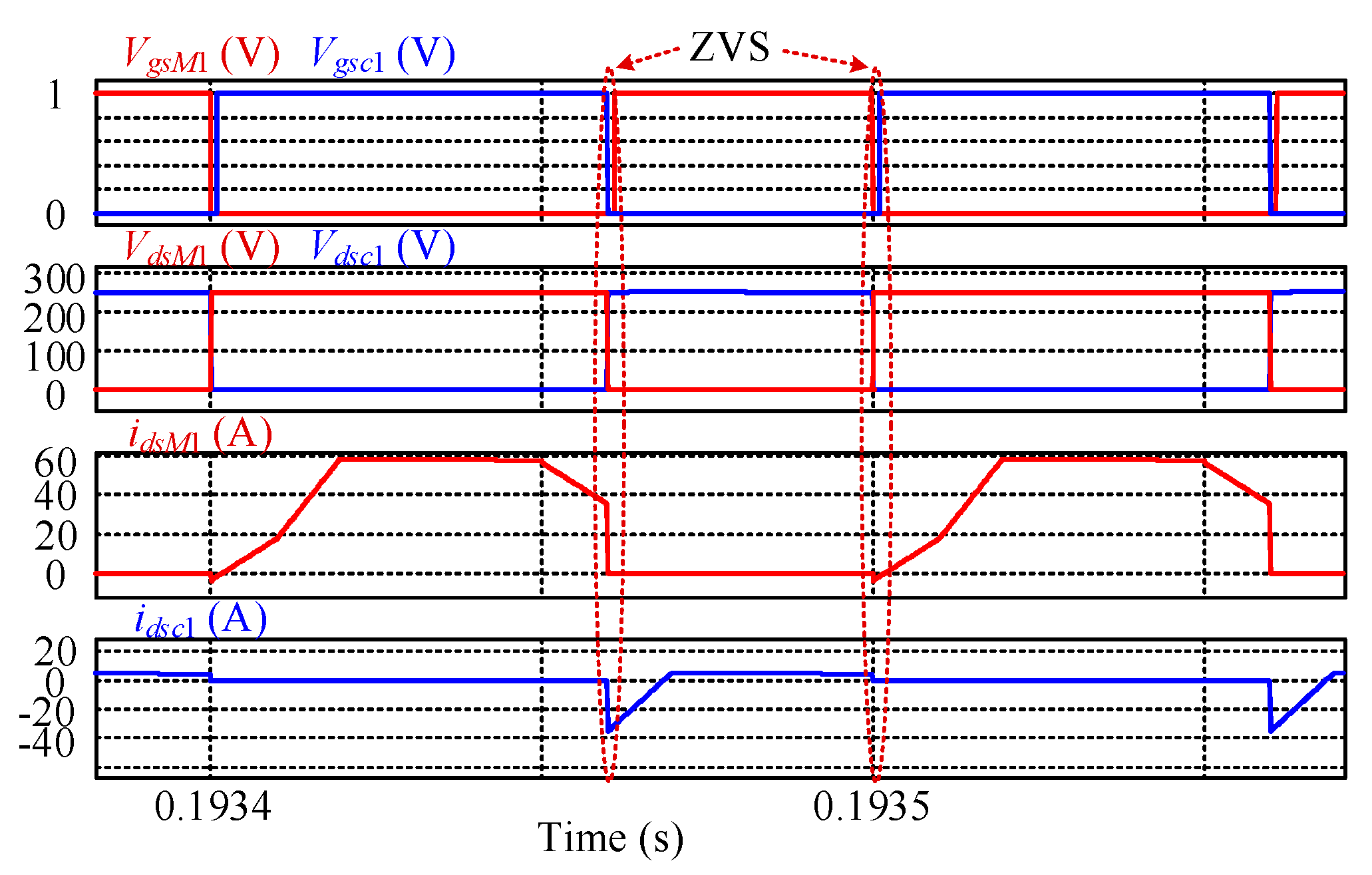
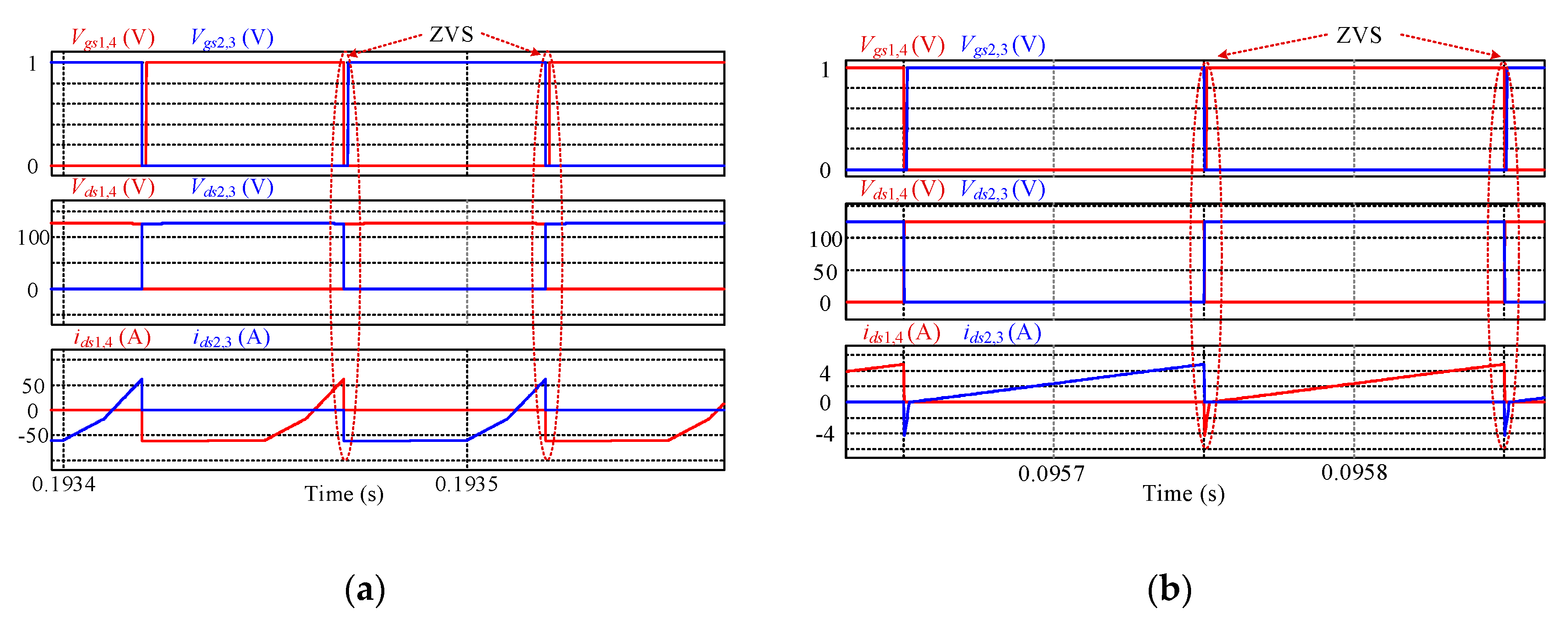
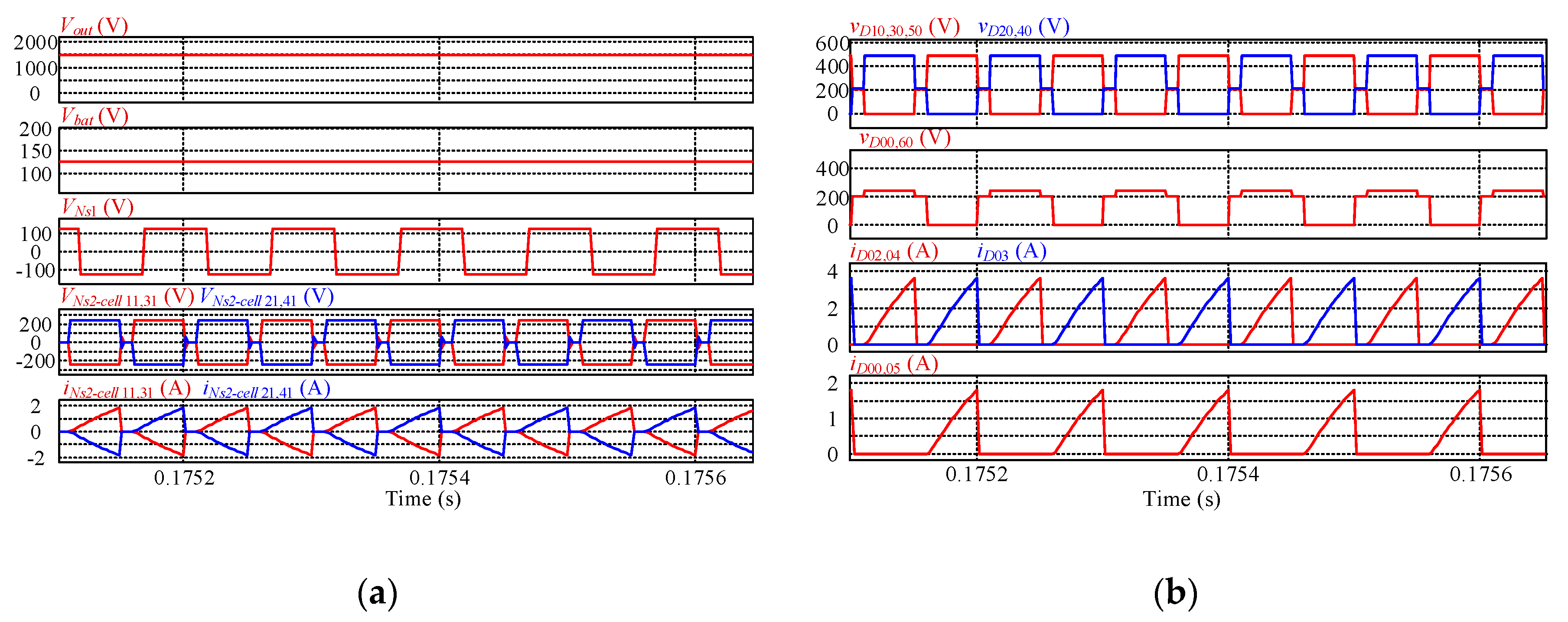
4. Simulation Results and Discussion

To verify the functionality of the proposed converter, a simulation model consisting of six rows×six columns that is similar to the one shown in Figure 7 is built in the software PSIM. For the six columns, columns 1–4 are active, while columns 5–6 are redundant. Table 1 presents the simulation parameters
The steady-state waveforms of the converter are shown in Figure 13 and Figure 14. All cells in columns 1–4 work with the column interleaved strategy. The adjacent cells have the opposite voltage and current polarities. With six rows in the matrix structure, the power switches have low voltage stress, which is 1/6 of the output voltage, and the voltage and current ratings of all diodes are as low as 1/6 or 1/3 of the output voltage and current respectively.
As illustrated in Figure 15, before turning on switch SM1 or SC1 in the primary circuits, the drain-source currents of both switches, idsM1 and idsC1, are negative which shows the currents flow through their parasitic diodes so that zero-voltage turn-on is achieved for SM1 or SC1. Similarly, the switches SM2 and SC2 can also obtain ZVS due to symmetrical operation.
The voltage–current waveforms for switches S1S4 are depicted in Figure 16 where Db is set as 0.5. As shown in Figure 16a, when the battery is charged, the currents flow through the parasitic diodes of the corresponding switch before the switch is turned on so that ZVS is achieved. When the battery is discharged in Figure 16b, four switches still can be turned on with zero voltage due to the resonance between the inductance L2 and the parasitic capacitance of switches. Therefore, all switches can achieve ZVS turn-on, which significantly reduces the switching loss.
Figure 17 illustrates the fault tolerance capability with redundancy. At 0.1 s, columns 1–2 are inactive in the case that there are fault cells in columns 1–2 or diodes in columns 0–1. Then the redundant columns 5–4 start to work to guarantee the normal operation.
Figure 18 presents the fault tolerance operation without redundancy, where only columns 1–4 are active. In Figure 18a, when diode D11 is short-circuited, the cells in rows 1–2 are inactive at 0.1 s to block the defective component. The duty cycle of switches in primary circuits is modified according to Equation (9) to maintain the normal output voltage. In Figure 18b, diode D11 is open-circuited at 0.1 s. To block the failed components, the cells in the columns adjacent to D11 are all in series-connection by changing the voltage polarities of the cells in column 1. Furthermore, the voltages of cells in the faulty group are reduced to half of that in the normal operation group to obtain the same terminal voltage.

5. Conclusions

A modular multi-port bidirectional high power level DC/DC power converter applied for HVDC transmission of RESs is proposed in this paper. Thanks to the three-port basic cell, ES can be integrated with HVDC system with low component count as well as high compactness, and the power is transferred within one conversion stage. Additionally, due to the modularity, the proposed converter can achieve high output voltage and power by adding SMs.
The performances of isolated MPCs, partial-isolated MPCs, MMCs with ES system, and the proposed converter are compared. The proposed model appears to be more efficient and reliable, presenting the features of low switching loss, high DC voltage conversion ratio, high control flexibility, and high reliability.
The simulation results verify the advantages of the proposed converter such as the low voltage and current ratings of semiconductor components, ZVS turn-on of power switches, flexible control and improved fault tolerance operation.

Author Contributions

Conceptualization, Y.H.; Formal analysis, S.S. and Y.H.; Investigation, S.S.; Methodology, S.S. and Y.H.; Software, S.S.; Supervision, Y.H.; Validation, S.S.; Writing—original draft, S.S.; Writing—review and editing, W.L., K.N., H.X., and J.S.

Funding

This research received no external funding.

Conflicts of Interest

The authors declare no conflict of interest.

References

  1. LLas, A.; Ralon, P.; Rodriguez, A.; Taylor, M. Renewable Power Generation Costs in 2017; International Renewable Energy Agency (IRENA): Abu Dhabi, UAE, 2018. [Google Scholar]
  2. Integrating Renewable Electricity on the Grid; A Report by the APS Panel on Public Affairs; APS: Washington, DC, USA, 2011.
  3. Al-Absi, M.; Khalifa, Z.; Hussein, A. A new capacitor-less buck DC-DC converter for LED applications. Act. Passiv. Electron. Compon. 2017, 2017, 2365848. [Google Scholar] [CrossRef]
  4. Sun, J.; Li, M.; Zhang, Z.; Xu, T.; He, J.; Wang, H.; Li, G. Renewable energy transmission by HVDC across the continent: System challenges and opportunities. CSEE J. Power Energy Syst. 2017, 3, 353–364. [Google Scholar] [CrossRef]
  5. Oni, O.E.; Davidson, I.E.; Mbangula, K.N. A review of LCC-HVDC and VSC-HVDC technologies and applications. In Proceedings of the 2016 IEEE 16th International Conference on Environment and Electrical Engineering (EEEIC), Florence, Italy, 7–10 June 2016; pp. 1–7. [Google Scholar]
  6. Oates, C. Modular multilevel converter design for VSC HVDC applications. IEEE J. Emerg. Sel. Top. Power Electron. 2015, 3, 505–515. [Google Scholar] [CrossRef]
  7. Singh, H.; Vadhera, S. Performance enhancement of VSC-HVDC system using energy storage device. In Proceedings of the 2015 International Conference on Energy, Power and Environment: Towards Sustainable Growth (ICEPE), Shillong, India, 12–13 June 2015; pp. 1–6. [Google Scholar]
  8. Riffonneau, Y.; Bacha, S.; Barruel, F.; Ploix, S. Optimal power flow management for grid connected PV systems with batteries. IEEE Trans. Sustain. Energy 2011, 2, 309–320. [Google Scholar] [CrossRef]
  9. Chiang, S.-J.; Chang, K.; Yen, C. Residential photovoltaic energy storage system. IEEE Trans. Ind. Electron. 1998, 45, 385–394. [Google Scholar] [CrossRef]
  10. Nakayama, H.; Hiraki, E.; Tanaka, T.; Koda, N.; Takahashi, N.; Noda, S. Stand-alone photovoltaic generation system with combined storage using lead battery and EDLC. In Proceedings of the 13th International Power Electronics and Motion Control Conference, EPE-PEMC 2008, Poznan, Poland, 1–3 September 2008; pp. 1877–1883. [Google Scholar]
  11. Sayed, S.; Elmenshawy, M.; Elmenshawy, M.; Ben-Brahim, L.; Massoud, A. Design and analysis of high-gain medium-voltage DC-DC converters for high-power PV applications. In Proceedings of the 2018 IEEE 12th International Conference on Compatibility, Power Electronics and Power Engineering (CPE-POWERENG), Doha, Qatar, 10–12 April 2018; pp. 1–5. [Google Scholar]
  12. Haque, M.M.; Wolfs, P.; Alahakoon, S. Dual active bridge and matrix converter based three-port converter topology for grid interactive PV-battery system. In Proceedings of the 2017 Australasian Universities Power Engineering Conference (AUPEC), Melbourne, VIC, Australia, 19–22 November 2017; pp. 1–6. [Google Scholar]
  13. Xiangjiaba-Shanghai, The World’s Most Powerful and Longest ultra High Voltage Direct Current Project to Go into Commercial Operation, in July 2010. Available online: https://new.abb.com/systems/hvdc/references/xiangjiaba---shanghai (accessed on 10 August 2018).
  14. Tao, H.; Kotsopoulos, A.; Duarte, J.L.; Hendrix, M.A. Transformer-coupled multiport ZVS bidirectional DC-DC converter with wide input range. IEEE Trans. Power Electron. 2008, 23, 771–781. [Google Scholar] [CrossRef]
  15. Krishnaswami, H.; Mohan, N. Three-port series-resonant DC-DC converter to interface renewable energy sources with bidirectional load and energy storage ports. IEEE Trans. Power Electron. 2009, 24, 2289–2297. [Google Scholar] [CrossRef]
  16. Jakka, V.N.S.R.; Shukla, A.; Demetriades, G.D. Dual-transformer-based asymmetrical triple-port active bridge (DT-ATAB) isolated DC-DC converter. IEEE Trans. Ind. Electron. 2017, 64, 4549–4560. [Google Scholar] [CrossRef]
  17. Asa, E.; Colak, K.; Bojarski, M.; Czarkowski, D. Asymmetrical duty-cycle and phase-shift control of a novel multiport CLL resonant converter. IEEE J. Emerg. Sel. Top. Power Electron. 2015, 3, 1122–1131. [Google Scholar] [CrossRef]
  18. Yi, F.; Cai, W. Modeling, control, and seamless transition of the bidirectional battery-driven switched reluctance motor/generator drive based on integrated multiport power converter for electric vehicle applications. IEEE Trans. Power Electron. 2016, 31, 7099–7111. [Google Scholar]
  19. Jabbari, M.; Dorcheh, M.S. Resonant multi-input/multi-output/bidirectional ZCS step-down DC-DC converter with systematic synthesis for point-to-point power routing. IEEE Trans. Power Electron. 2018, 33, 6024–6032. [Google Scholar] [CrossRef]
  20. Vel, C.S.; Venkatesan, T. Analysis of non-isolated multi-port single ended primary inductor converter or standalone applications. Energies 2018, 11, 539. [Google Scholar] [CrossRef]
  21. Wu, H.; Xu, P.; Hu, H.; Zhou, Z.; Xing, Y. Multiport converters based on integration of full-bridge and bidirectional DC-DC topologies for renewable generation systems. IEEE Trans. Ind. Electron. 2014, 61, 856–869. [Google Scholar] [CrossRef]
  22. Ding, Z.; Yang, C.; Zhang, Z.; Wang, C.; Xie, S. A novel soft-switching multiport bidirectional DC-DC converter for hybrid energy storage system. IEEE Trans. Power Electron. 2014, 29, 1595–1609. [Google Scholar] [CrossRef]
  23. Hu, Y.; Xiao, W.; Cao, W.; Ji, B.; Morrow, D.J. Three-port DC-DC converter for stand-alone photovoltaic systems. IEEE Trans. Power Electron. 2015, 30, 3068–3076. [Google Scholar] [CrossRef]
  24. Uno, M.; Oyama, R.; Sugiyama, K. Partially-isolated single-magnetic multi-port converter based on integration of series-resonant converter and bidirectional PWM converter. IEEE Trans. Power Electron. 2018, 33, 9575–9587. [Google Scholar] [CrossRef]
  25. Wersland, S.B.; Acharya, A.B.; Norum, L.E. Integrating battery into mmc submodule using passive technique. In Proceedings of the 2017 IEEE 18th Workshop on Control and Modeling for Power Electronics (COMPEL), Stanford, CA, USA, 9–12 July 2017; pp. 1–7. [Google Scholar]
  26. Henke, G.; Bakran, M.-M. Balancing of modular multilevel converters with unbalanced integration of energy storage devices. In Proceedings of the 2016 18th European Conference on Power Electronics and Applications (EPE’16 ECCE Europe), Karlsruhe, Germany, 5–9 September 2016; pp. 1–10. [Google Scholar]
  27. Li, N.; Gao, F.; Hao, T.; Ma, Z.; Zhang, C. SOH balancing control method for the MMC battery energy storage system. IEEE Trans. Power Electron. 2018, 65, 6581–6591. [Google Scholar] [CrossRef]
  28. Song, S.; Hu, Y.; Ni, K.; Yan, J.; Chen, G.; Wen, H.; Ye, X. Multi-port high voltage gain modular power converter for offshore wind farms. Sustainability 2018, 10, 2176. [Google Scholar] [CrossRef]
  29. Hu, Y.; Chen, G.; Liu, Y.; Jiang, L.; Li, P.; Finney, S.J.; Cao, W.; Chen, H. Fault-tolerant converter with a modular structure for HVDC power transmitting applications. IEEE Trans. Ind. Appl. 2017, 53, 2245–2256. [Google Scholar] [CrossRef]
  30. Li, J.; Wang, D.; Wang, W.; Jiang, J. Minimize current stress of dual-active-bridge DC-DC converters for electric vehicles based on lagrange multipliers method. Energy Procedia 2017, 105, 2733–2738. [Google Scholar] [CrossRef]
  31. De Doncker, R.W.; Divan, D.M.; Kheraluwala, M.H. A three-phase soft-switched high-power-density DC/DC converter for high-power applications. IEEE Trans. Ind. Appl. 1991, 27, 63–73. [Google Scholar] [CrossRef]
  32. Zhang, W.; Xu, D.; Enjeti, P.N.; Li, H.; Hawke, J.T.; Krishnamoorthy, H.S. Survey on fault–tolerant techniques for power electronic converters. IEEE Trans. Power Electron. 2014, 29, 6319–6331. [Google Scholar] [CrossRef]
Figure 1. Main configurations for integrating energy storage (ES) system and high voltage direct current (HVDC) system: (a) dual-converter architecture; (b) dual-inverter architecture; (c) multi-port converter architecture.
Energies 11 02711 g001
Figure 2. Topology of the basic cell.
Energies 11 02711 g002
Figure 3. Equivalent circuits of the operation modes with PV source: (a) Mode 1 (t0t1); (b) Mode 2 (t1t2); (c) Mode 3 (t2t3); (d) Mode 4 (t3t4); (e) Mode 5 (t4t5); (f) Mode 6 (t5t6).
Energies 11 02711 g003aEnergies 11 02711 g003b
Figure 4. Operating waveforms of the basic cell with PV source.
Energies 11 02711 g004
Figure 5. Equivalent circuits of the operation modes without PV source: (a) Mode 1 (t0t1); (b) Mode 2 (t1t2); (c) Mode 3 (t2t3); (d) Mode 4 (t3t4); (e) Mode 5 (t4t5).
Energies 11 02711 g005aEnergies 11 02711 g005b
Figure 6. Operating waveform of the basic cell without PV source.
Energies 11 02711 g006
Figure 7. Topology of the proposed converter with s rows and p columns: (a) primary circuits with ES system; (b) secondary circuits connecting.
Energies 11 02711 g007aEnergies 11 02711 g007b
Figure 8. Equivalent secondary circuits of the s × p topology in the column interleaved strategy: (a) column interleaved mode 1; (b) column interleaved mode 2.
Energies 11 02711 g008aEnergies 11 02711 g008b
Figure 9. Control scheme of the s × p topology.
Energies 11 02711 g009
Figure 10. Fault tolerance with redundancy.
Energies 11 02711 g010
Figure 11. Fault tolerance without redundancy: (a) Working mode 1 under diode short-circuit; (b) Working mode 2 under diode short-circuit; (c) Working mode 1 under diode open-circuit; (d) Working mode 2 under diode open-circuit.
Energies 11 02711 g011aEnergies 11 02711 g011b
Figure 12. Addition of thyristors to protect secondary diodes under DC fault.
Energies 11 02711 g012
Figure 13. Steady-state waveforms with PV source: (a) voltage/current of basic cells; (b) voltage/current of diodes.
Energies 11 02711 g013
Figure 14. Steady-state waveforms of voltage/current of basic cells without PV source.
Energies 11 02711 g014
Figure 15. Zero voltage switching (ZVS) of switches in the primary circuit.
Energies 11 02711 g015
Figure 16. Zero voltage switching (ZVS) of switches in the battery side circuit: (a) battery is charged; (b) battery is discharged.
Energies 11 02711 g016
Figure 17. Fault tolerance operation with redundancy.
Energies 11 02711 g017
Figure 18. Fault tolerance operation without redundancy: (a) Without redundancy for D11 short-circuit; (b) Without redundancy for D11 open-circuit.
Energies 11 02711 g018
Table 1. Simulation parameters.
System ParametersValuesComponentsValues
Input Voltage100 VTurns ratio 1:1:1:n1:1:1:2
Output Voltage1500 VLeakage inductance Lk60 μH
Battery125 VInput inductor L15 mH
Switching Frequency10 kHzInductor L22 mH
Output Power5 kWClamp capacitor Cc20 μF

