1. Introduction
Analog-to-digital converters (ADCs) are applied in almost all system on chip (SoC) designs as the interfaces between the analog and the digital parts. Different structures of ADCs are used for different applications. However, because of the recent design improvements made to successive approximation register (SAR) ADCs, such as resolution and the conversion rate increment, and power consumption reduction, these structures have become more popular, and they are currently widely used in circuit design. These structures are mostly composed of digital circuits and achieve high power efficiency. Binary capacitor arrays are usually applied as the digital-to-analog converter (DAC) parts in these structures. Nevertheless, as the resolution of these structures increases, the number of the capacitors in the capacitor DAC (CDAC) also increases, which makes the structure bulky [
1,
2]. In addition, the mismatch in the CDAC degrades the performance of these structures [
3,
4,
5]. To solve the mismatch issue in the CDAC, the unit capacitor sizes should be increased. Nevertheless, this approach increases the area of these structures. On the other hand, for the systems that require digitization of several signals in the system, the area problem becomes more critical, as either several ADCs or several CDACs are required in the system. Also, in such systems, for the cases where different resolutions are required, the area problem becomes more critical.
This work presents a 10- and 12-bit four–channel SAR ADC that is designed to be applied in a wireless power transfer (WPT) system. In WPT systems, there are several signals that need to be digitized. Also, for different signals, ADCs with different resolutions are required. Therefore, a large area for analog-to-digital conversion in such systems is predictable.
The contribution of this work is to reduce the required area for the analog-to-digital conversion in a WPT system. The structure of the proposed ADC for the WPT system applies four channels, in which each channel has a 10-bit resolution. To reduce the area and the number of the capacitors in the capacitor array, and to reduce the mismatch problems of the CDACs, a hybrid-type DAC [
6,
7,
8] is applied, in which the most significant bits (MSB) are determined in the CDAC, and the least significant bits (LSB) are evaluated in a resistor DAC (RDAC). The RDAC is shared between the channels to reduce the required number of the devices and, consequently, to reduce the area. Furthermore, this structure also has a 12-bit operation mode, where the CDACs of all channels are combined to determine the five MSBs. Foreground calibration is applied in the CDACs to remedy offset and gain errors after fabrication.
The remainder of this paper is organized as follows.
Section 2 discusses the architecture of the proposed WPT and ADC, including the switching scheme and the comparator structure.
Section 3 presents the simulation results and compares them with those of the state-of-the-art structures.
Section 4 then concludes the paper.
2. Architecture of the Proposed WPT and ADC
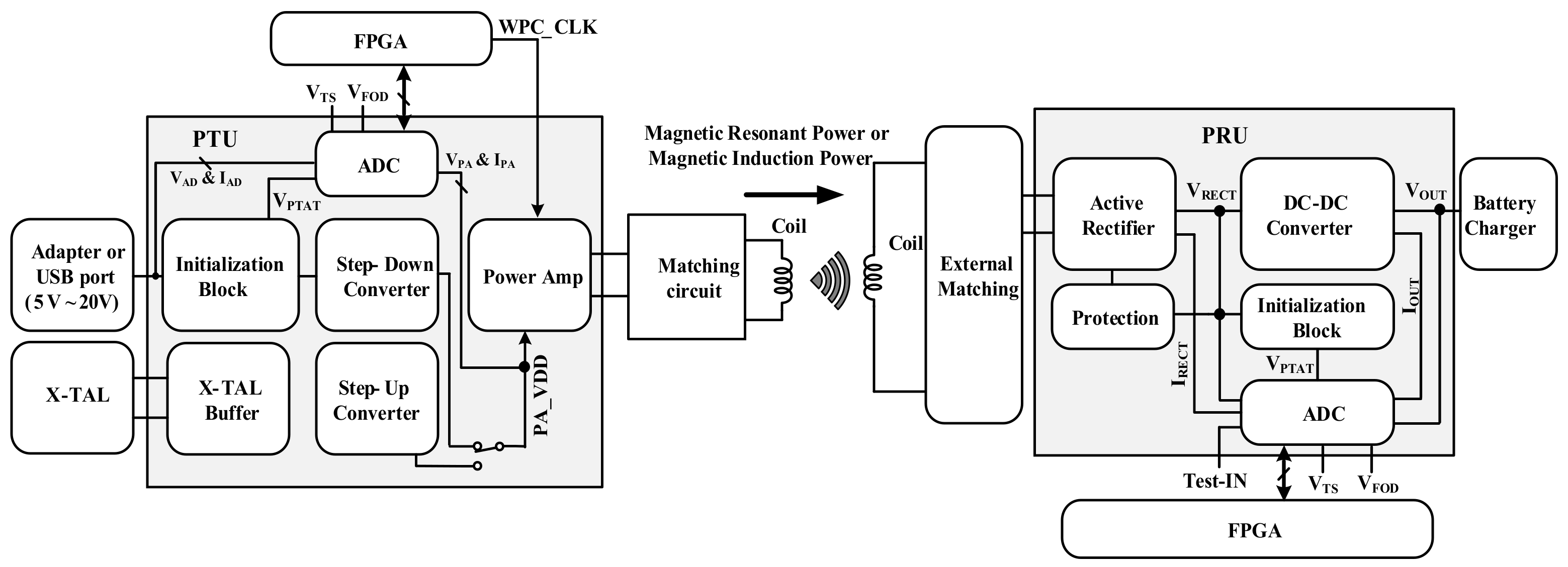
2.1. Block Diagram of the Wireless Power System
The simplified structure of a WPT system is presented in
Figure 1. This structure includes the power transmitter unit (PTU) and the power receiver unit (PRU). The PTU includes an initialization block, step-down and step-up converters, a power amplifier, and an ADC. The PRU includes an active rectifier, a DC–DC converter, an initialization block, protection and an ADC. Power is transferred through the power amplifier in the PTU and received through the rectifier in the PRU. The received power is rectified through a DC–DC converter, and is applied to charge a battery as shown in
Figure 1.
Different signals in the PTU and PRU need to be digitized through the ADC. For the PTU these signals are: adaptor voltage and current (VAD and IAD); proportional to absolute temperature voltage (VPTAT); voltage and current of the power amplifier (VPA and IPA); foreign object detection signal (VFOD); and, test signal (VTS). For the PRU they are: voltage and current of the rectifier (VRECT and IRECT); voltage and current of the DC–DC converter (VOUT and IOUT); VPTAT; VTS; and, VFOD. The identical ADC can be applied in both the PTU and PRU as the data converter. For this purpose and to reduce the required area and the number of the devices in the design, a multi-channel SAR ADC with a resolution of 10 bits for each channel has been proposed. This ADC module can also operate as a single 12-bit ADC. In the WPT system, some of the signals (such as VFOD) have to be digitized more accurately to have higher resolution. Therefore, the designed ADC module has the capability of also operating as a single channel 12-bit ADC.
2.2. Top Block Diagram of the Proposed ADC including Pre–Amplifier and Comparator
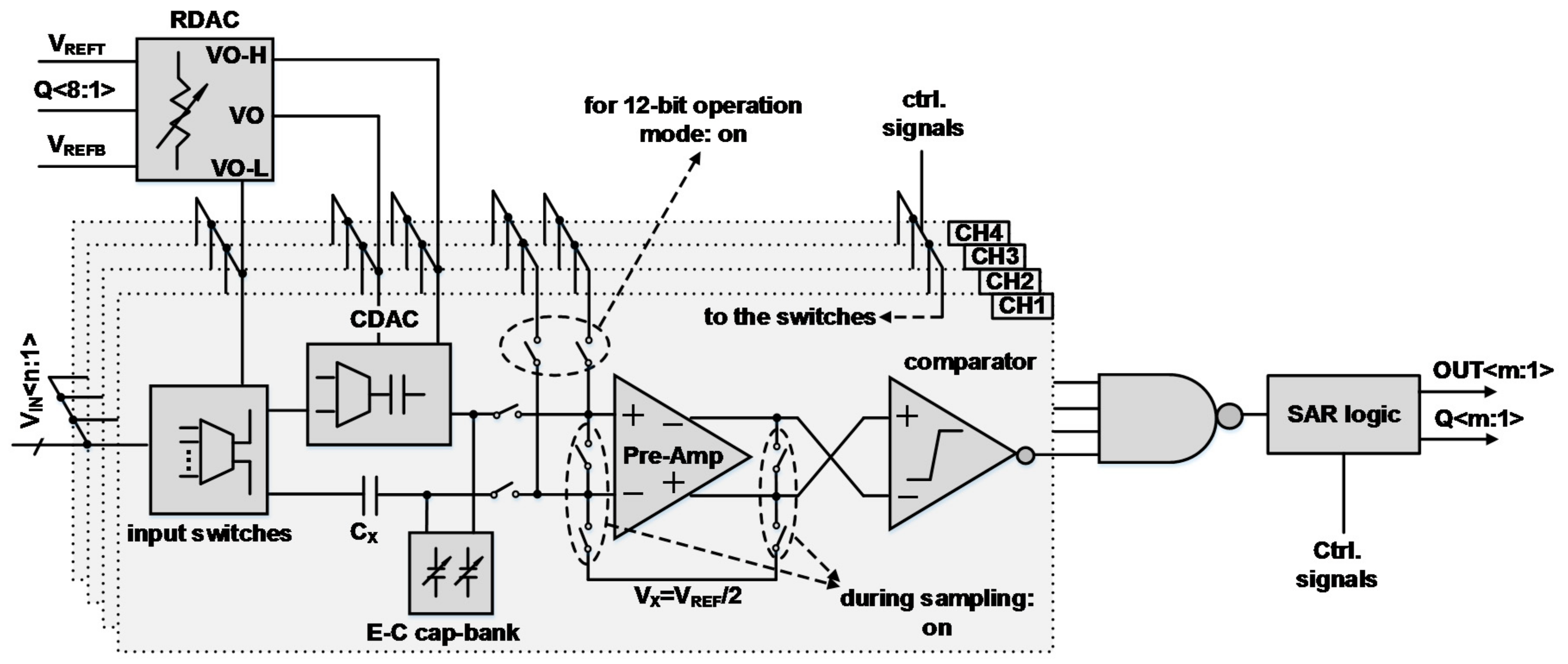
Figure 2 presents a simplified block diagram of the proposed multi-channel SAR ADC. This structure has four channels, and the resolution of each channel is 10-bit. Each channel has input switches, a CDAC, an error correction capacitor bank (E–C cap–bank), a pre–amplifier (Pre–Amp), and a comparator. The RDAC, reference generator, SAR logic, and digital parts are shared between all the channels. Three MSBs are determined in the CDAC, and multi–voltage levels are generated at the bottom plate of the dummy capacitor to produce the seven LSBs by using the RDAC. Simultaneous sampling of up to four analog input pins is possible for this ADC module using multiple sample and hold (S&H), where the inputs are sampled at the same time, and conversion is performed for each channel sequentially. Such data conversion can also be applied to multi-phase systems to sample the data for each phase at the same time.
As mentioned previously, this ADC can also operate as a single 12-bit ADC. In the WPT system, some of the signals (such as VFOD) have to be digitized more accurately to have higher resolution. Therefore, rather than designing a stand–alone 12-bit ADC, we have made the module flexible and combined the channels to also be able to apply it as a single 12-bit ADC. For the 12-bit configuration, CDACs of four channels are combined to make a single S&H with 32 unit capacitors, which are applied to determine the five MSBs. Like the 10-bit configuration, multi-voltage levels are generated at the bottom plate of the dummy capacitor to produce the seven LSBs by using the RDAC. Instead of designing a stand–alone 12-bit ADC, this approach reduces the required number of devices in the system and makes the design resolution flexible.
The supply voltage range for this design is 3–3.6 V. The conversion rate for 10-bit operation is up to 1 MS/s. Nevertheless, for reasonable performance, in 12-bit operation mode, the conversion speed has been designed to be half of that in the 10-bit mode. The operating temperature range of this structure is -40–85 °C. The clock frequency for 10-bit operation is 14 MHz. While two clock cycles are applied for sampling, 12 cycles are applied for charge redistribution and bit decisions. Therefore, the conversion rate of each channel is 1 MS/s. For 12-bit operation, 8.5 MHz clock frequency is applied. Three clock cycles are applied for sampling, and 14 cycles are applied for bit decisions. Therefore, the conversion rate of the 12-bit operation mode is 0.5 MS/s.
While sampling, and before charge redistribution starts, the top plates of the capacitors of the CDAC, as well as C
X, are connected to V
X, which is equal to half of the supply voltage (V
REF/2). The inputs are sampled at the bottom plate of the capacitors of the CDAC. After that, the top and bottom plates of the capacitors are disconnected from V
REF/2 and V
IN, and charge redistribution starts. C
X is charged to V
REF/2 and the CDAC output voltage is compared with this voltage for each bit decision. However, as this voltage is sampled at both the C
X and the top plates of CDAC, it is not required to be of exact value [
9].
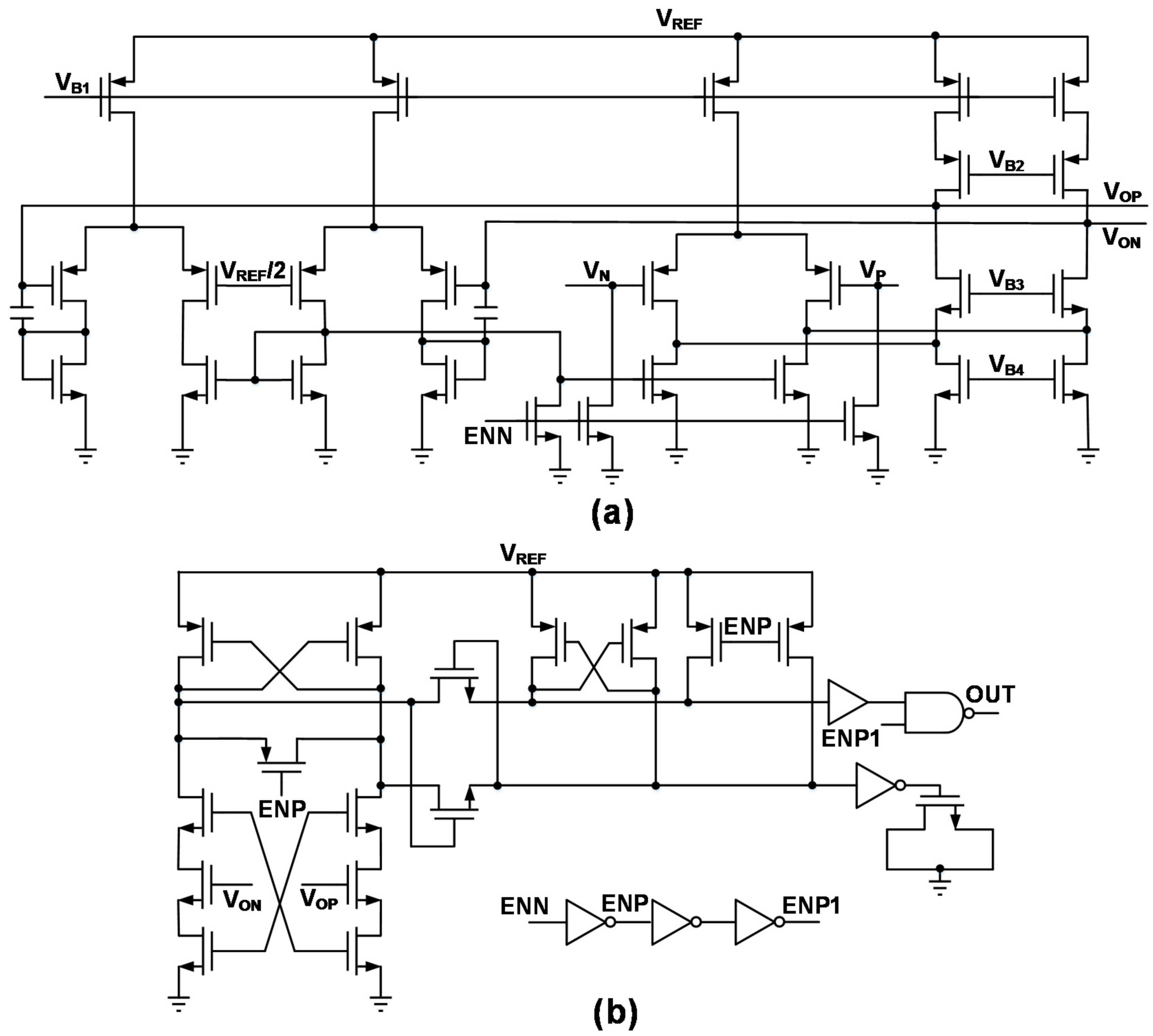
Figure 3a shows the structure of the pre-amplifier. This is a folded cascade structure with common-mode feedback. V
P and V
N are input signals, and V
B1, V
B2, V
B3, and V
B4 are bias voltages. ENN is the enable signal while V
OP and V
ON are the output pins.
Figure 3b presents the structure of the comparator, which includes the latches and the transistors necessary to control the enable and disable function. The outputs of the pre–amplifier (V
OP and V
ON) are connected to the input of this latch comparator. ENN is the enable signal, similar to that in the pre–amplifier. When ENN is zero, the comparator is active, and the comparison is performed. While the comparator is disabled, the comparator output (OUT) is equal to 1. The comparator of each channel has its own enable and disable signals and is controlled according to the operation algorithm of the ADC module.
2.3. Capacitor and Resistor DACs and Timing Diagram
This section explains the CDAC and the RDAC structures.
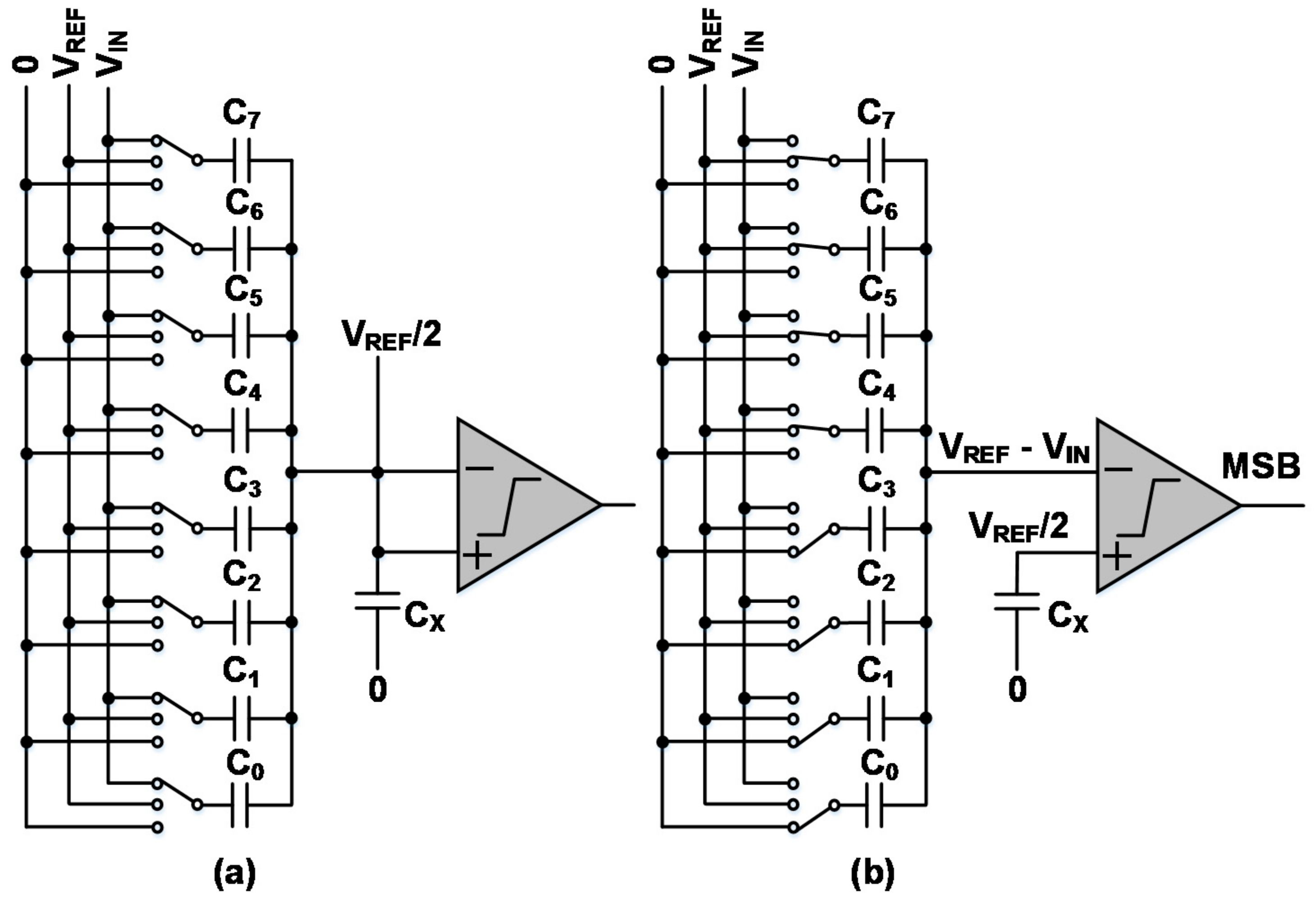
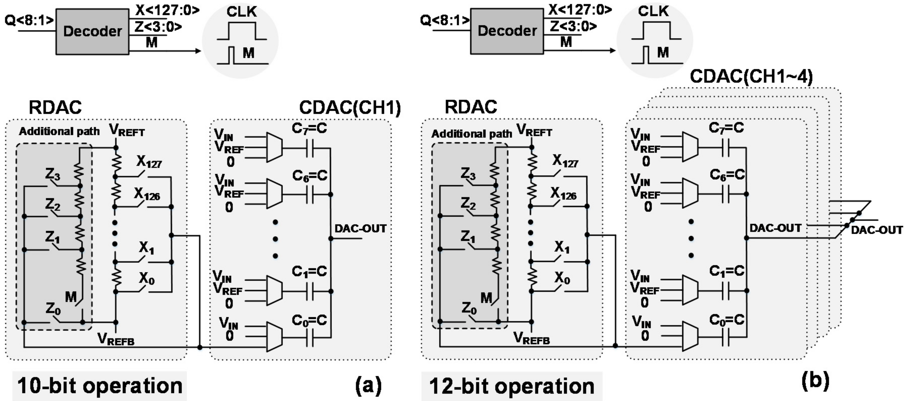
Figure 4a presents the structures of the CDAC and the RDAC, and their combinations for 10-bit operating mode in channel 1 (CH1). There are eight unit capacitors in the CDAC, where C
7–C
1 are applied to determine three MSBs. The remaining seven LSBs are determined through the RDAC and the dummy capacitor, C
0. Multi-voltage levels are generated according to the successive approximation algorithm using the RDAC, and change the voltage of the bottom plate of the dummy capacitor. Excluding the resistors in the additional path, there are 128 resistors in the RDAC. In each step, the reference voltage is decided in this block according to the previous decisions, and the voltage of the C
0 is changed.
In a binary-weighted DAC, no decoding logic is necessary. This is a major advantage of this structure that makes the binary-weighted DAC a simple structure. Nevertheless, there are still several major drawbacks to this structure. These drawbacks are all related to the major bit transitions. At the mid-code transition, the most significant capacitor value needs to be matched to the sum of all the other capacitor values within 0.5 LSBs. Because of the statistical spread, achieving such matching is difficult and cannot be guaranteed. Therefore, monotonicity is not guaranteed, which can result in a typical differential nonlinearity (DNL) plot. In addition, errors caused by the dynamic behavior of the switches result in glitches in the output signal. Such glitches contain highly nonlinear signal components, even for small output signals, and will manifest themselves as spurs in the frequency domain [
9,
10,
11].
In the proposed hybrid-type DAC, to avoid the mismatch and the abovementioned problems, the number of capacitors is selected to be only eight, and each unit capacitor size is 200 fF. To correct possible errors (due to settling) in the RDAC, an additional low resistive path is also applied. This path can support higher current and is enabled only for OUT < 7:6 > decision (through Q < 7 > and Q < 6 > switches). For the cases that OUT < 7:6 > predicts (11, 10, 01, and 00), Z
3, Z
2, Z
1, and Z
0 switches are turned on, respectively (together with the M switch).
Figure 4 shows that the M switch connects for a much shorter time than the clock period. It is notable that prior to each bit decision, these switches turn off, and only the main path is active at the time of decision. Therefore, the mismatch between this path and the main path is not of concern. Additionally, for the same reason, the reference voltages of this path do not need to be exact values.
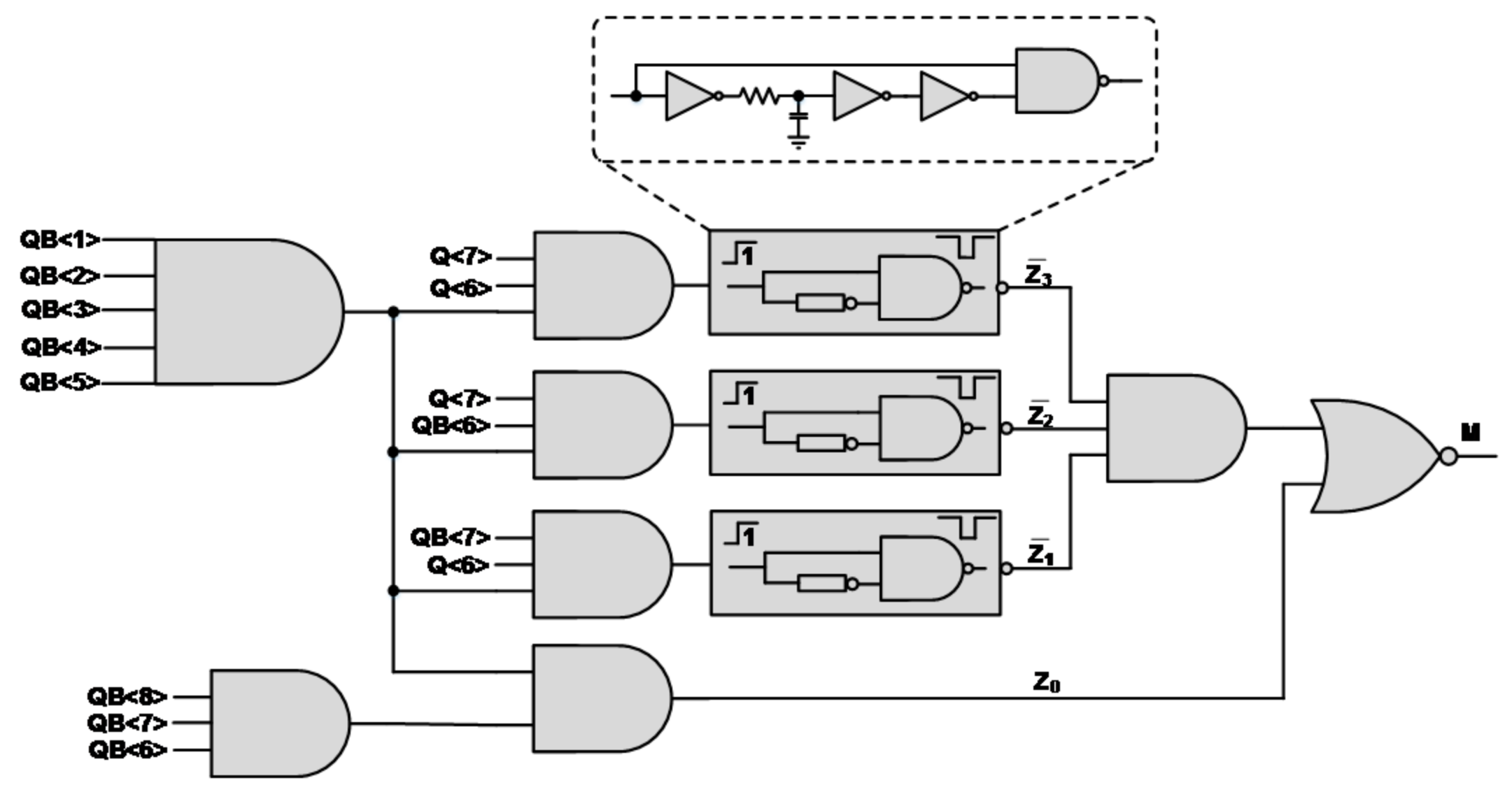
Figure 5 shows the algorithm controlling the Z < 3:0 > and M switches.
As can be seen, the total number of unit capacitors in four CDACs is 32, and the total number of resistors in the RDAC is 128. However, if the RDAC had not been shared, there would have been 512 resistors in this structure. In addition, if we had applied only CDACs instead of the hybrid structure, for each CDAC and for the total channels, 1024 and 4096 unit capacitors would have been required respectively. In this case, the mismatch between MSB and LSB capacitors would have been critical. Therefore, this structure reduces the number of the required devices in the system. It is notable that increasing the conversion rate while applying only one ADC to the system cannot satisfy the requirements of the system.
Figure 4b presents the structures of the CDACs and the RDAC, and their combinations for the 12-bit operating mode. The CDACs of the channels (1–4) are combined and shared. Therefore, in this case, there are 32 unit capacitors in the CDAC. These 32 unit capacitors are applied to decide five MSBs, while the RDAC, together with the dummy capacitor, decides the seven LSBs in a manner similar to that of the 10-bit operation.
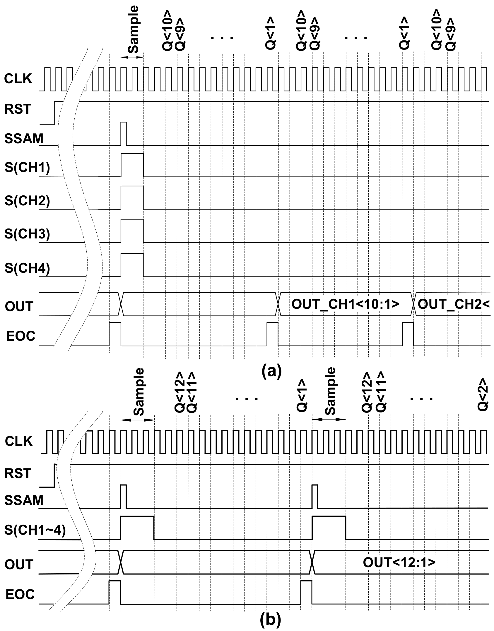
Figure 6 presents the timing diagram of the designed ADC.
Figure 6a shows that four inputs are sampled simultaneously, and the output bit decisions are performed in order from CH
1 to CH
4. Sampling is done within two clock cycles, and charge redistribution is done in 12 clock cycles. This is an example of 10-bit operating mode timing, for the case where simultaneous sampling is required. However, the structure has a flexible operation, according to the sampling and digitization requirements.
Figure 6b summarizes the timing diagram of the 12-bit operation mode. The input is sampled in the CDACs of the channels (1–4) within three clock cycles. Then, the charge redistribution is done within 14 clock cycles. The clock frequencies for the 10-bit and 12-bit operating modes are 14 and 8.5 MHz, respectively. The conversion rates of the 10-bit and 12-bit operating modes are 1 MS/s and 500 kS/s, respectively. It is notable that the possible timing mismatch between the channels does not affect performance because the LSBs are decided in a single RDAC shared between all the channels.
2.4. Switching Sequence in CDAC and RDAC
Figure 7 presents the simplified sampling and holding process of one of the channels. During the sampling phase, the bottom plates of all the capacitors are connected to the input voltage, and the top plates are connected to V
REF/2. In addition, V
REF/2 is also sampled in the C
X capacitor. During the holding phase, the top plates of all capacitors, including C
X, are disconnected from V
REF/2, and the bottom plates of half of the capacitors are switched to V
REF, and the other half are switched to 0. At the end of this phase, V
IN is compared with V
REF/2 and MSB is decided. It is notable that for simplicity, the pre–amplifier, inverting comparator, and other switches are simply replaced by a comparator.
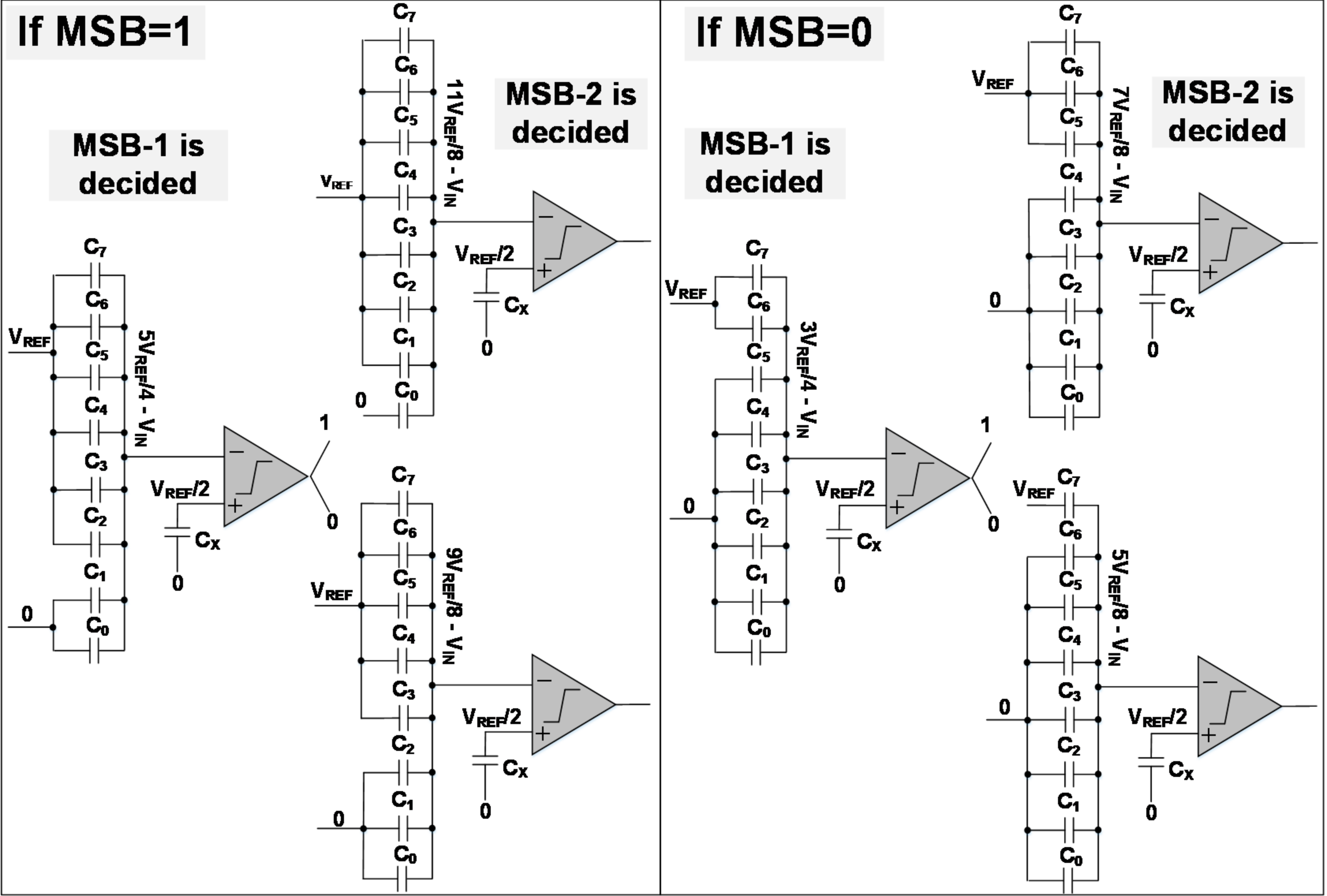
Figure 8 summarizes the rest of the switching for the three MSB’s determination. For example, for the case in which three MSBs are 111, the bottom plates of 7/8 capacitors are switched to V
REF. The rest of the bit decisions are done in the RDAC, together with C
0. The multi–voltage levels are decided in the RDAC according to the successive approximation algorithm and the voltage of the C
0 is changed. It is notable that, if the MSB-2 bit is determined to be zero, then the bottom plate of one of the capacitors in
Figure 8 that is connected to V
REF is switched back to zero, and then bit decision is continued in the RDAC.
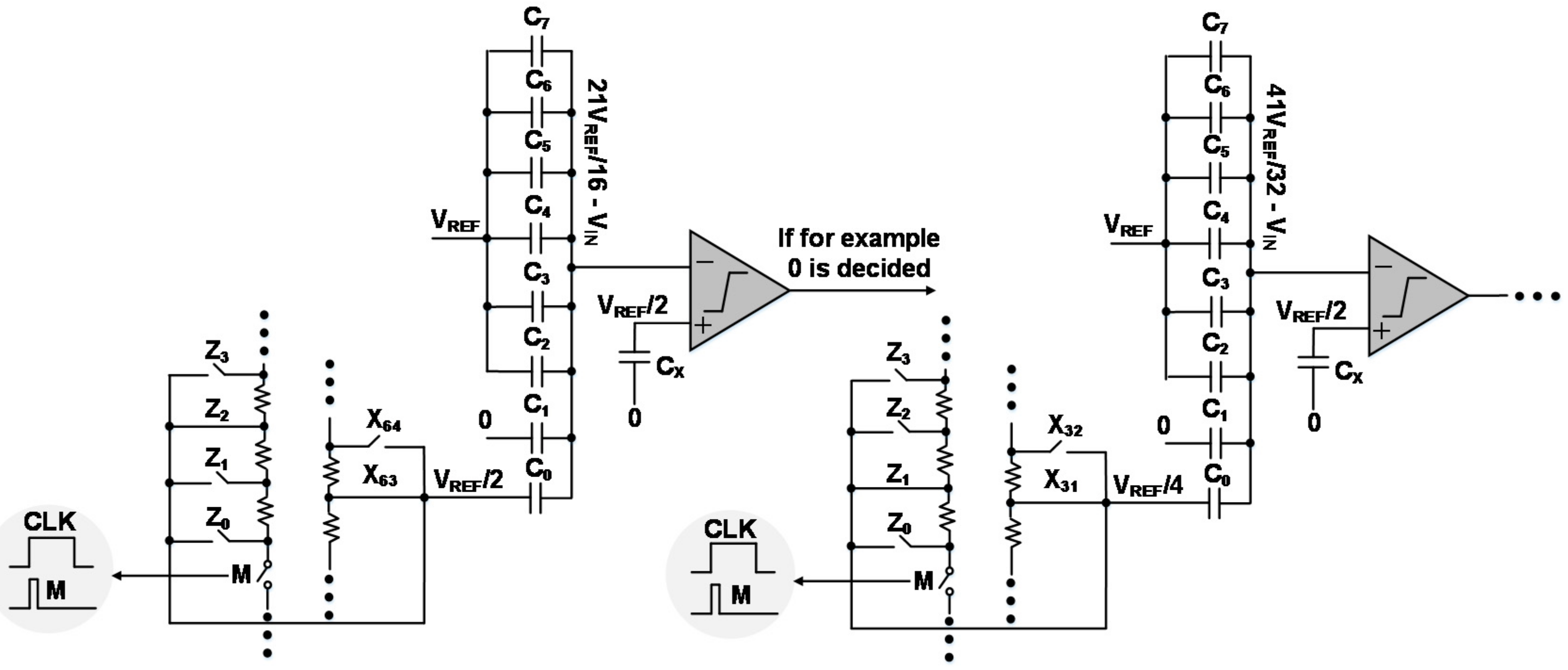
Figure 9 shows an example of bit decision in the RDAC. For this case, we assume that the three MSBs are 110. As MSB-2 is zero, the bottom plate of C
1 switches back to zero. The RDAC provides V
REF/2, and feeds it to C
0, where X
63 switches on. Now 21 × V
REF/16 − V
IN is compared with V
REF/2 in the terminals of the comparator. This means that V
IN is compared with 13 × V
REF/16. During this cycle, the Z
2 and M switches of
Figure 4 also switch on for a short period to provide an extra low resistive path, increase the settling time, and reduce the possible errors.
Assume that, in this case, the comparator output is decided to be zero. This means that four MSBs have been determined to be 1100. Then, the RDAC is switched back to half of the VREF/2 (VREF/4), where X63 switches off, and X31 switches on. This voltage is fed to C0. Now, 41 × VREF/32 − VIN is compared with VREF/2 in the terminals of the comparator. This means that VIN is compared with 25 × VREF/32, and the next bit is decided. Here, as well, Z1 and M switch on for a short period to provide an extra low resistive path, increase the settling time, and reduce the possible errors. The process of the seven LSB’s determination in the RDAC operates in a similar way, according to the successive approximation algorithm.
As mentioned before, multi–voltage levels are generated at the bottom plate of the dummy capacitor to produce the LSBs by using the RDAC, which reduces the number of the capacitors. The control logic in the RDAC is also according to the successive approximation algorithm. Although this logic applies more devices in the RDAC compared to the CDAC, the overall area of the ADC module is reduced, as this block is shared between all the channels.
Although more power efficient switching for the CDAC has been presented in recent work [
12,
13,
14], because of the low switching frequency of this structure and the low number of the capacitors in the CDAC, the power consumption of this part is not the major power consuming part of the circuit. (This is shown in the following section.) Therefore, to avoid the complexity of the power efficient switching structures, the abovementioned switching is applied in this structure.
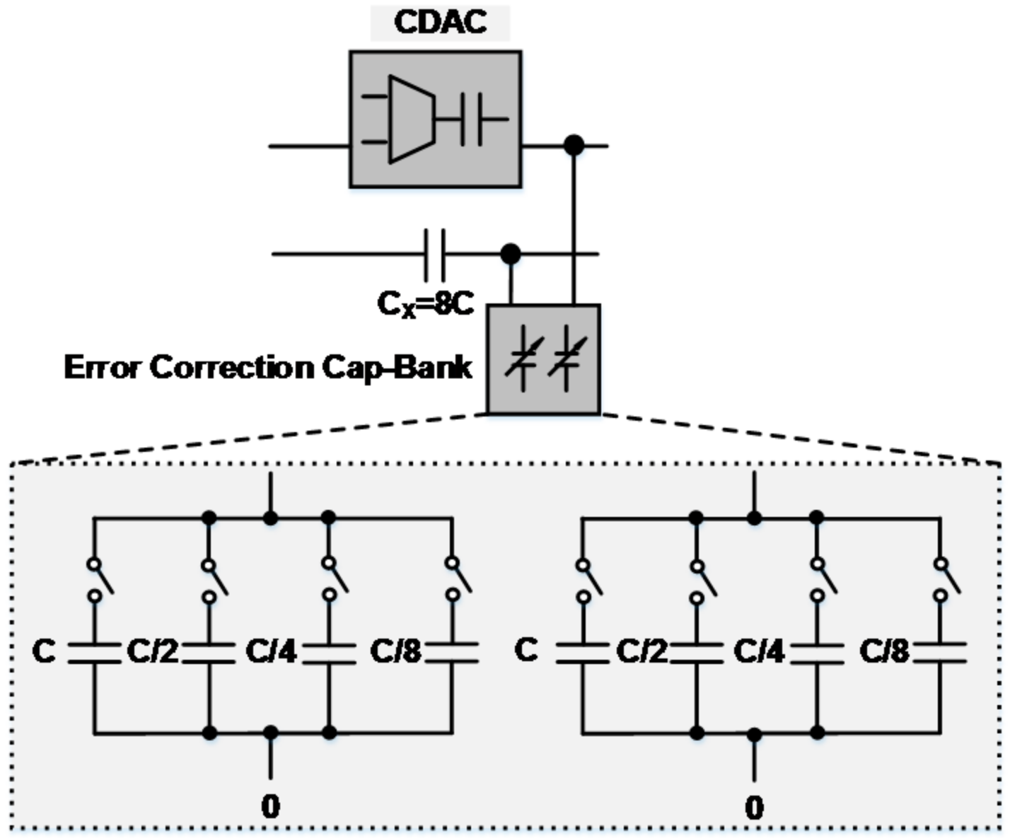
2.5. Error Correction Capacitor Bank, Mismatch and Noise Consideration
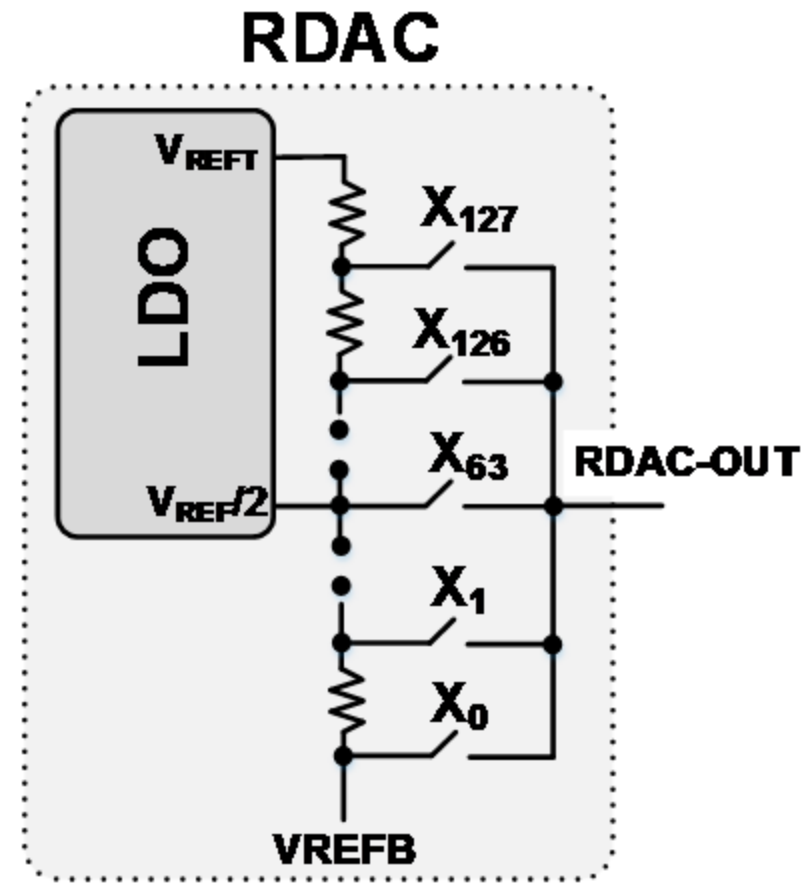
Figure 10 presents the attenuation and the error correction capacitor bank structure. To be able to control the structure following fabrication and in measurement levels, some trimming has been applied to the structure. The capacitors in these capacitor banks can be applied to reduce the gain and the offset errors of the ADC up to 1/8 unit capacitor sizes. This is applied as the coarse offset cancelation. The fine offset cancelation is done in the RDAC, through the control of V
REFT and V
REFB.
Furthermore, there is the possibility that the input signal to the ADC is not a full range sine wave. For this case, the input range of the ADC can be reduced to match the input signal level, to use the maximum dynamic range of the output digital codes. Even though this would reduce the LSB voltage value (Vp − p/1024), the system is tolerant of this reduction, because the ADC module is designed to have 12-bit linearity. These capacitor banks can also be applied to attenuate the charging and discharging voltage values in the CDAC and CX, to avoid certain possible errors. In the ADC measurement level, the switches of these capacitor banks are controlled manually with a serial peripheral interface (SPI) and provide the foreground calibration for the CDACs.
Considering the mismatch in the capacitor bank, in the extreme case for 10-bit operation mode, four unit capacitors to determine MSBs can have a 4 × (C ± ∆C) value, while the unit capacitor to decide MSB-2 can have a C ± ∆C value. For this case, as an example, the voltage ratio can be 4 × V
REF × [(C − ∆C) / (C + ∆C)]. Therefore, the [4C/C] × V
REF − 4×V
REF × [(C − ∆C) / (C + ∆C)] should be less than +0.5 LSB, which for 3 V reference voltage, and the 10-bit operation mode, is 0.5 × 3/1024 ≃ 1.5 mV. However, based on the theory in Ref. [
9], and from the behavioral–model simulations in Ref. [
15], it is verified that in a 12-bit ADC, 1% matching is sufficient to keep the integral nonlinearity (INL) and differential nonlinearity (DNL) within 1 LSB. Therefore, 200 fF has been applied as the unit capacitor to ensure the process variation would not affect the ADC performance.
The total capacitance of the CDAC, together with routing, is designed to be nearly 1.6 pF. With this capacitor size, and according to the Refs. [
3] and [
16], the noise power due to the sampling [kT/C] in the CDAC is almost P
ns = 2.58 × 10
−9 [V
2]. In addition, considering the full-scale sinusoid, the maximum input signal power is 1.62 [V
2]. Since the noise is 88 dB below the signal level, this ensures more than 12-bit resolution for the ADC, and kT/C is not a limiting factor in this structure. On the other hand, the voltages of the RDAC are controlled by a constant voltage from a low drop-out (LDO) voltage regulator, as shown in
Figure 11. The flicker noise can be further reduced by applying choppers in the pre–amplifier. However, for the required resolution in a WPT system, the noise level is satisfactory.
3. Simulation Result
This ADC is designed and tested with a 180 nm CMOS process.
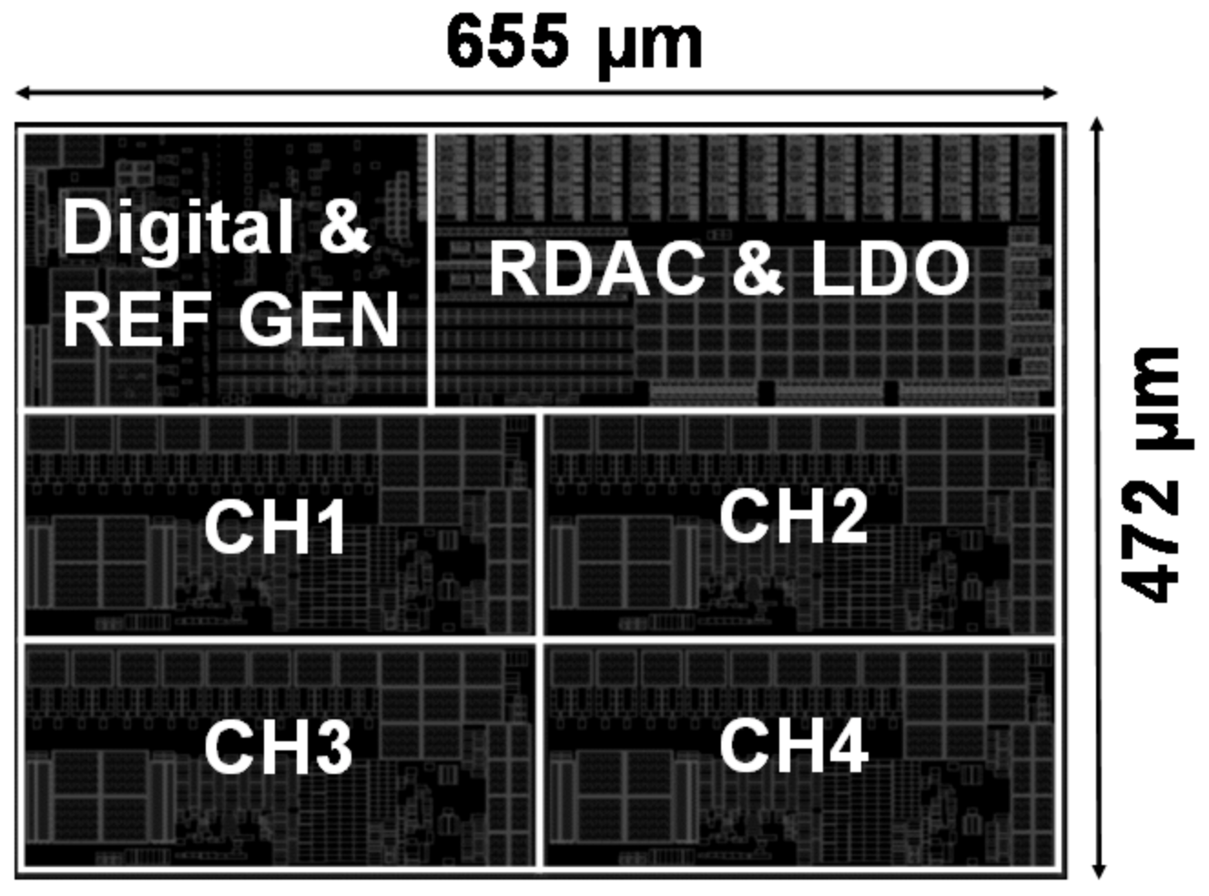
Figure 12 presents the layout of this ADC. The size of this four-channel ADC, including the RDAC, the digital control part, and the reference generator (REF GEN), is only 655 µm × 472 µm, which is a very small value.
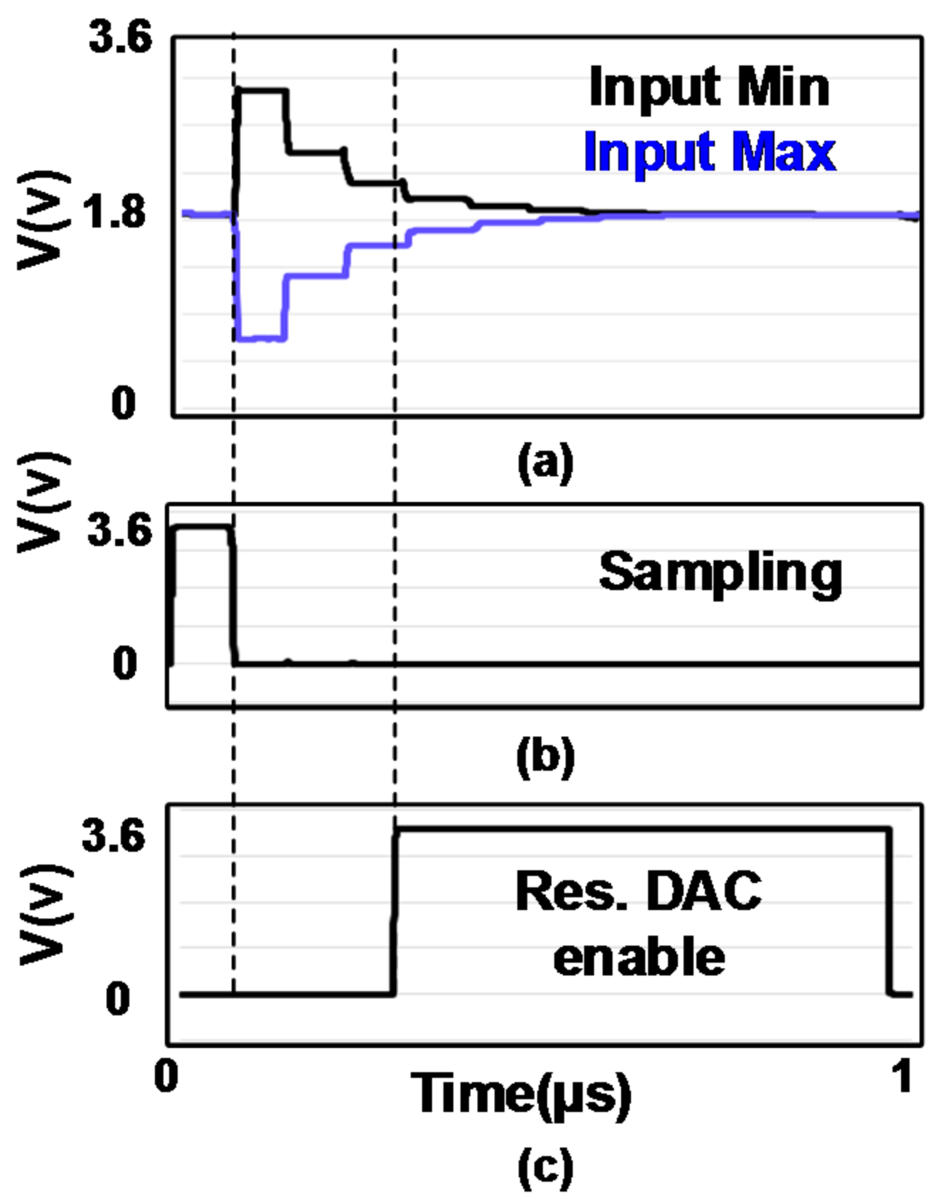
Figure 13a shows the CDAC output settling for the maximum and minimum values of the input signal.
Figure 13b,c also present the sampling and the RDAC enable signals.
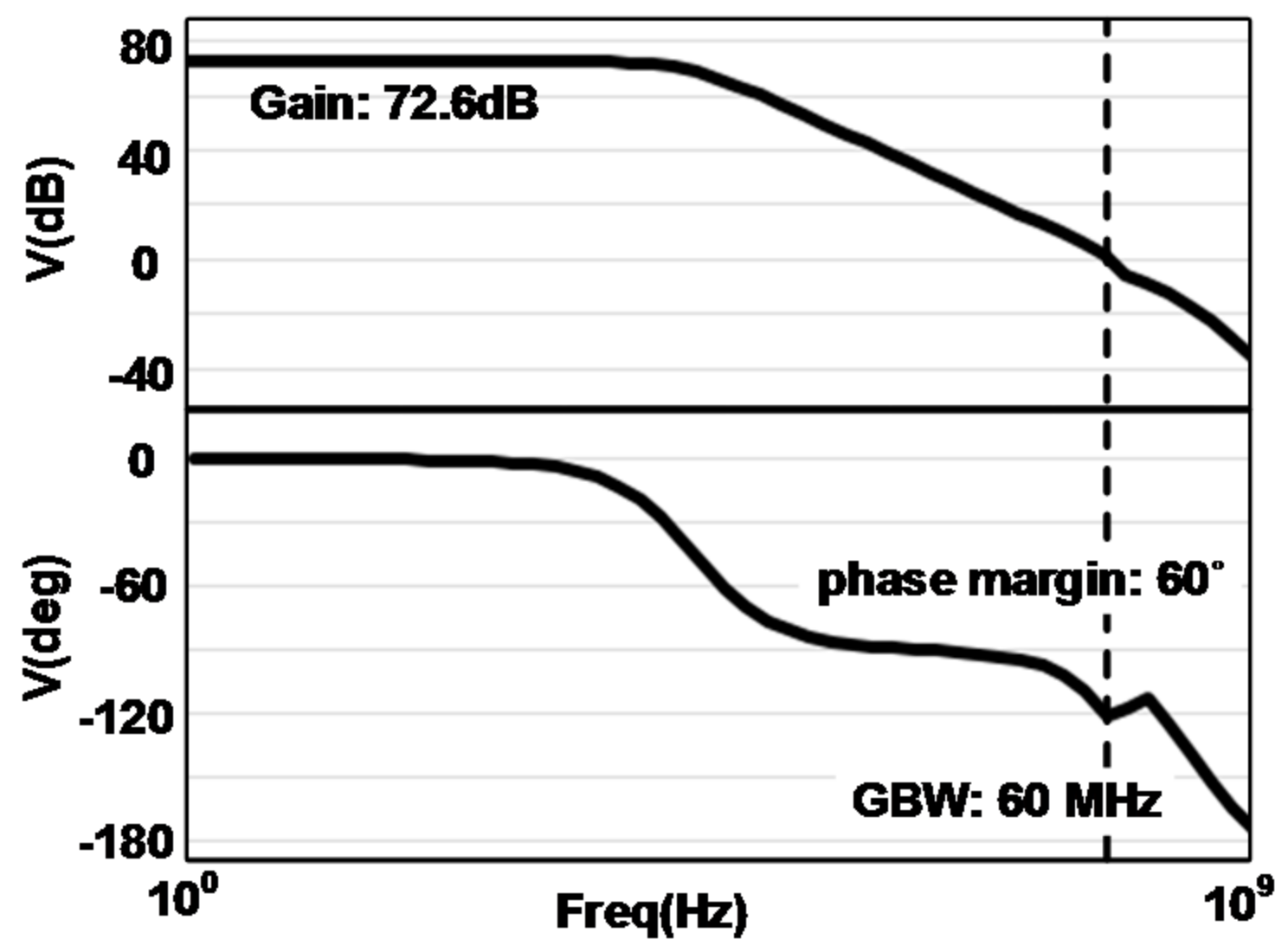
Figure 14 shows the gain and the phase margin of the pre-amplifiers. In this amplifier, for the common-mode loop, the gain is 72.6 dB and the phase margin is 60°. Even though, due to the latches in the comparator, the lower gain could also be applied in the pre–amplifier, it has been designed for the worst cases where one LSB is around (or even below) 0.7 mV, and some margin has been also considered. The gain bandwidth of this amplifier is 60 MHz.
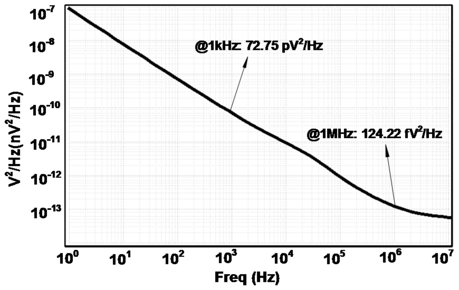
Figure 15 shows the noise simulation of the analog parts for channel 1. This shows that the noise for the whole range is in the nV
2/Hz range, and for special frequencies, such as 1 kHz and 1 MHz, these values are 72 pV
2/Hz and 124 fV
2/Hz, respectively.
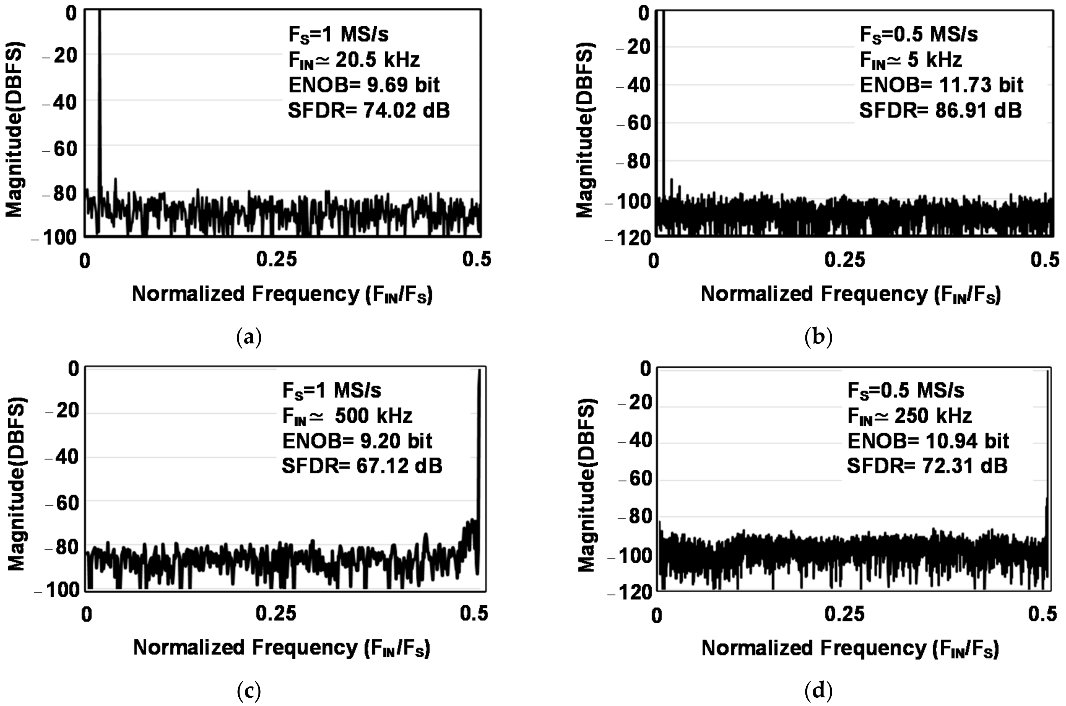
Figure 16a shows the fast Fourier transform (FFT) spectrum with 1024 samples, and for the 10-bit operation mode. The sampling frequency for this simulation is 1 MS/s and the input frequency is 20.5 kHz. The effective number of bits (ENOBs), signal to noise and distortion ratio (SNDR), and spurious free dynamic range (SFDR) for this simulation are 9.69 bits, 60.10 dB, and 74.02 dB, respectively.
Figure 16b shows the FFT spectrum with 4096 samples, and for the 12-bit operation mode. The sampling frequency for this simulation is 0.5 MS/s and the input frequency is 5 kHz. The ENOB, SNDR, and SFDR for this simulation are 11.73 bits, 72.38 dB, and 86.91 dB, respectively. Furthermore,
Figure 16c,d shows the Nyquist input frequency simulations for 10- and 12-bit resolutions, respectively. The ENOB for these cases are 9.20 and 10.94 bits, respectively. Nevertheless, the requirements of the ADC for the WPT application applies in lower frequencies, and ADC will not operate in Nyquist frequencies. It is notable that the analog parts, parasitic R and CC, are extracted through Cadence Calibre and are considered in all the simulations.
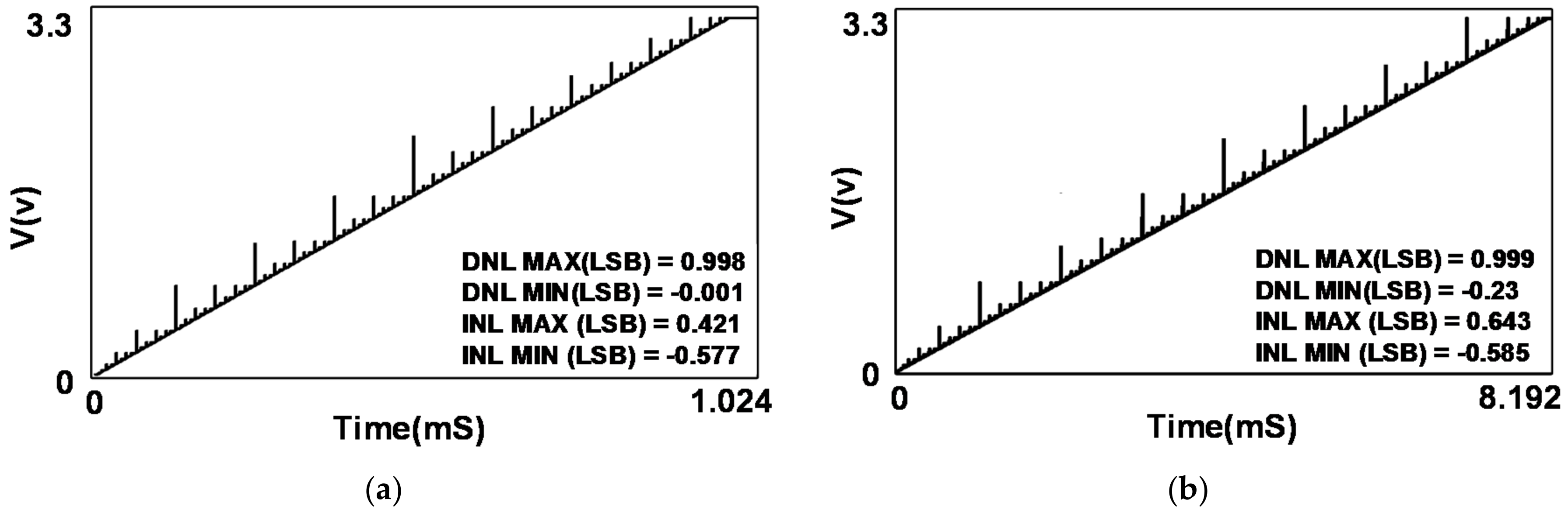
Figure 17 presents the ramp simulations for both 10-bit and 12-bit operation modes to determine linearity.
Figure 17a shows the ramp simulation for 10-bit operation mode. The conversion rate for this simulation is 1 MS/s and the number of samples is 1024. As is summarized in
Figure 17a, the DNL and INL are in the ranges of −0.001–0.998 and −0.577–0.421, respectively.
Figure 17b presents the ramp simulation for 12-bit operation mode. The conversion rate for this simulation is 0.5 MS/s and the number of samples is 4096. As is summarized in
Figure 17b, the DNL and INL are in the ranges of −0.23–0.999 and −0.585–0.643, respectively. However, by increasing the current of the RDAC, the overall performance improves. It is notable that also for these simulations, the analog parts, parasitic R and CC, are extracted through Cadence Calibre and are considered in the simulations.
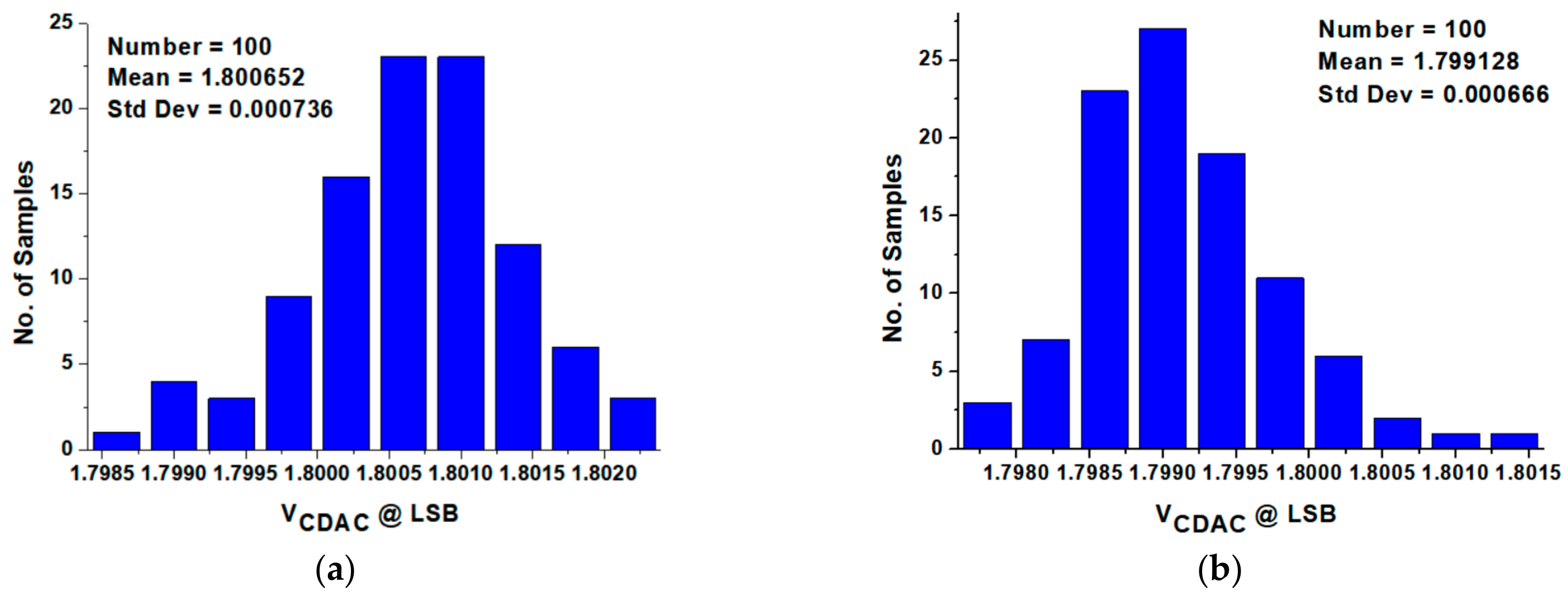
Figure 18a,b illustrates the mismatch, and process variation results which are implemented by Monte Carlo simulations. For these simulations, two cases are considered and the output voltage of the CDAC for LSB decision is presented. The LSB comparison and bit decision is done around V
CM.
Figure 18a is for the case where all the output bits should be high. In this simulation, the number of samples is 100, the mean value is 1.800652 and the standard deviation (Std Dev) is 736 µV, which is less than one LSB for the 12-bit operating mode.
Figure 18b is for the case where all the output bits should be low. In this simulation, the number of samples is 100, the mean value is 1.799128 and the standard deviation is 666 µV, which is less than one LSB for the 12-bit operating mode.
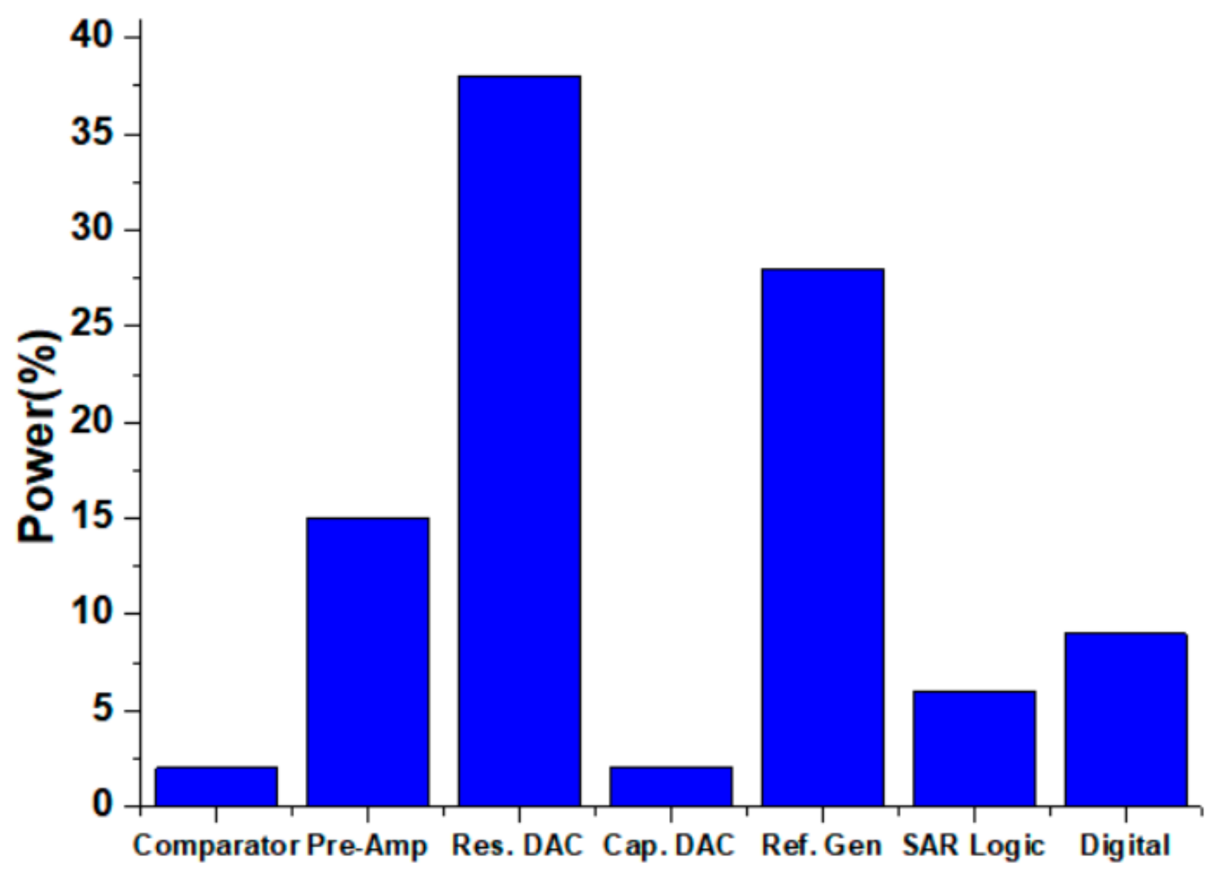
Figure 19 presents the power break-down of the design for 10-bit operating mode. As can be seen, RDAC, reference generator, and pre–amplifier power consumptions are dominant. The power consumption of one channel of the system for the 10-bit operation mode and with 1 MS/s conversion speed is 262 µW. The core ADC power consumption for this case is 189 µW. The power consumption of the system for the 12-bit operation mode and with 0.5 MS/s conversion speed is 404 µW. The core ADC power consumption for this case is 291 µW. To calculate the figure of merit (FOM) of the core ADC, the power consumption implemented in
Table 1 excludes the power consumption of the reference generators. To improve the linearity and the performance of the ADC, the current consumption of the RDAC, as well as the overall system, can be increased.
Finally,
Table 1 summarizes the performance of the structure for both 10- and 12-bit operation modes and compares them with some of the structures with similar performances. The area of the ADC module is the most interesting specification of this work and has been presented in
Table 1. The contribution of this work is to reduce the area of the multi-channel ADC for a WPT system and this design shows a remarkable low-area performance. As shown, the area of the four-channel ADC is only 0.31 mm
2, which is very small compared to other ADCs that are only single-channel ADC structures. This has been achieved by applying shared RDACs and shared CDACs in a hybrid-type multi-channel, multi-resolution ADC module. The other specifications of the designed ADC module, such as ENOB and FOM, are also comparable with other structures. However, instead of applying a pre–amplifier and latches, the application of a fully dynamic comparator would reduce power consumption further and improve the FOM for this design, which is the intention of future research work. It is notable that, for a fair comparison, the references in
Table 1 have been selected from studies that have similar resolutions and conversion rates, as there are a variety of ADCs with different resolutions and conversion rates.


 ,
, 


