Article

Control of the Bidirectional Buck-Boost Converter Operating in Boundary Conduction Mode to Provide Hold-Up Time Extension

by
Oswaldo Lopez-Santos
1,*,
José Omar Urrego-Aponte
2,
Sebastián Tilaguy-Lezama
1 and
José David Almansa-López
1
1
Facultad de Ingeniería, Universidad de Ibagué, Carrera 22 Calle 69 Barrio Ambalá, Ibagué 730001, Colombia
2
SERMA Ingénierie, 3 Impasse Marcel Chalard, 31110 Toulouse, France
*
Author to whom correspondence should be addressed.
Energies 2018, 11(10), 2560; https://doi.org/10.3390/en11102560
Submission received: 11 September 2018 / Revised: 20 September 2018 / Accepted: 21 September 2018 / Published: 26 September 2018

Abstract

:
A hold-up time extension circuit (HTEC) is used to charge and discharge an auxiliary capacitor. This capacitor stores the energy required to extend the operation time of critical loads experiencing short duration failures (SDF) at the DC bus to which they are connected. This paper presents complete modeling and a control-wise approach to a parallel HTEC based on the bidirectional buck-boost converter, which operates in Boundary Conduction Mode (BCM) with a variable switching frequency. The circuit permanently regulates the voltage of the auxiliary capacitor as well as the voltage of the DC bus during SDF, which is uncommon in industrial versions of HTEC. Enforcing the operation in BCM allows a reduction in the size of the inductor in the converter without requiring additional control circuitry. The entire behavior of the proposed HTEC, in all its operation modes, was analyzed theoretically and validated using simulation and experimental results, showing the potential of the circuit to be used in real applications.

1. Introduction

The occurrence of temporary interruptions and other short duration failures (SDF) in the input source of critical DC loads affects the reliability of many electrical systems considerably. This is the case for regulated DC sources fed by non-regulated buses, which are installed onboard commercial and civil aircraft to feed measurement instruments. Hence, current regulations require that this equipment support the SFD [1,2] to some extent. Since DC power systems are increasingly implemented in terrestrial vehicles and in commercial and residential buildings, solutions that provide robustness to SDF have become relevant [3,4]. Although the majority of DC-sourced devices have included an input capacitance of considerable value, providing a short hold-up time after failure [5], manufacturers now focus on reducing the size and weight of devices, even at expense of hold-up features. Special techniques and methods have been developed to overcome this issue [6]. However, when the continuous operation of a load is critical, the hold-up time has been extended by means of external additional devices—so-called hold-up time extension circuits (HTEC) [7,8,9].
Most of the existing HTEC use an auxiliary capacitor for energy storage. This element is charged during normal operation of the DC bus and discharged during SFD. Depending on the topology connecting the bus, the HTEC, and the load, solutions can be classified as either series-architecture or parallel-architecture. The limitation of series-architectures is the size of the capacitor due to the limited voltage level of the DC bus. In addition, there is an obvious loss of efficiency because all the power consumed by the load passes through the HTEC. However, because of the direct connection of the circuit with the input of the critical load, reliability is higher when compared with other architectures [10]. Parallel off-line architectures charge the capacitor using the HTEC, keeping it in standby until an SDF occurs. Then, the load is connected to the capacitor through a switch, which produces an undesired transitory behavior. This is the most common architecture of commercial HTEC [11,12]. The parallel on-line architectures of HTEC have a converter to charge and discharge the auxiliary capacitor to a higher voltage level, allowing more energy to be stored with the same capacitance [13]. Then, the required converter in these architectures must have boost capabilities and bidirectional power flow. Among the existing possibilities, some special topologies, such as the converter presented in Reference [14], may provide a high-gain at the expense of additional complexity. Due to the main property of the non-inverting synchronous buck-boost converter, which ensures the same electrical reference for the source and the load, this can be one of the preferred topologies [15]. However, because of the intended intermittent operation, criteria such as simplicity and a reduced number of components become more relevant, as in Reference [16], where the authors employed a conventional synchronous boost converter. In this case, as in some applications for microgrids, the symmetry of the circuit configuration for the charging and discharging mode of the conventional bidirectional buck-boost converter (BBBC) is a relevant criterion since it leads to simpler control [17].
A first version of the proposed control operating on a BBBC in boundary conduction mode (BCM) was presented in Reference [18]. Only three operational modes, with some transitions defined between them, were identified, namely a charging mode, a standby mode, and a discharging mode. However, the power converter and the auxiliary capacitor were considered as ideal elements, making it difficult to understand the need for the additional operational modes. After a deeper analysis, including experimental testing, an improved version of the control was developed considering the power conduction losses in the inductor and the auto-discharge parasitic resistance of the capacitor. As a result, a new operational mode has been included in the decision-event approach and a linear voltage regulator has been replaced by a hysteresis controller, considerably improving the overall performance of the HTEC. The rest of the paper is organized as follows: Section 2 presents a description of the operational modes of the HTEC; modeling and control of the HTEC are described in detail in Section 3. Section 4 focuses on simulation and experimental results, validating the theoretical analysis. Finally, conclusions and future work are presented in Section 5.

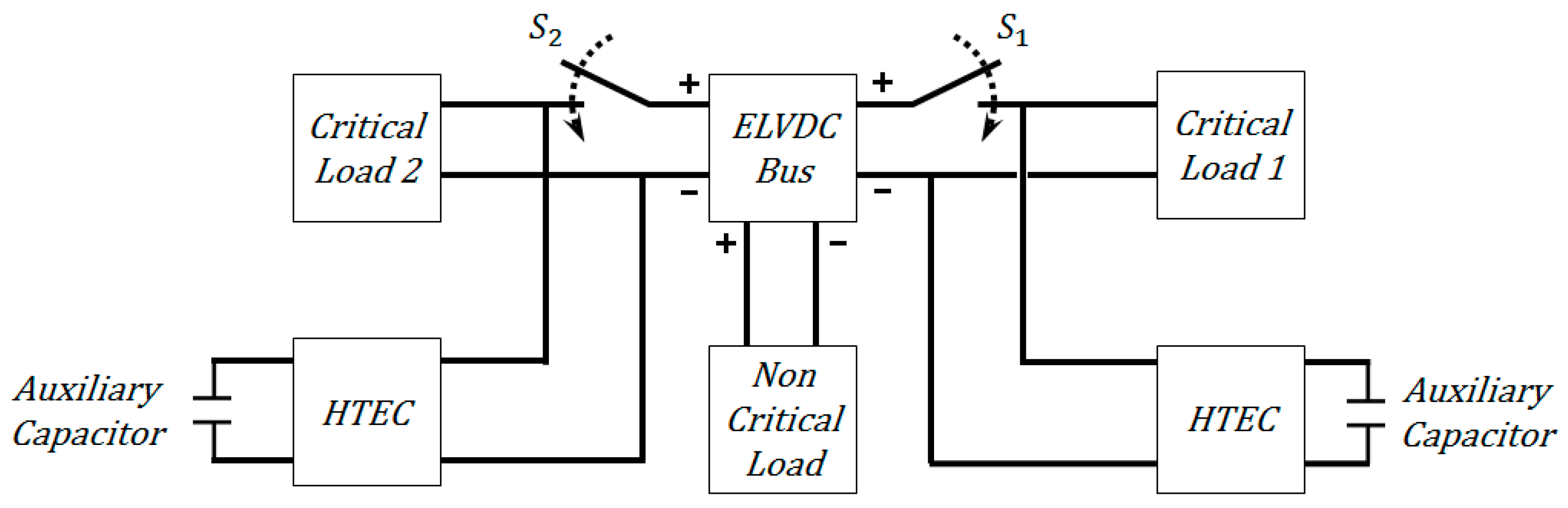
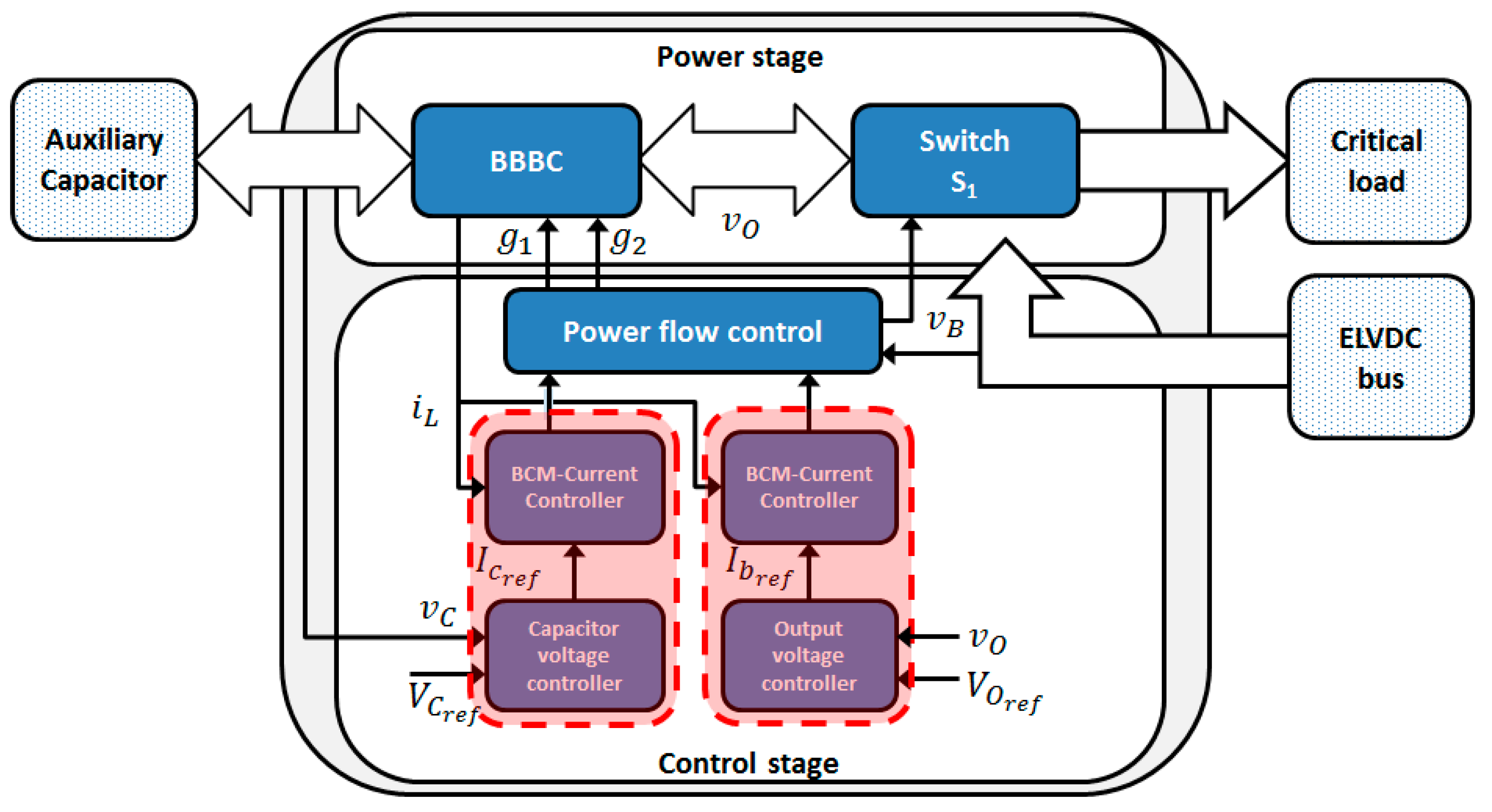
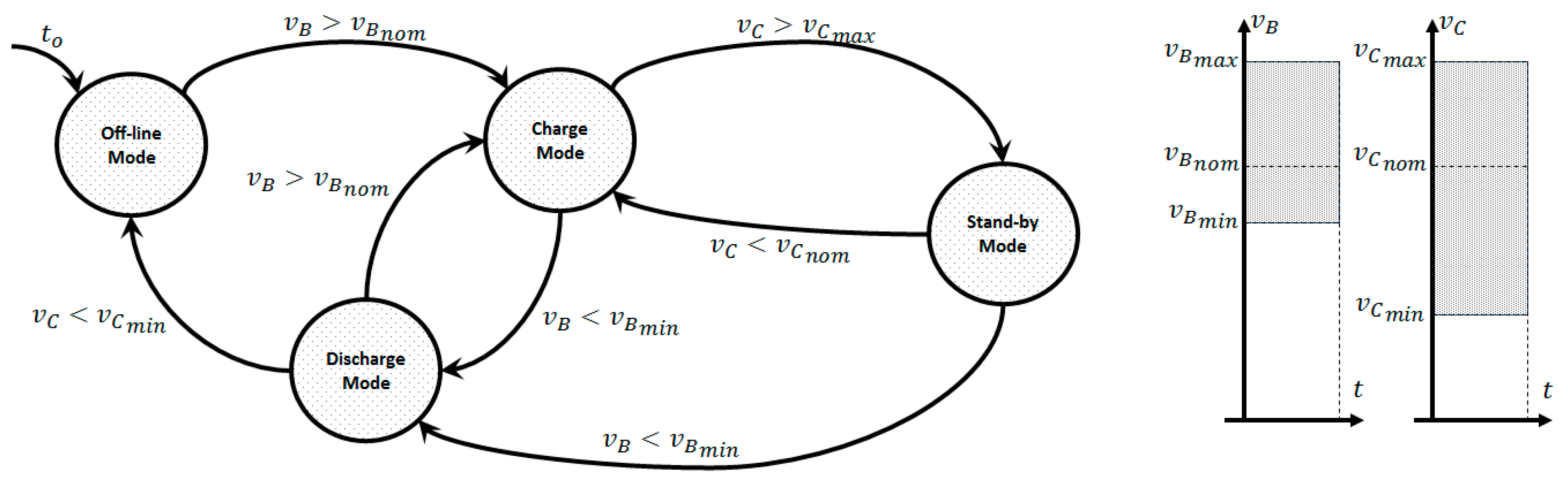
2. General Description of the Control System

Figure 1 shows a block diagram of an Extra Low Voltage DC (ELVDC) bus in which both critical and noncritical loads are connected. HTEC devices are connected in parallel to critical loads and have a dedicated auxiliary capacitor external to the circuit. In this context, when the ELVDC bus operates normally, its voltage is the same voltage as the load. However, when an undesired voltage level is detected, the switch S 1 has the function of differentiating the voltage of the critical load and the voltage of the bus. Then, due to the bidirectional power flow of HTEC devices, the input voltage of each load can be regulated during failure.
Figure 2 shows a detailed block diagram of an HTEC interconnection with the ELVDC bus and one critical load. The HTEC consists of a power stage and a control stage. The power stage consists of a DC-DC converter and the switch S 1 , which is bidirectional in terms of current and unidirectional in terms of voltage. The control module is composed of a block of power-flow control, which selects the controller to charge or discharge the capacitor. The control module provides the gate with signals for the power module; it also provides the gate signal for the switch.
The circuit model of the BBBC connected to an ELVDC bus is depicted in Figure 3. Notice that the diode of the conventional buck-boost has been replaced by the MOSFET (Metal Oxide Semiconductor Field Effect Transistor), M 2 , to allow a bidirectional power-flow capability. The capacitor, C a u x , is the storage element of the circuit, which has an auto-discharge resistance ( R c p ). The capacitance, C b u s , represents the bus capacitance, which is the combination of the input capacitance of the critical load and the input-output capacitance of the HTEC. The load connected to the ELVDC bus (critical load for the HTEC) has been represented as R b u s . The control circuit of the HTEC generates the signals for the gates of the two MOSFETs denoted as g 1 and g 2 . The signals come from measurements of the current of the inductor i L , the DC bus voltage v B , the auxiliary capacitor voltage v c and the load voltage v o . To distinguish v B from v o , it is important to mention that the voltage of the DC bus, regulated by another element, is considered as the source v B , which is disconnected by means of switch S 1 when an undesirable voltage level is detected. During this event, the load has voltage v o , a voltage value regulated by the HTEC.
Operation of the proposed HTEC can be summarized using the event-based diagram depicted in Figure 4. At the start-up of the HTEC, it enters in the off-line mode, in which controllers are deactivated. Once the voltage of the bus exceeds V B n o m , the charge mode is activated. In this mode, the capacitor, C a u x , is charged at a constant rate (driven by current I r e f ) using a hysteresis comparator, which ensures ripples between zero and the positive value of I m a x , resulting in enforcement of the BCM operation of the BBBC. Once the voltage of the capacitor reaches the maximum programmed voltage, V c m a x , the current charge controller is deactivated and the system passes to a stand-by mode. In this mode, due to the self-discharge of the capacitor, a hysteresis voltage controller is activated, allowing the recharge of the capacitor when its voltage falls below the minimum programmed voltage, V C n o m . Then, the steady-state operation of the system consists of large intervals of the stand-by mode and short intervals of the charge mode, preserving the desired energy level in the auxiliary capacitor. Being in either stand-by mode or charge mode, the discharge mode is activated if the voltage of the bus falls below V B m i n . The capacitor, C a u x , is discharged simultaneously, regulating the voltage in the load v o = V O r e f . In this mode, a proportional-integral (PI) regulator enforces the amplitude of the discharge current; that is, the regulator dictates the upper bound of the discharge hysteresis band (a negative value of I m a x , enforcing also BCM). If the auxiliary capacitor discharges below the permissible limit, V C m i n , the system returns to the off-line mode.

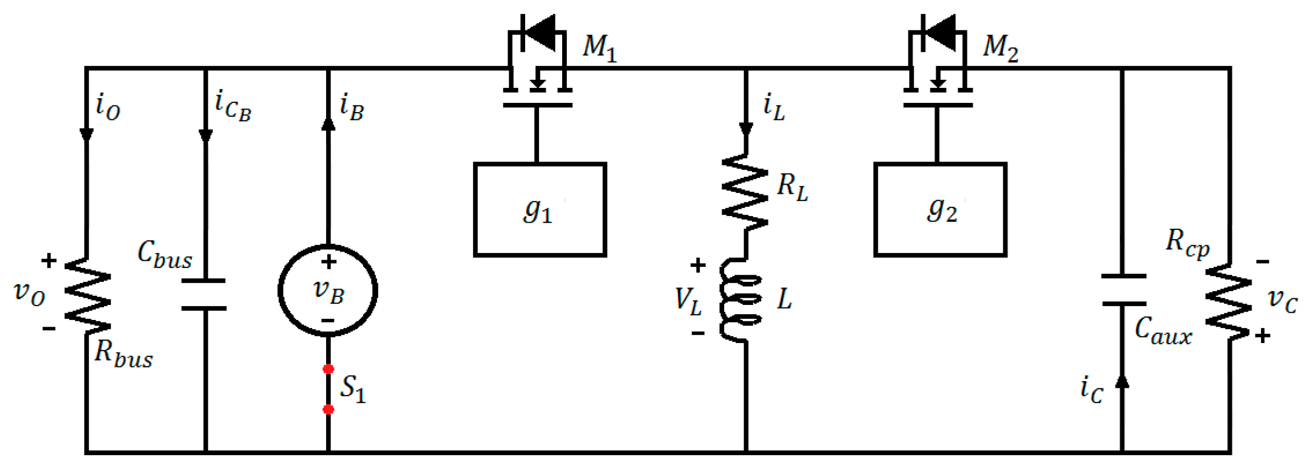
3. Modeling and Control of the BBBC Converter

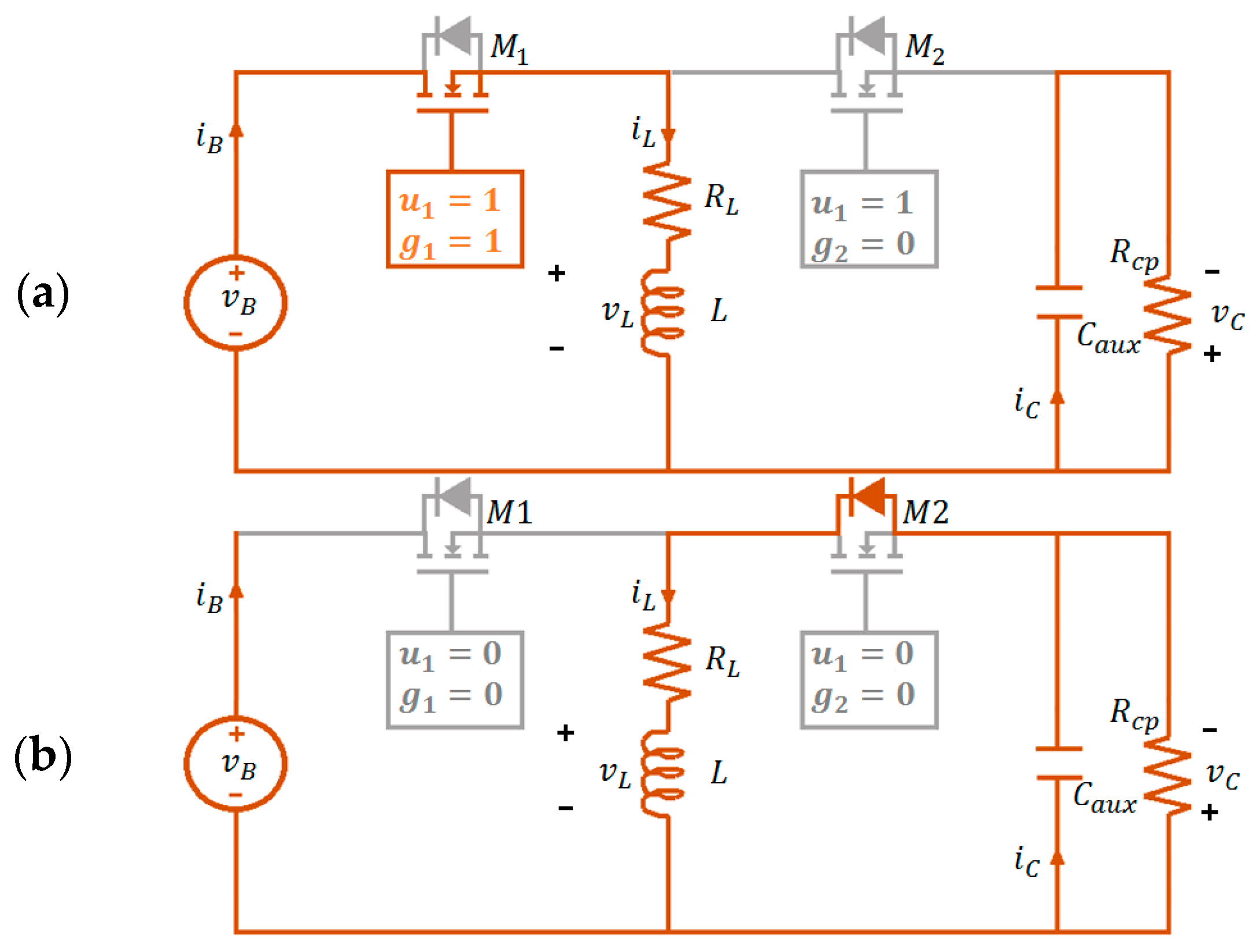
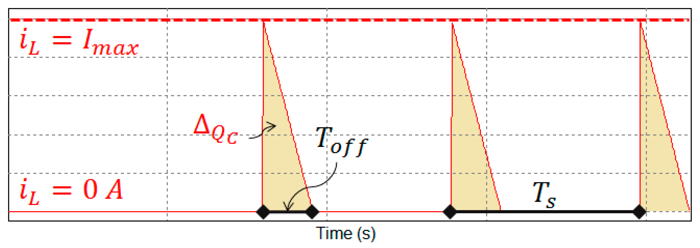
3.1. Capacitor Charging Mode

The two circuit structures of the BBC converter, operating in Continuous Conduction Mode CCM (or BCM), associated with the charging mode, are depicted in Figure 5. In this case, the converter can charge the capacitor, C a u x , by taking energy from the DC bus. This charging process is enforced at a constant-current rate by changing the state of the control switch, M 1 , maintaining switch M 2 off. The variable u 1 is defined in such a way that u 1 = 1 when M 1 is on, and u 1 = 0 when M 1 is off. The intrinsic diode of M 2 is on when M 1 is off.
The nonlinear dynamic behavior of the BBBC converter in this mode can be represented as the bilinear equation system (1).
  L d i L d t = v B u 1 v C ( 1 u 1 ) i L R L   C a u x d v C d t = i L ( 1 u 1 ) v C R c p
Then, operation in BCM can be enforced on the inductor current, setting a hysteresis band with limits at I m a x > 0 and zero, as defined in the following switching law:
  u 1 = { 1                                             i L δ               0                                             i L I m a x          
where δ is a small positive value. Then, the capacitor charges depending on the average value of the current; this means that the charging process is related to the average value of the control signal, u 1 . From conventional sliding-mode analysis [19], the value u 1 a v g denotes the equivalent control signal when the switches at the converter change states are at an infinite frequency, in other words, u 1 a v g represents the average value of the duty cycle (i.e., the control signal as a continuous variable). In the case of the converter operating in BCM [20], due to the triangular shape of the current, it is possible to ensure that the cycle-by-cycle average of the current is half the maximum limit of the current. Then, by defining I r e f = I m a x 2 , S ( x ) = i L I r e f , S ˙ ( x ) = d i L d t and S ( x ) =   S ˙ ( x ) = 0 , from Equation (1), equivalent control Equation (3) can be obtained.
  u 1 a v g = 2 v C + I m a x R L 2 ( v B + v C )                               0 u 1 a v g < 1.
Using Equations (1) and (3), and considering that R c p v C , the ideal dynamic behavior of the average voltage at the capacitor is:
d v C d t = I m a x 4 C a u x ( 2 v B I m a x R L v B + v C ) .
By solving Equation (4), considering v C ( 0 ) = 0 , the instantaneous output voltage is:
v C ( t ) = v B + v B 2 + I m a x ( 2 v B I m a x R L ) 2 C a u x t .
The charge time can be computed by substituting the final value of v C as V C m a x , obtaining:
t a = 2 C a u x I m a x ( V C m a x 2 + 2 V B V C m a x 2 v B I m a x R L ) .

3.2. Stand-By Mode

In this mode, both switches M 1 and M 2 are off. The circuit defining v C ( t ) becomes solely the parallel between C a u x and R c p . Therefore, the dynamic behavior is defined by:
d v C d t + v C R c p C a u x = 0 .
By solving Equation (7), considering v C ( t a ) = V C m a x , the output voltage is obtained as:
  v C ( t ) = V C m a x e ( t   R c p C a u x ) .
The stand-by interval can be computed by substituting the final value of v C as V C n o m , obtaining:
t b = R c p C a u x ln ( V C n o m V C m a x ) .

3.3. Recharging Mode of the Capacitor

During this interval, the circuit operates in charging mode until the capacitor voltage reaches V C m a x again. The behavior of v C can be modelled by analyzing the cycle-by-cycle waveform of the current at capacitor (see Figure 6). It is possible to observe that the contribution of each current pulse on the capacitor’s charge is given by:
Δ Q c = 2 L I m a x 2 2 v C + I m a x R L .
By taking into account Equation (10), it can be deduced that the drop voltage, Δ V c = V C m a x V C n o m , is recovered with N current pulses during a time interval t c defined by:
t c 2 C a u x Δ V c ( V B + V C m a x + V C n o m + I m a x R L ) V B I m a x .

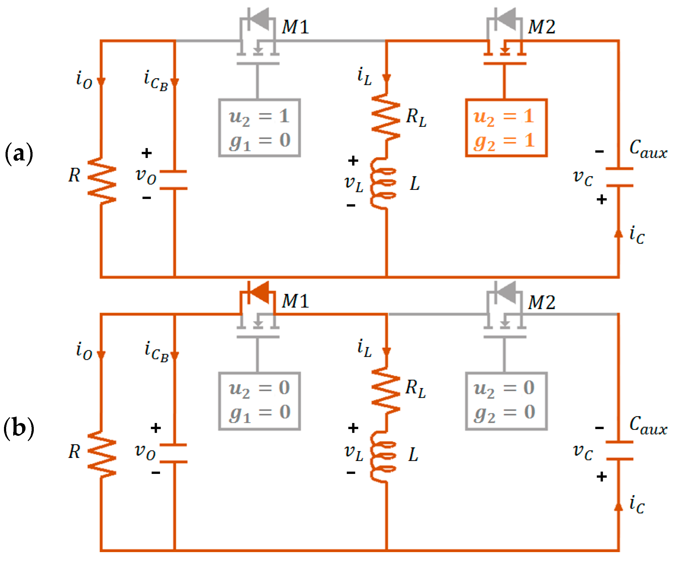
3.4. Discharging Mode of the Capacitor

Figure 7 shows the on and off structures of the BBBC circuit in the discharging mode. In this mode, the energy transfer from the capacitor, C a u x , to the critical load (connected in parallel to capacitor C B ) is accomplished using the converter. For this analysis, R c p is not included because its effect on the dynamic behavior is negligible compared with the load R , which is now connected to the input side of the converter.
By deriving and combining equations for each circuit structure, the following bilinear system of equations is obtained:
  L d i L d t = v C u 2 + v O ( 1 u 2 ) i L R L   C a u x d v C d t = i L u 2 C B d v O d t = v O R i L ( 1 u 2 ) .
Similar to the derivation of Equation (3), we have S ( x ) = i L i r e f , S ˙ ( x ) = d i L d t d i r e f d t and S ( x ) =   S ˙ ( x ) = 0 , then, from Equation (12), the following average control is obtained:
  u 2 a v g = v O L d i r e f d t i r e f R L v O + v C               0 u 2 a v g < 1 ,
obtaining switching law Equation (14).
  u 2 = { 1                       i L γ           0                       i L i max d c h      
where γ is a small positive value. From Equations (12) and (13), the ideal dynamic behavior of the average voltage at the capacitors is:
  C a u x d v c d t = i r e f ( v O L d i r e f d t i r e f R L v O + v C ) C B d v O d t = v O R i r e f ( v C + L d i r e f d t i r e f R L v C + v O ) .
By combining the two expressions in Equation (15), the following linear Equation (16) is derived.
C B d v O d t = v O R i r e f + C a u x d v c d t .
In the discharge mode, an outer voltage controller will enforce v O = V O by means of the reference current, i r e f . The cycle-by-cycle average current can be derived by imposing zero dynamics in Equation (12) obtaining i r e f = V O R V O 2 R v c . Then, substituting this expression in Equation (16), the dynamic behavior of v c is:
d v C d t + V O 2 R C a u x v C = 0 .
By solving Equation (17), considering v C ( 0 ) V C m a x , the instantaneous output voltage is:
v C ( t ) = V C m a x 2 2 V O 2 R C a u x t .
The discharge interval can be computed by substituting the final value of v C as V C m i n , obtaining:
t d = R C a u x 2 ( V C m a x 2 V C m i n 2 V O 2 ) .
Regulation of the voltage at the bus can be accomplished by using a simple proportional-integral (PI) controller. The transfer function of the current-controlled converter can be obtained from the Laplace transform of Equation (16). The reference current, i r e f , has been replaced by i m a x / 2 since this value defines the average value of the current on the inductor i L .
V O ( s ) = I m a x ( s ) 1 2 C b s + 1 R C b G i v ( s ) + V C ( s ) C C b s + 1 R C b G v v ( s ) .
In Equation (20) the voltage V C ( s ) must be considered as a disturbance; then, assuming its value as zero, the DC bus voltage is obtained for a maximum-current transfer function. Then, the output voltage can be indirectly regulated by configuring a nested loop architecture in which the outer controller regulating the output voltage gives the reference of the inner current loop [21,22]. By defining the PI controller transfer function in the classical way, we have:
C ( s ) = K p s + K i s .
The parameters of Equation (21) can be computed by applying any classical design method, such as frequency-response, root-locus or advanced-control methods, especially methods that allow a robust response to the changes in operation point (i.e., the use of the instantaneous voltage from the auxiliary capacitor) with uncertainty about the parameters (e.g., power consumption of the critical load) [22]. Regardless of the method, the closed-loop transfer function is:
V O ( s ) V r e f ( s ) = K p s + K i 2 C b s 2 + 1 C b ( 1 2 R + K p ) s + K i 2 C b .

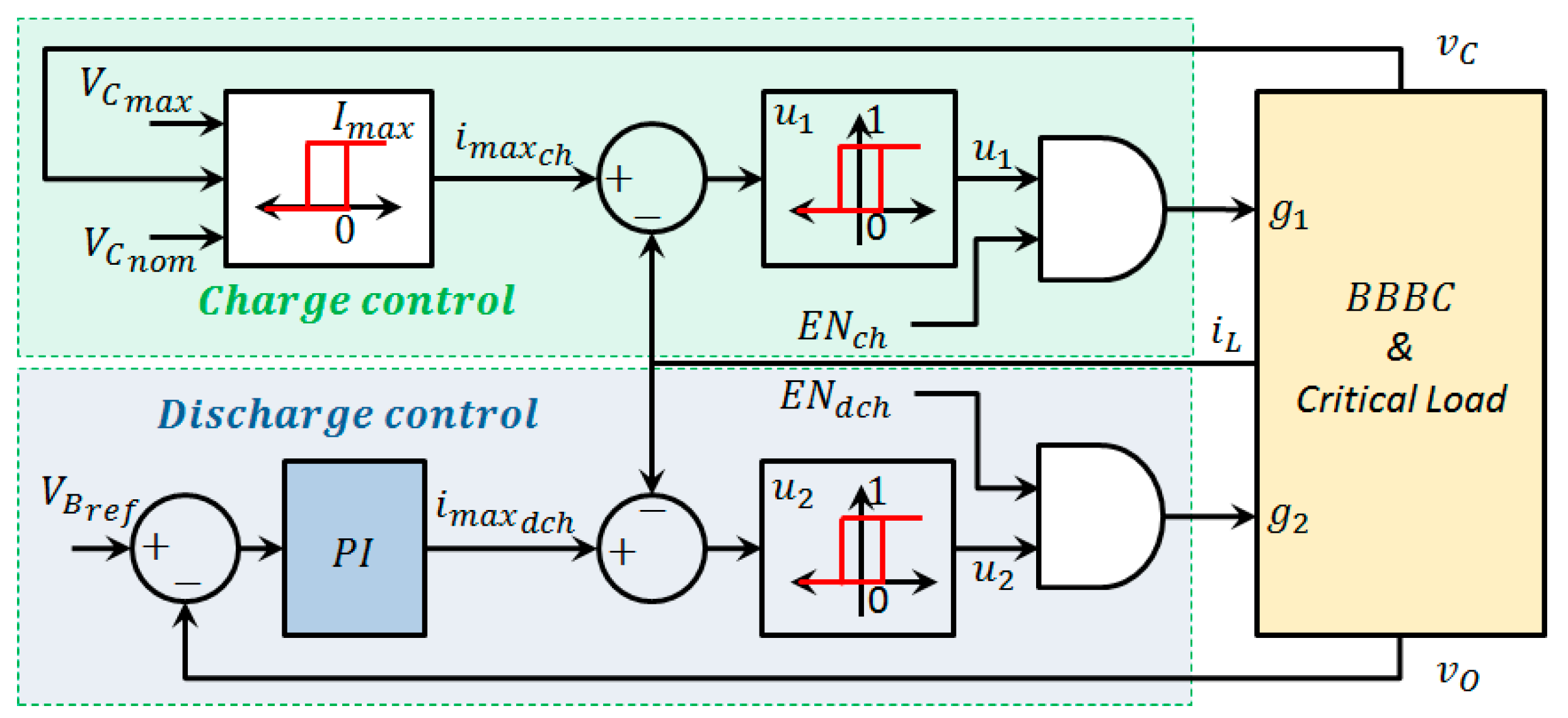
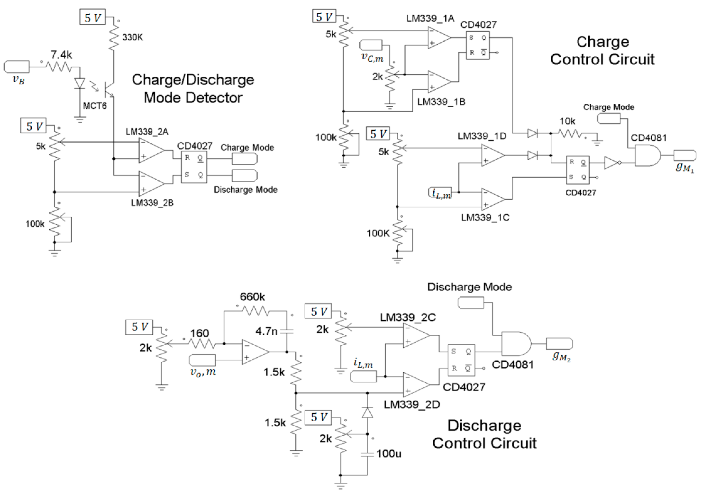
3.5. Complete Control Diagram

To clarify the implementation of the proposed control module, the block diagram in Figure 8 is presented. In this figure, we have separated the control of the charge from the discharge control since the two control sub-modules have slight differences. Both the charge and discharge control modules have a hysteresis comparator to force the inductor current to operate in BCM, which corresponds to the switching laws in Equations (2) and (14), respectively. The control signals u 1 and u 2 , which are given by the inner current controllers, are also conditioned to the existence of enabling signals, provided by the mode-selection logic described in Figure 3. In the case of the charge control, the nonlinear outer loop of voltage regulation constitutes a nested loop or cascade control architecture (together with the hysteresis comparator). This controller corresponds to definitions given in Section 3.2 and Section 3.3. The output of the outer loop defines whether the maximum value of the current is the I m a x value configured by the user or zero, deactivating the inner loop. In the case of the discharge control, also a nested loop is used, in which the PI controller defined in Equation (21) gives the reference for the current controller in order to regulate the input voltage of the critical load. Details of the circuit implementation are given in the results section.

3.6. Converter Design Parameters

Operation of the converter in BCM implies a variable switching frequency. Then, the inductor of the converter must be designed considering the extreme cases. In order to determine the range of switching frequencies during the charge mode, the on and off time intervals are determined as:
  T o n = L | I m a x V B |                                                 V B > 0 T o f f = L | I m a x V C |                                               V C > 0 .
The switching period can be obtained as T s = T o n + T o f f , and hence, the switching frequency can be derived. The singularity of V C = 0 appears only at the start of the charge interval. In that case, T o f f is equal to zero because there is no change for the inductor current.
f s = 1 T s = v C v B L I m a x ( v B + v O ) .
Notice that the per-cycle value of the frequency depends on the capacitor’s voltage, which varies during the charging process. Therefore, the range of the switching frequency is defined by the value of the inductance. The auxiliary capacitor is designed depending on the extension required in the hold-up time. Capacitance is determined to ensure a defined amount of stored energy to be delivered in order to support the momentary power failures. Considering a load connected to the DC bus with a power consumption of P and a desired autonomy time of t d , the value of the required capacitance can be computed as:
  C a u x = 2   P   t d η ( V C m a x 2 V C m i n 2 )   ,
where η represents the efficiency of the HTEC. This value can be related to the losses in the power converter, which in fact depend on the operation point and the critical load consumption. A good choice for this value can be the minimum converter efficiency that always satisfies t d . Converter efficiency as a function of the operation point of the converter can be experimentally determined by applying a test bench of controlled variation in the voltage of the capacitor and the load power.

4. Simulation and Experimental Results

First, to validate the correct operation of the proposed circuitry and control module, several simulation runs were conducted using the PSIM software package. The parameters of the simulation are listed in Table 1.

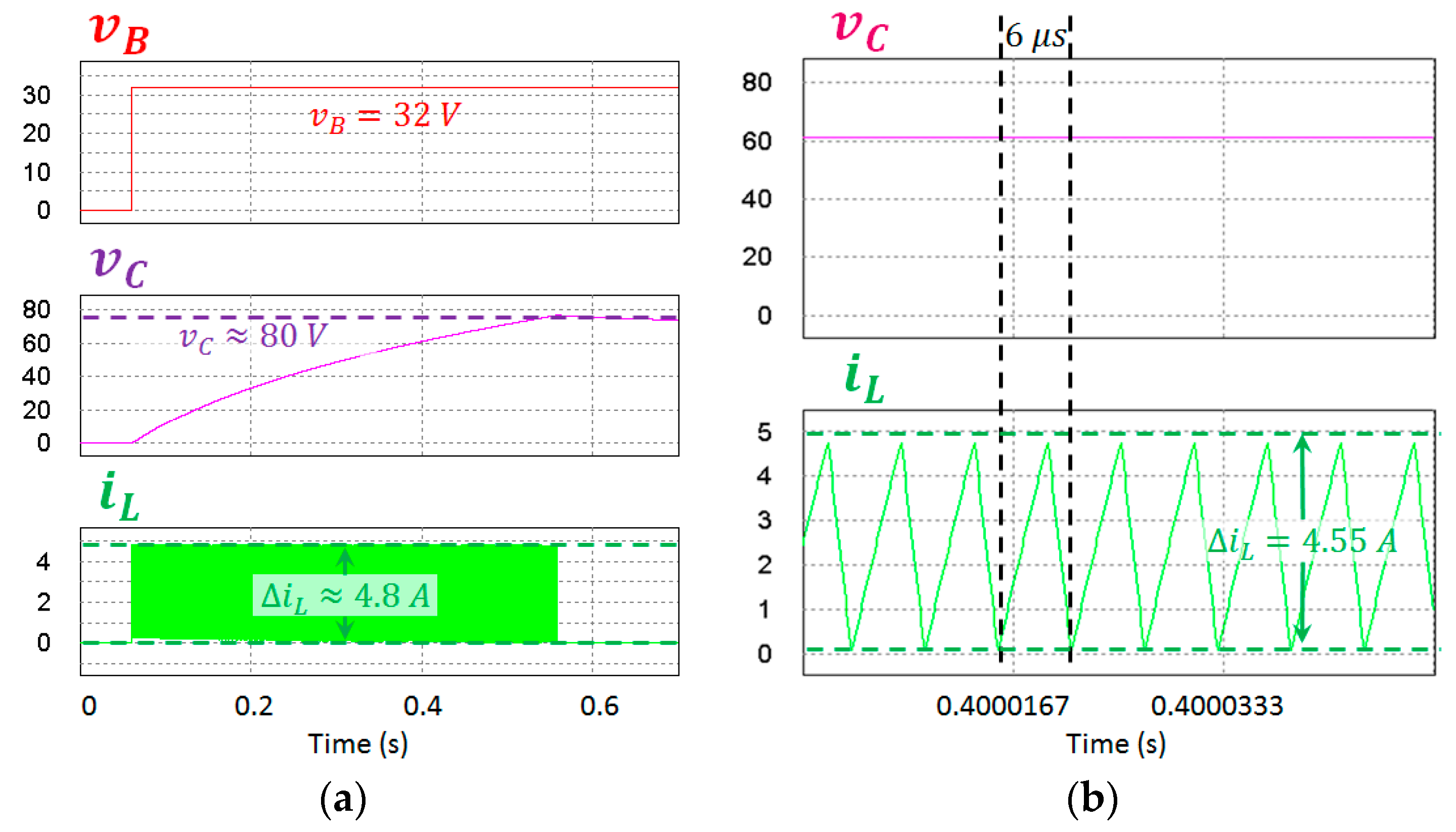
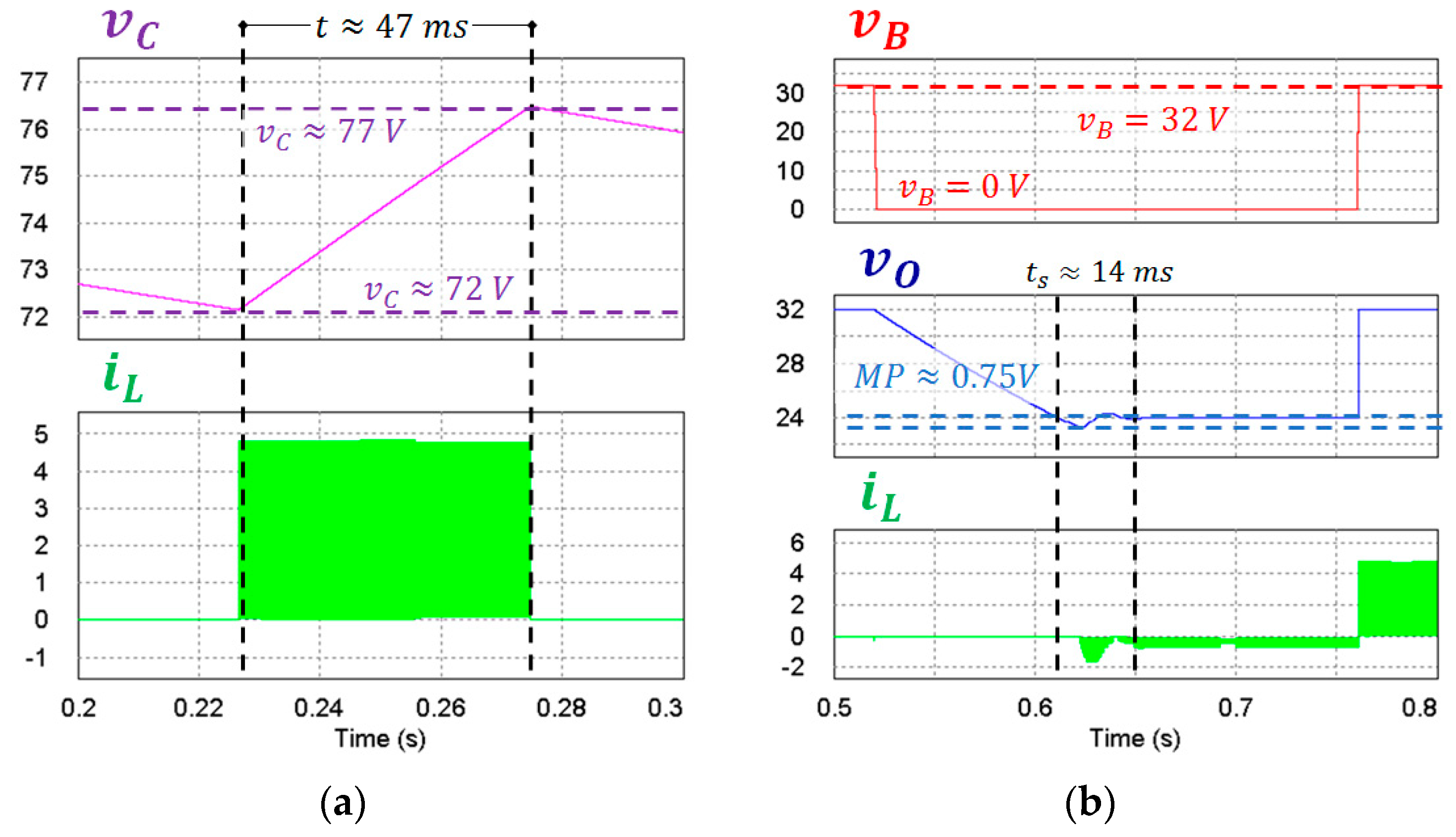
4.1. Simulation Results

In Figure 9, the system starts in off-line mode until it enters in the charge mode at 0.75 s when the capacitor begins charging at 75 V using pulse-wise current limited between zero and the defined maximum value (5 A). In the second interval (stand-by mode), the capacitor’s voltage decreased due to the self-discharge resistance (since the real self-discharge resistance was very high, a resistance of 1 kΩ was used to reduce the duration of this interval). Once the capacitor voltage fell out of the hysteresis band (its value decreased below 73 V), the charge mode was reactivated again to recover the voltage level. After that, a bus failure was introduced at 0.35 s; the bus capacitor discharged first down to the voltage level programmed to activate the operation in the discharge mode. After that, the circuit entered a discharging mode regulating the bus voltage to a reference value of 24 V.
A detail of the first charging mode interval in Figure 9 is depicted in Figure 10a for a test with a reduced interval in off-line mode. As shown in the figure, the entire interval had an approximate duration of 500 ms, during which switching frequency increased from 2.6 to 200 kHz, staying at around 150 kHz for most of the charging interval. Figure 10b shows the period of the current signal at around 0.4 s when the charging voltage was close to its final value; this corresponded to a switching frequency of 166 kHz. For these results it is worth considering that an additional resistor of 1 kΩ must be also be fed during the charging mode, increasing the complete charging time interval. Approximately at 0.55 s, the system entered stand-by mode and the inner commutation was switched off.
Figure 11a details the charging mode in which the system entered after a stand-by interval. In this case, some current pulses were required to recover the voltage level in the capacitor, avoiding prolonged self-discharge. For this test, it is important to mention that a mean value of 74.5 V was established in the auxiliary capacitor through a hysteresis band defined between 72 and 77 V. In Figure 11b, the detail of a bus failure can be observed. The voltage of the bus fell to zero at 0.52 s, then, after disconnecting the load from the bus, the voltage decreased until reaching the limit of 24 V defined to activate the discharging mode. A short and almost imperceptible transient state was observed between 0.61 and 0.65 s when the voltage was regulated, maintaining the conditions until the bus recovered an acceptable voltage level to operate at 0.72 s.

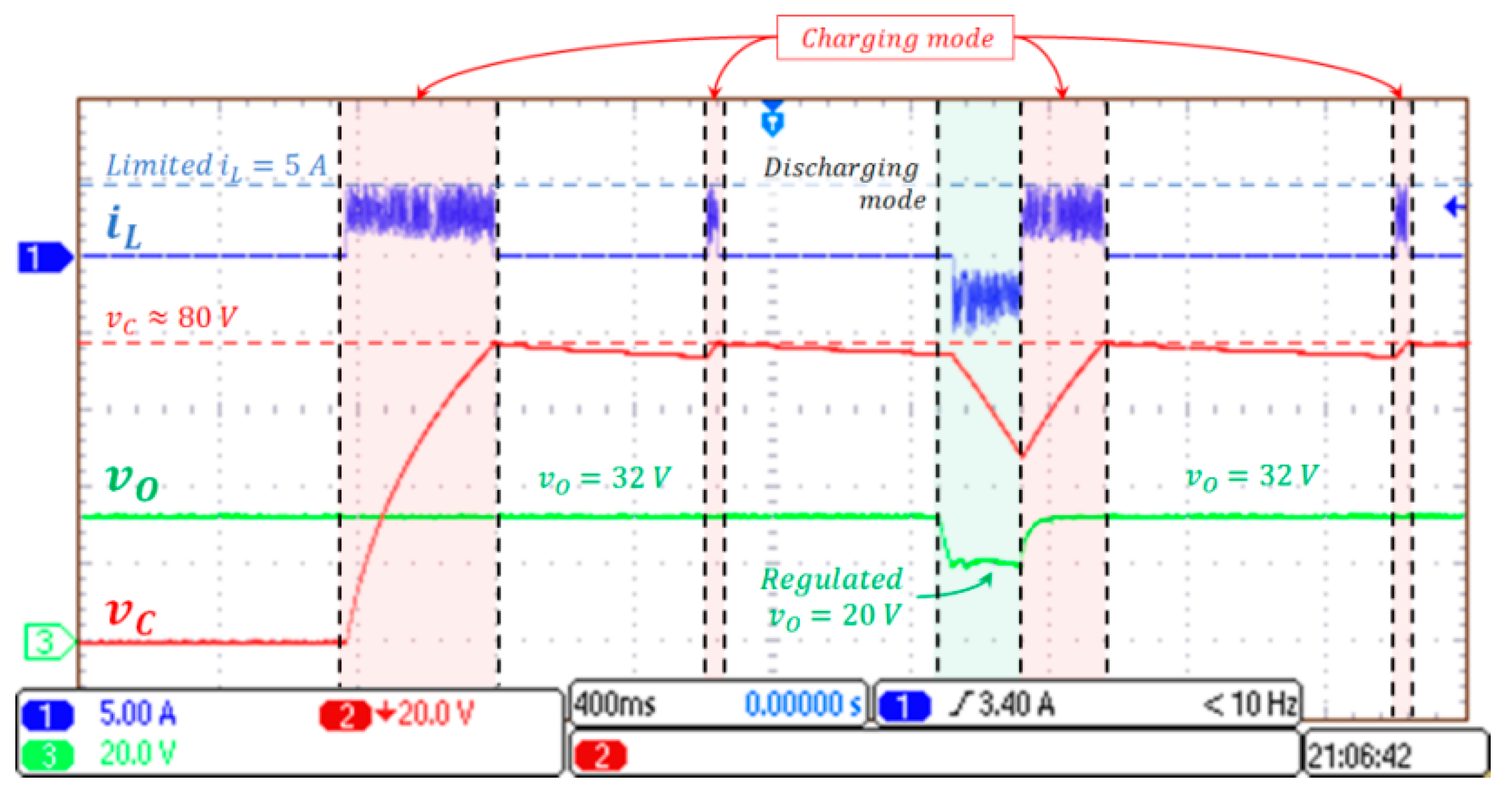
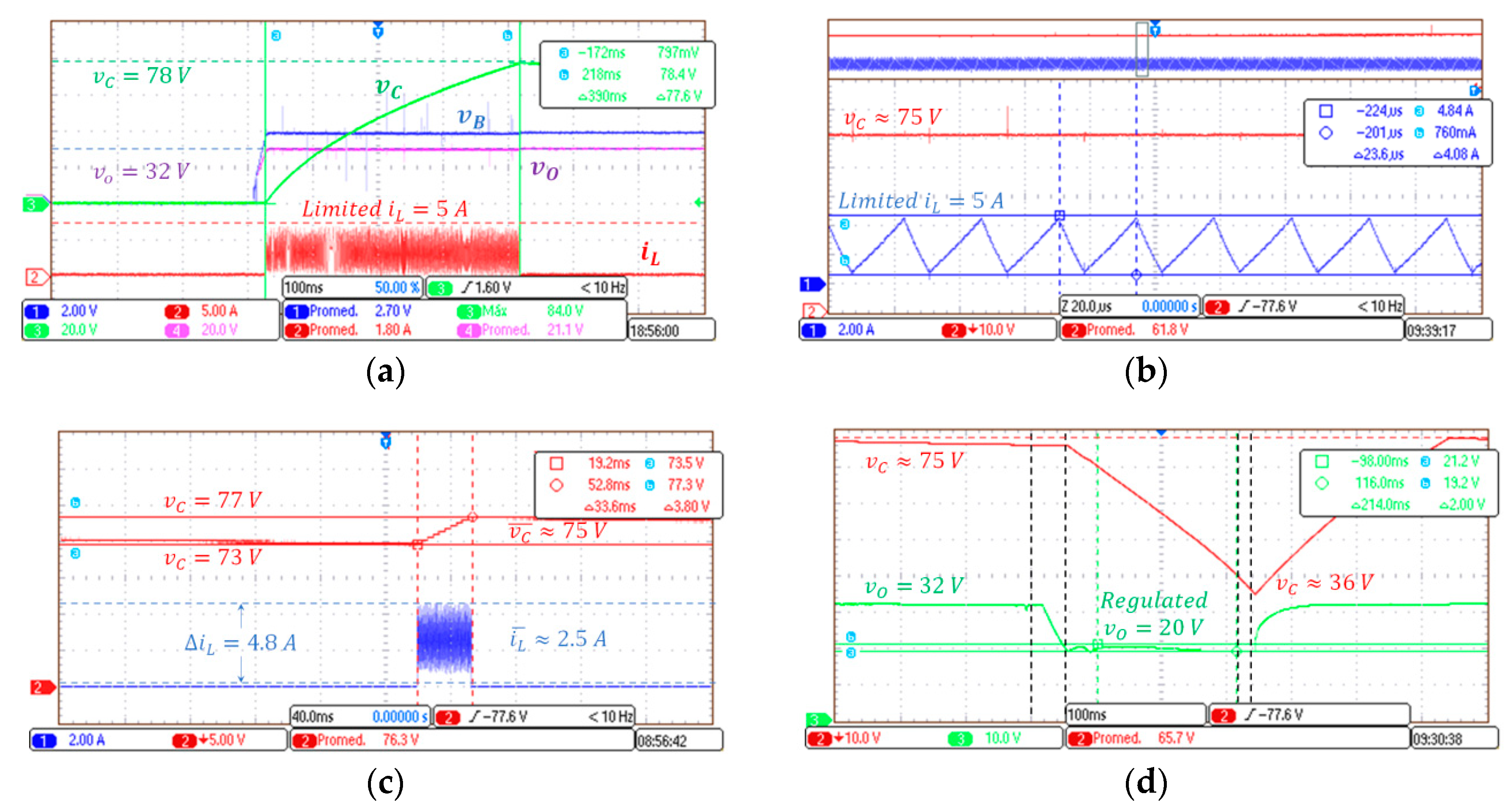
4.2. Experimental Results

A prototype of the proposed system was built to provide the experimental results. The power module was built using the converter parameters in Table 1, two AOTF15S60 MOSFET (Alpha & Omega Semiconductor, CA, USA), and one opto-isolated driver TLP350 (Toshiba Corporation, Tokyo, Japan). The bus capacitance and auxiliary capacitance were built by paralleling four 470 µF/100 V capacitors and six 100 µF/160 V capacitors, respectively. An additional resistor of 1 kΩ in parallel with the auxiliary capacitor was added to emphasize the effect of the self-discharging resistance and facilitate signal capture, evaluating the entire behavior of the circuit. As sensors, two isolated closed-loop hall-effect transducers LV-20P (LEM International SA, Ginebra, Switzerland) were used to measure the bus voltage and the auxiliary capacitor voltage; one isolated closed-loop hall-effect transducer CAS 15-NP (LEM International SA, Ginebra, Switzerland) was used to measure the inductor current. These sensors were selected to provide a reliable and accurate validation of the control proposal. However, for implementation of the systems in a commercial product, these elements can be replaced by low cost circuits. The control circuit depicted in Figure 12 was built using LM319 comparators, LM347 operational amplifiers (Freescale Semiconductors, TX, USA), and CD4027 flip-flops (Texas Instruments, TX, USA).
The experimental set-up was composed of a Mixed Signal Digital Oscilloscope MSO2014B equipped with an isolated current probe TCP0020 (Tektronix, OR, USA) and three isolated voltage probes. Figure 13 shows an oscilloscope capture of the circuit variables during a test, evaluating its entire functionality. Overall, the circuit operated as expected, in line with the simulation results. To detail the results for each operation mode, Figure 14a shows the charging mode coming from the off-line mode, while Figure 14c details the charging mode coming from the stand-by mode. In Figure 14b, the charging mode is detailed at the switching frequency level to show the current waveform associated with the converter operating in BCM. Finally, Figure 14d details the discharging mode, illustrating the performance of the bus regulation control module while the auxiliary capacitor is discharging.
As shown in all captures in Figure 14, the behavior of the real HTEC agrees with the simulation results and the theoretical analysis. Current regulation in the two modes was accomplished and external voltage control was equally effective, obtaining the hysteretic behavior for the auxiliary capacitor, which prevents the undesired switching of the converter and limits the recharging process of the capacitor to short intervals. Although the recharging interval was close to 4 ms (in measurements), it is worth pointing out that this value was related to the additional resistor used to reduce the stand-by time, which was included to obtain the comprehensive graphic capture of the circuit operation depicted in Figure 13. Regulation of the bus was really effective because no overshoot was present and the steady-state error was limited to ±1 V around the reference value.

5. Conclusions

An improved-control approach for the parallel HTEC, based on the BBBC operating in BCM, has been proposed and described in detail. The developed control module stands out for its simplicity, robustness and reliability. Every operational mode of the converter has been modelled, obtaining a comprehensive set of expressions to analyze the behavior of the circuit and facilitate its design. Both simulation and experimental results confirmed the validity of the approach and its potential use in real applications. Current efforts towards improving the HTEC are focused on the digital implementation of the control module in a microcontroller with an analog comparator module, which promises to enhance the performance of the system without losing precision or simplicity due to discretization. The experimental validation of this new approach will include optimization of the components and the Printed Circuit Board area.

Author Contributions

Conceptualization, O.L.-S. and J.O.U.-A.; formal analysis, O.L.-S.; funding acquisition, O.L.-S.; investigation, O.L.-S., J.O.U.-A., S.T.-L. and J.D.A.-L.; methodology, O.L.-S.; project administration, O.L.-S.; validation, O.L.-S., S.T.-L. and J.D.A.-L.; writing—original draft, O.L.-S. and S.T.-L.; writing—Review and editing, O.L.-S. and J.O.U.-A.

Funding

This research was developed with the partial support of the Gobernación del Tolima under Convenio de cooperación 1026-2013 and the Universidad de Ibagué under project 16-435-SEM. The APC was funded partially by Universidad de Ibagué.

Conflicts of Interest

The authors declare no conflicts of interest.

References

  1. Guidance for Test Procedures for Demonstration of Utilization Equipment Compliance to Aircraft Electrical Power Characteristics 28VDC, Department of Defense Handbook, 2004. Available online: http://everyspec.com/MIL-HDBK/MIL-HDBK-0700-0799/MIL-HDBK-704-8_14620/ (accessed on 8 February 2018).
  2. Radio-Technical Commission for Aeronautics (RTCA). DO-160, Environmental Conditions and Test Procedures for Airborne Equipment; Section 16, Power Input ED-14G; RTCA: Washington, DC, USA, 2011. [Google Scholar]
  3. IEEE 946-2004. Recommended Practice for the Design of DC Auxiliary Power Systems for Generating Systems; IEEE Std 946-2004: New York, NY, USA, 2004. [Google Scholar]
  4. IET Standards. Code of Practice for Low and Extra Low Voltage Direct Current Power Distribution in Buildings; IET Standards: Stevenage, UK, 2015; pp. 1–60. [Google Scholar]
  5. ST Microelectronics. Power Supply Hold-up Time; TN0024 Technical Note; ST Microelectronics: Santa Clara, CA, USA, 2007; pp. 1–11. [Google Scholar]
  6. Jin, X.; Lin, H.; Yao, W.; Deng, Y.; Lyu, Z.; Qian, B. Hold-up time extension method for forward converter. In Proceedings of the IEEE 2nd Annual Southern Power Electronics Conference (SPEC), Auckland, New Zealand, 5–8 December 2016; pp. 1–4. [Google Scholar]
  7. Jang, Y.; Jovanovic, M.; Dillman, D.L. Hold-up time extension circuit with integrated magnetics. IEEE Trans. Power Electron. 2006, 21, 394–400. [Google Scholar] [CrossRef]
  8. Jang, Y.; Jovanovic, M. Hold-up-Time Extension Circuits. U.S. Patent No. US20020071300A1, 13 June 2002. [Google Scholar]
  9. Liu, G.; He, L. Hold-up Time Extension Circuit for a Power Converter. U.S. Patent No US20130027981A1, 31 January 2013. [Google Scholar]
  10. Wang, H.; Liu, W.; Chung, H. Hold-up time analysis of a dc-link module with a series voltage compensator. In Proceedings of the IEEE Energy Conversion Congress and Exposition (ECCE), Raleigh, NC, USA, 15–20 September 2012; pp. 1095–1100. [Google Scholar]
  11. Picard, J. High-Voltage Energy Storage: The Key to Efficient Holdup; Texas Instruments: Dallas, TX, USA, 2008. [Google Scholar]
  12. Interpoint. HUM-40, HUM-70, Interpoint’s Hummer Hold-Up Module Series. 2009, pp. 1–13. Available online: http://www.interpoint.com/product_documents/HUM70_Hold_Up_Module_DC_DC.pdf (accessed on 8 February 2018).
  13. Gaïa Converter. Hi-Rel Hold-up module HUGD-50: 50 Power. 2014, pp. 1–13. Available online: http://gaia-converter.com/50-watt-hugd-50 (accessed on 8 February 2018).
  14. Lai, C.-M.; Li, Y.-H.; Cheng, Y.-H.; Teh, J. A High-Gain Reflex-Based Bidirectional DC Charger with Efficient Energy Recycling for Low-Voltage Battery Charging-Discharging Power Control. Energies 2018, 11, 623. [Google Scholar] [CrossRef]
  15. Shiau, J.-K.; Ma, C.-W. Li-Ion Battery Charging with a Buck-Boost Power Converter for a Solar Powered Battery Management System. Energies 2013, 6, 1669–1699. [Google Scholar] [CrossRef] [Green Version]
  16. Serna-Garcés, S.I.; Gonzalez Montoya, D.; Ramos-Paja, C.A. Sliding-Mode Control of a Charger/Discharger DC/DC Converter for DC-Bus Regulation in Renewable Power Systems. Energies 2016, 9, 245. [Google Scholar] [CrossRef]
  17. Ramos-Paja, C.A.; Bastidas-Rodríguez, J.D.; González, D.; Acevedo, S.; Peláez-Restrepo, J. Design and Control of a Buck–Boost Charger-Discharger for DC-Bus Regulation in Microgrids. Energies 2017, 10, 1847. [Google Scholar] [CrossRef]
  18. Lopez-Santos, O.; Urrego-Aponte, J.O.; Almansa-López, J.D. Modeling and control of a new circuit to obtain hold-up time extension for electronic equipment in aircraft applications. In Proceedings of the 2016 International Conference on Electrical Systems for Aircraft, Railway, Ship Propulsion and Road Vehicles & International Transportation Electrification Conference (ESARS-ITEC), Toulouse, France, 2–4 November 2016; pp. 1–7. [Google Scholar]
  19. Flores-Bahamonde, F.; Valderrama-Blavi, H.; Bosque-Moncusi, J.M.; García, G.; Martínez-Salamero, L. Using the sliding-mode control approach for analysis and design of the boost inverter. IET Power Electron. 2016, 9, 1625–1634. [Google Scholar] [CrossRef]
  20. Chen, J.; Erickson, R.; Maksimovic, D. Averaged switch modeling of boundary conduction mode DC-to-DC converters. In Proceedings of the 27th Annual Conference of the IEEE Industrial Electronics Society (IECON), Denver, CO, USA, 29 November–2 December 2001; Volume 2, pp. 844–849. [Google Scholar]
  21. Lopez-Santos, O.; Zambrano-Prada, D.A.; Aldana-Rodriguez, Y.A.; Esquivel-Cabeza, H.A.; Garcia, G.; Martinez-Salamero, L. Control of a Bidirectional Cûk Converter Providing Charge/Discharge of a Battery Array Integrated in DC Buses of Microgrids. Commun. Comput. Inf. Sci. 2017, 742, 495–507. [Google Scholar]
  22. Lopez-Santos, O.; Martinez-Salamero, L.; Garcia, G.; Valderrama-Blavi, H.; Sierra-Polanco, T. Robust Sliding-Mode Control Design for a Voltage Regulated Quadratic Boost Converter. IEEE Trans. Power Electron. 2015, 30, 2313–2327. [Google Scholar] [CrossRef]
Figure 1. Block diagram representing application context of proposed hold-up time extension circuit (HTEC) in an Extra Low Voltage DC (ELVDC) bus.
Energies 11 02560 g001
Figure 2. Block diagram representing proposed HTEC, ELVDC bus and critical load.
Energies 11 02560 g002
Figure 3. Schematic circuit model of the bidirectional buck-boost converter.
Energies 11 02560 g003
Figure 4. Event based diagram defining control modes and transition events.
Energies 11 02560 g004
Figure 5. Circuit structures of the Bidirectional Buck-Boost Converter (BBBC) during the charging mode operation. (a) Control switch on; (b) control switch off.
Energies 11 02560 g005
Figure 6. Current on the capacitor C m a x during recharge mode.
Energies 11 02560 g006
Figure 7. Circuit structures of the BBBC in the discharging mode. (a) Control switch on; (b) control switch off.
Energies 11 02560 g007
Figure 8. Block diagram of the proposed control for the HTEC based on the BBBC.
Energies 11 02560 g008
Figure 9. Simulation results showing waveforms for all operational modes of the proposed HTEC.
Energies 11 02560 g009
Figure 10. Simulation results detailing charging mode. (a) Details of the auxiliary capacitor voltage; (b) details of the inductor current.
Energies 11 02560 g010
Figure 11. Detailed simulation results. (a) Auxiliary capacitor voltage during the recharging mode; (b) ELVDC bus voltage during discharging mode.
Energies 11 02560 g011
Figure 12. Schematic circuit diagram of the proposed control for the HTEC.
Energies 11 02560 g012
Figure 13. Oscilloscope capture showing all operation modes of the HTEC.
Energies 11 02560 g013
Figure 14. Detailed experimental results. (a) Charging mode and standby mode; (b) details of the inductor current during charging mode; (c) standby mode and recharging mode; (d) discharging mode.
Energies 11 02560 g014
Table 1. Specifications and parameters of the studied HTEC.
General Operation SpecificationsConverter Parameters
ParameterSymbolValueUnitsParameterSymbolValueUnits
Nominal bus voltage V B n o m 28VBus capacitor C B 1.880µF
Maximum bus voltage V B m a x 36VAuxiliary capacitor C a u x 600µF
Minimum bus voltage V B m i n 22VSelf-discharge capacitor resistance R c p 1kΩ
Regulated bus voltage V B r e f 20VInductor L 25µH
Auxiliary capacitor max. voltage V C m a x 78VBus load resistance R 12
Auxiliary capacitor nom. voltage V C n o m 73VDischarge PI Regulator Parameters
ParameterSymbolValue
Auxiliary capacitor min. voltage V C m i n 12VProportional gain (Discharge) K p 15
Maximum charge current I m a x 10AIntegral gain (Discharge) K i 5.000

