Article

Design and Control of a 13.2 kV/10 kVA Single-Phase Solid-State-Transformer with 1.7 kV SiC Devices

1
Department of Electrical Engineering, Konkuk University, Seoul 05029, Korea
2
Department of Control and Instrumentation Engineering, Korea University of Transportation, Chungju 27469, Korea
*
Author to whom correspondence should be addressed.
Energies 2018, 11(1), 201; https://doi.org/10.3390/en11010201
Submission received: 8 December 2017 / Revised: 11 January 2018 / Accepted: 12 January 2018 / Published: 15 January 2018
(This article belongs to the Section F: Electrical Engineering)

Abstract

:
This paper describes the power stage design, control, and performance evaluation of a 13.2 kV/10 kVA solid-state-transformer (SST) for a power distribution system. The proposed SST consists of 10 modules where each individual module contains a unidirectional three-level power factor correction (PFC) converter for the active-front-end (AFE) stage and an LLC resonant converter for the isolated DC-DC stage. The operating principles of the converters are analyzed and the modulation and the control schemes for the entire module are described in detail. The DC-link voltage imbalance is also less than other SST topologies due to the low number of uncontrollable switching states. In order to simplify the control of the power stage, a modulation strategy for the AFE stage is proposed, and the modulation frequency of the LLC converter is also fixed. In addition, a compensation algorithm is suggested to eliminate the current measurement offset in the AFE stage. The proposed SST achieves the unity power factor at the input AC current regardless of the reactive or nonlinear load and a low voltage regulation at the AC output. In order to verify the effectiveness of the SST, the 13.2 kV/10 kV SST prototype is built and tested. Both the simulation and the experimental results under actual 13.2 kV line show the excellent performance of the proposed SST scheme.

1. Introduction

Recently, solid-state-transformers (SSTs) have emerged in the electricity industries where new technologies such as the smart grid, the renewable energies, and the DC distribution systems are adopted [1,2,3,4,5,6]. A SST is a power transformer, which is based on power electronics technology, so that the voltage and the current of the primary and the secondary sides can be actively compensated or controlled which cannot be realized in traditional power transformers. Among various stages in a power system including the generation, the transmission and the substation, and the distribution systems, the power transformers in distribution stages are good candidates to be replaced with SSTs because they are directly connected to the loads, and have relatively lower input voltage compared to the one in the other stages.
Figure 1 compares the structures of a traditional distribution power transformer and a SST configuration. In the Republic of Korea, the primary and the secondary voltages of power distribution stages are standardized as 13.2 kV and 220 V in root-mean-square (rms) value. It means a SST in the distribution stage should be able to operate in the input and the output voltage ranges. Unlike the traditional transformers, the SST consists of three individual power stages, the active-front-end (AFE), the isolated DC-DC, and the load inverter stages. The main roles of each stage are described as follows. First, the AFE converter performs the input power factor correction (PFC) with low total harmonic distortion (THD) as well as regulating the input DC voltage of the isolated DC-DC stage. It means that the utility grid can treat the SST as a purely resistive load, which does not produce harmonics. Since the unity power factor (PF) can be achieved, only a real power is transferred from the power system to the load regardless of the characteristics of the load. This is an important merit of the SST regarding the power system, because no reactive power is supplied. In fact, it is also possible to supply a reactive power according to the topology selection of the SST. Second, the load inverter stage exists to supply a regulated output voltage. The load inverter employs the DC-link capacitors so that a voltage sag or a short period of an under-voltage fault on the primary sides does not degrade the quality of the output voltage. Furthermore, the load voltage can be easily adjusted when the utility grid is necessary the feature. If a DC distribution is required in the utility grid, the load inverter can be omitted or replaced with a DC-DC converter. Third, the isolated DC-DC stage is employed to offer electrical isolations between the power grid and the load stages. Its input and output voltages are 25 kV and 500 V in this paper, respectively. By combining all three power stages, the SST features very attractive functions as summarized in Table 1.
Regarding SSTs, many research has been conducted. In [7,8,9,10,11,12], SSTs named intelligent universal transformer (IUT), smart transformer (ST), and power electronics transformer (PET), for the medium voltage systems were proposed and tested. In the documents, the neutral point clamp (NPC) type AFE and isolated DC-DC converters were implemented for 2.4 kV AC line. The excellent performance of the SST under the voltage sag and the nonlinear load conditions were demonstrated [8]. In [9], the frequency adaptive repetitive controller is studied for the solid state transformer to interface medium voltage (MV) to low voltage (LV) distribution line, where the operating frequency is varied. The voltage and power balance control methods were presented in [13,14,15] where the cascaded AFE and dual-active-bridge (DAB) converters with all H-bridge modules were employed. Reference [16] discussed the design strategy of the efficient and reliable silicon carbide (SiC) based DC-DC converter for ST. The design of PETs for electric traction applications are dealt in [17,18]. The SSTs for the DC distribution system were described in [4,19]. In [4], the DC droop control strategy was presented, so that the usefulness of the SST in the DC distribution system could be advanced. The 3D space modulation technique of the cascaded converter was proposed in [2]. By using the method, the current and the voltage control performances of the AFE stage could be improved. Reference [20] presented a 15-kV class SST. In the paper, the authors have employed 1.2 kV SiC metal oxide semiconductor field effect transistors (MOSFETs) to the individual power stage to secure high efficiency. Some papers [21,22,23,24,25] have dealt with the SSTs using high voltage switching devices whose voltage rating is over 10 kV. If such high voltage devices become more common, it is expected that the use of SSTs in the power grid can be dramatically increased.
In this paper, a single-phase 10 kVA SST is proposed for the 13.2 kV/220 V power distribution system with 1.7 kV SiC MOSFETs. The proposed SST consists of 10 modules whose voltage rating is 1.32 kV. Each module is composed of a unidirectional three-level PFC converter for the AFE stage and an LLC resonant converter for the isolated DC-DC stage. Compared to other SSTs, where a bidirectional three-level inverter is employed, the proposed AFE stage is simple and reliable. The DC-link voltage imbalance is less than others, because the uncontrollable switching states are much less than them, and no significant power imbalance problem has occurred. The control and modulation are also simple in the proposed AFE and LLC stages. The operations of the individual and total power stage are described in detail. Furthermore, the current offset compensation algorithm for the current measurement offset in the AFE stage is proposed. By using the proposed offset compensation algorithm, the input current offset can be effectively compensated. The simulation and the experimental results show that the excellent current and voltage regulation performance of the proposed SST in practical 13.2 kV power distribution system.

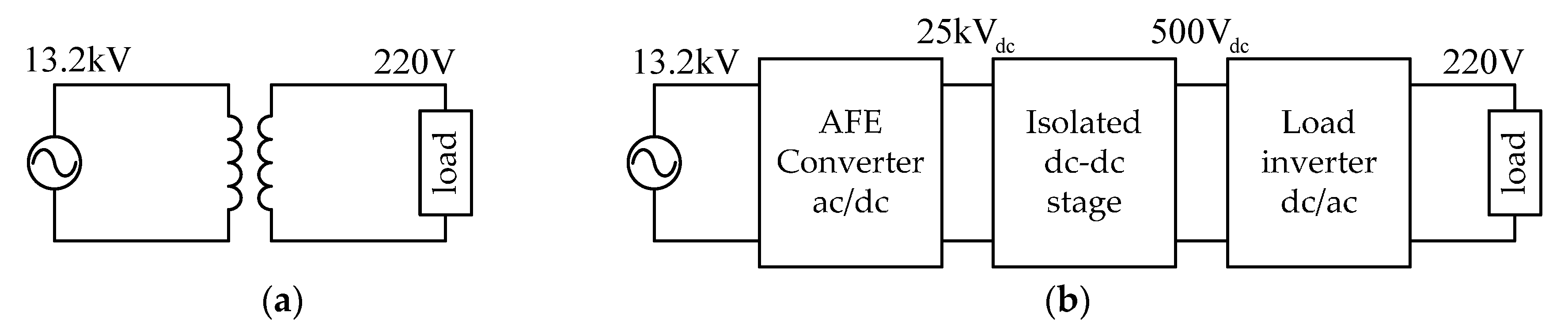
2. Solid-State-Transformer for Electric Power Distribution System

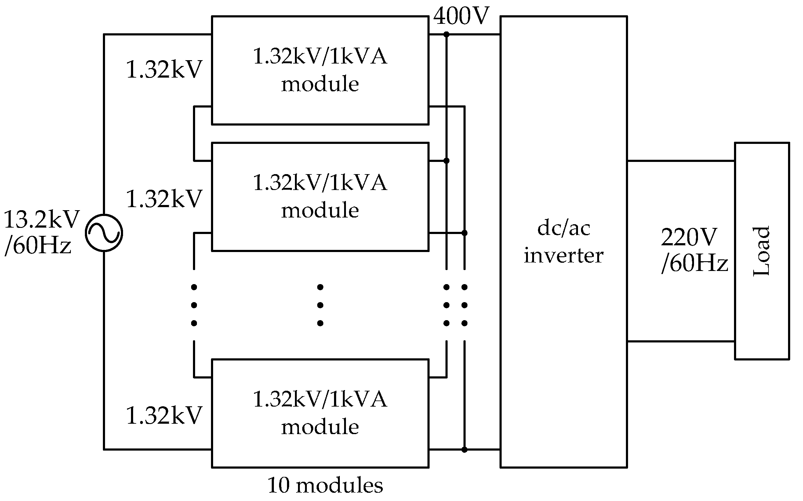
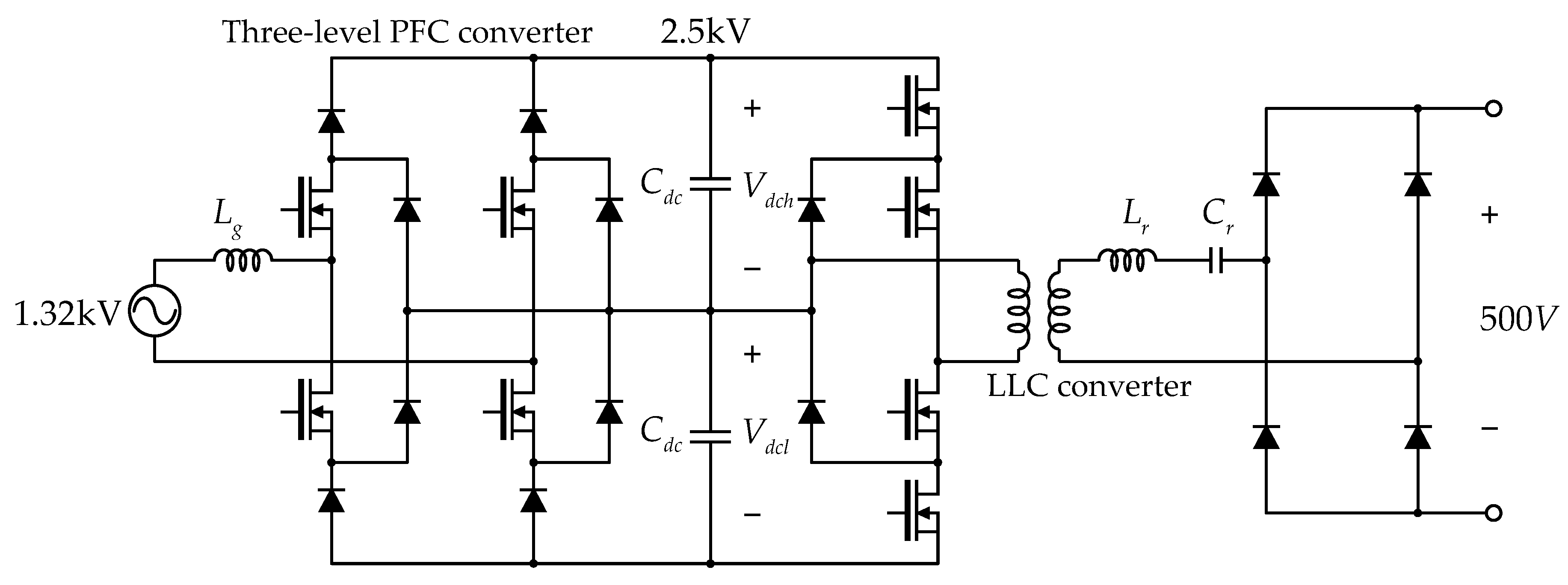
2.1. Power Stage Configuration

Figure 2 illustrates the entire power stage configuration of the SST dealt in this paper. In the Republic of Korea, the primary voltage of the distribution stage is standardized as 13.2 kV in rms. In order to handle such the high voltage, a total of 10 modules are cascaded. The input voltage of each individual module is 1.32 kV, so that 1.7 kV or 3.3 kV switching devices can be employed according to the topology of the circuit. The outputs of the modules are paralleled while generating 500 V in DC. The final purpose of the SST is to supply 220 V/60 Hz load. To do this, a load inverter is connected at the output of the module. Since there are a lot of research articles for such a low voltage standalone inverter, the discussion about the inverter is not addressed in this paper.
Figure 3 illustrates the circuit configuration of the 1.32 kV/1 kVA module. Here, the three-level PFC converter is implemented for PFC operation of the input current as well as establishing the DC-link voltage which is the sum of Vdch and Vdcl. It should be noticed that the three-level PFC converter is a unidirectional converter so that the reverse power flow from the load to the grid is not allowed. Nevertheless, the three-level PFC topology is beneficial in the application, where the unidirectional SST is necessary, because of the efficiency and the simple control. Moreover, the DC-link voltage imbalance is less than other bidirectional three-level topologies such as neutral point clamped (NPC) and T-type NPC structures due to the less number of non-controllable switching states and balanced high frequency (HF) transformer construction [20,26]. At the output of the three-level PFC converter, the LLC converter is connected to produce 500 V DC output from 2.5 kV DC-link voltage as well as guaranteeing an electrical isolation. It should be noticed that the LLC converter is operated in the open-loop control manner to simplify entire control loop of the SST. It will be detailed in a later section.

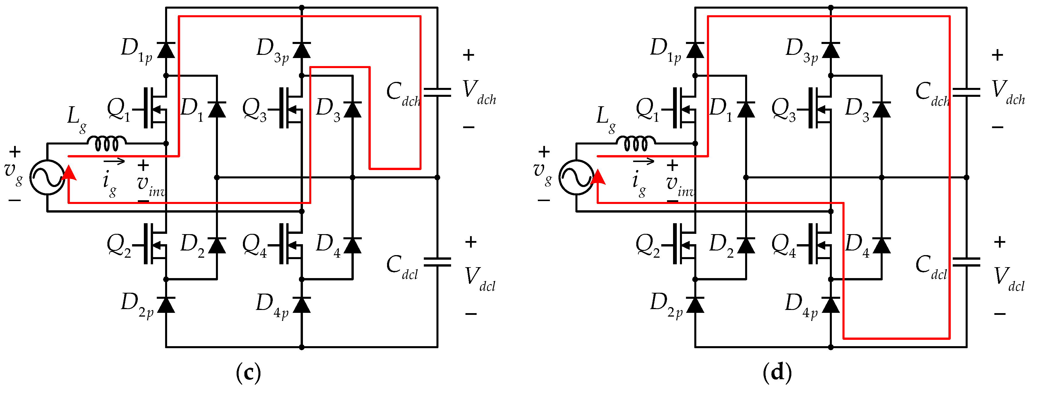
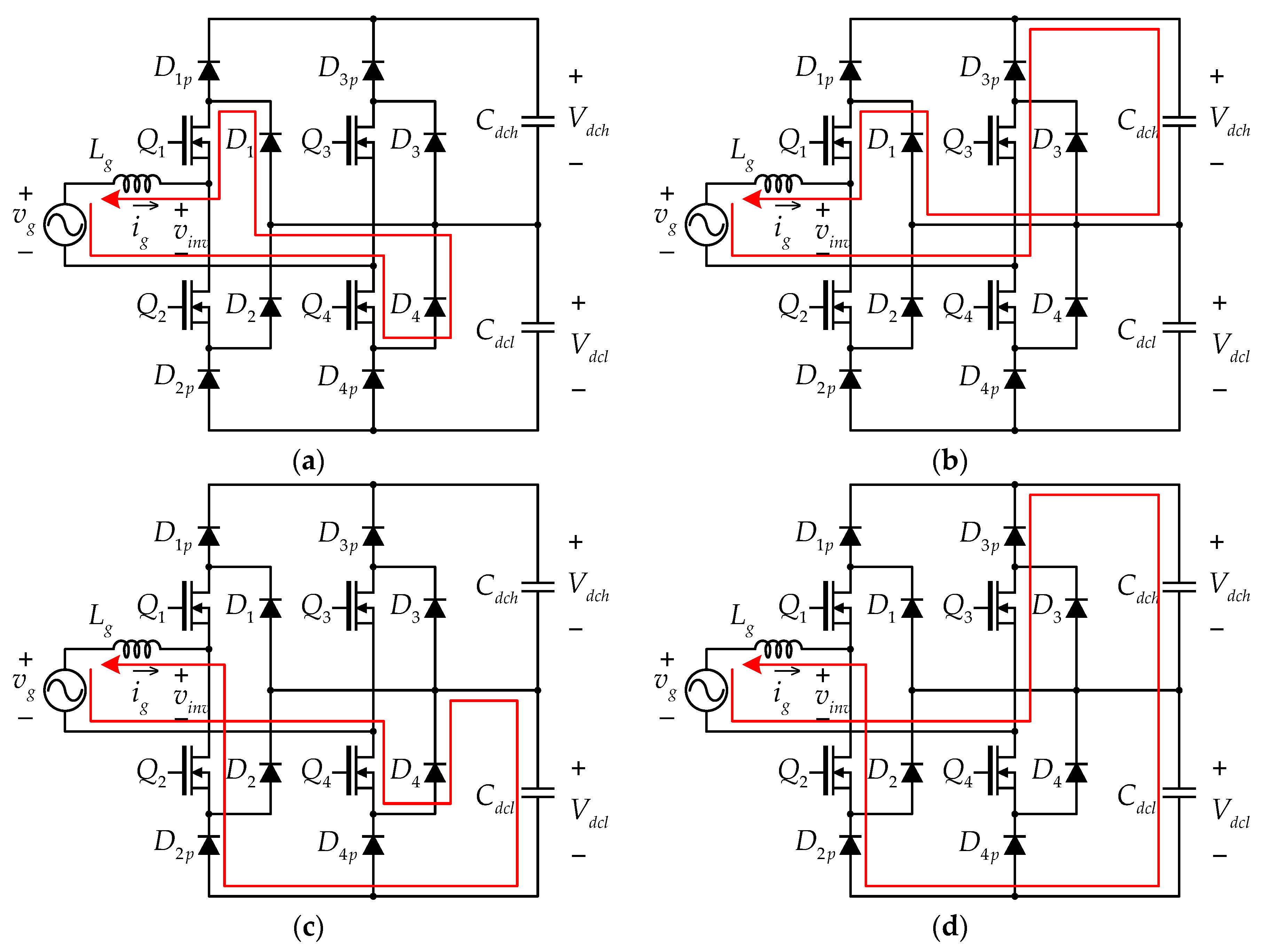
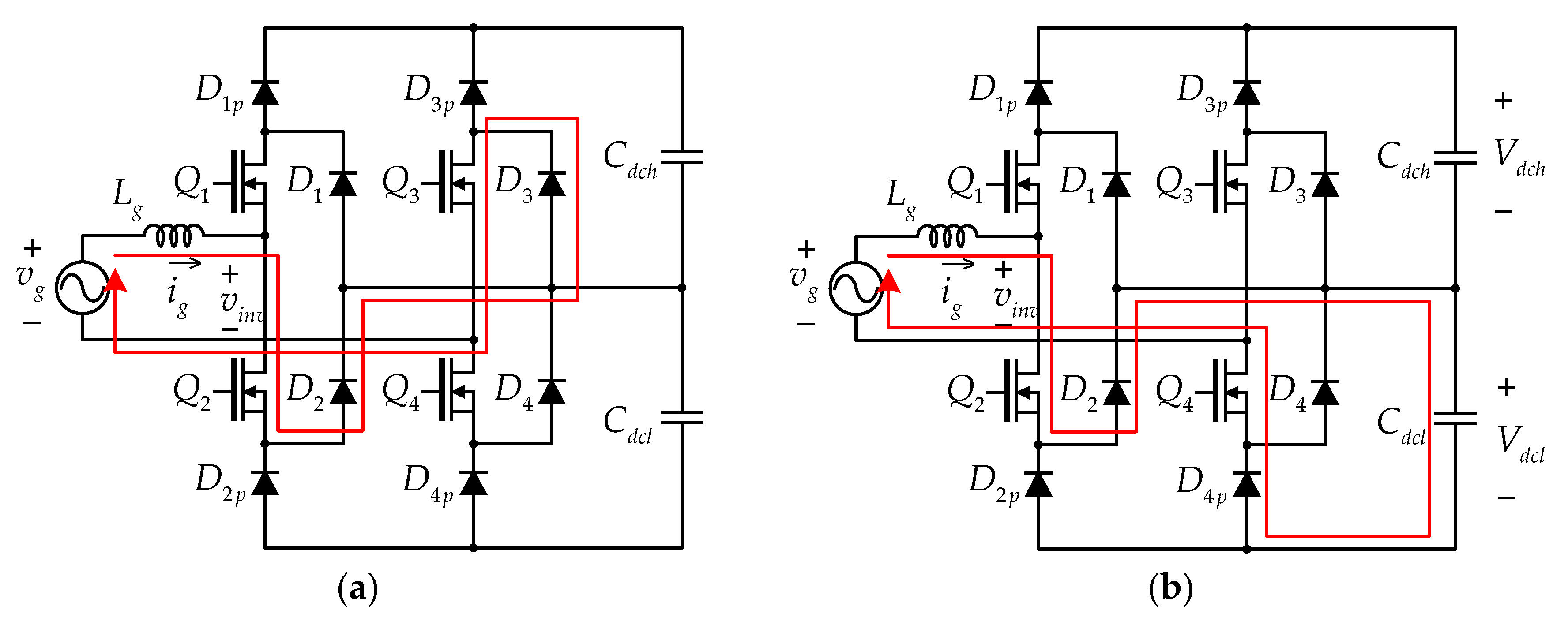
2.2. Three-Level PFC Converter Operation

The operation modes of the three-level PFC converter are determined by the direction of the input current and the status of the switching devices. Figure 4 depicts the current conduction paths of the converter when the input current ig is under positive cycles. Here, four different modes are addressed according to the switching functions which are expressed as the combinations of the switching signals as follows:
Q = ( q 1 , q 2 , q 3 , q 4 )
where q1, q2, q3, and q4 are the elements of the switching function which correspond to the status of Q1, Q2, Q3, and Q4, respectively. Here, the value of an element becomes 1 if the matching switch turns on whereas it becomes 0 when the switch turns off.
Figure 4a shows the current conducting path when all switches are turned on. At this moment, ig flows through Lg, Q2, D2, D3, Q3, and the voltage source, and the energy is stored in the inductor Lg. Even if Q1 and Q3 turn on, no power flows from the DC-link to the grid because of the blocking diodes D1p and D3p. The inductor current ig and the pole voltage of the PFC converter vinv are represented as:
d i g d t = v g L g
v i n v = 0 V
In Figure 4b, Q3 turns off while the others are under turned on. In this case, ig flows through Lg, Q2, D2, Cdcl, D4p, Q4, and the voltage source. The energy stored in Lg is transferred to the lower DC-link capacitor Cdcl. Here, the current flows from the source to the drain in Q4. Since the gate signal of Q4 is applied, the current conducting path in Q4 does not pass the internal body diode, which has poor switching characteristics, but the channel whose conduction and switching losses are relatively lower than the body diode. By doing so, the losses induced in Q4 can be significantly reduced. This is based on exactly the same concept with a synchronous rectification mode of a DC-DC converter using MOSFETs [27,28,29]. The inductor current and the pole voltage are written as:
d i g d t = v g V d c l L g
v i n v = V d c l
Figure 4c illustrates the current conduction path when Q is (1,0,1,1). Again, the stored energy in Lg is transferred to the DC-link, and the upper capacitor Cdch takes it. The current conduction path consists of Lg, Q1, D1p, Cdch, D3, and the voltage source. Similar to the case of Figure 4b, Q1 conducts the current from the source to the drain through the channel. While the pole voltage is the same with (5), the inductor current is obtained as below.
d i g d t = v g V d c h L g
The last case where Q is (1,0,0,1) is shown in Figure 4d. At this instant, the inductor current passes through Lg, Q1, D1p, Cdch, Cdcl, D3p, Q4, and the voltage source as well as discharging the energy stored in Lg. Both Q1 and Q4 are conducted through the channels in reverse. The equations for ig and vinv are represented as follows:
d i g d t = v g ( V d c h + V d c l ) L g
v i n v = V d c h + V d c l
It is interesting that Q1 and Q4 keep turn-on continuously for positive cycles, and only Q2 and Q3 alter their switching status as can be seen in Figure 4. In fact, the modulation strategy using these switching combinations are suitable for reducing a conduction loss in a power stage employing MOSFETs, because the poor internal body diodes in MOSFETs do not turn on [30,31]. However, it may not be a good solution for a power stage using insulated gate bipolar transistors (IGBTs). In such cases, simple modulation methods [30,31,32] can be acceptable.
Similarly, the current conduction paths for ig < 0 are shown in Figure 5. The operational principle is identical to the previous case where ig is positive except the switching combinations and the pole voltage whose values can be 0 V, −Vdch, −Vdcl, and −(Vdch + Vdcl). As compared to the previous case, the status of Q2 and Q3 are not changed while the ones of Q1 and Q4 are continuously changed in every switching cycle.
Table 2 summarizes the relationship between the switching functions and the pole voltages including all cases. If Vdcl and Vdch are well balanced, so that their magnitudes are the same as Vdc, the PFC converter has five levels in total: −2Vdc, −Vdc, 0 V, Vdc, and 2Vdc. It is well-known that carrier-based modulation strategies are simple, and much research has been conducted for the carrier-based pulse-width-modulation strategies in NPC applications [33,34,35]. Hence, a simple carrier-based method is employed in this paper.
Figure 6a describes the modulator structure of the PFC converter to achieve the current conduction modes addressed in Figure 4 and Figure 5. The limiter 1 only extracts the positive component from the original duty reference while the limiter 2 obtains the negative one. Let us assume that the grid current ig is well regulated with unity power factor operation. When ig is positive, Q1 should be always turned on, and Q2 is switching according to d2. If ig is negative, the roles of Q1 and Q2 are exchanged. For the switching leg consisting of Q3 and Q4, the inverse of the original duty reference is applied. By doing so, the effective switching frequency becomes double, and the switching ripple on the inductor current is significantly reduced.
Although the structure shown in Figure 6a is completely suitable for the power stage in this paper, it requires four different carrier signals. This may be a significant burden for the digital controller, and the implementation will be complicated. To simplify the realization, the modified structure for the modulator is proposed in Figure 6b. In the modified structure, only two carrier signals (whose phase difference is 180 degrees) are necessary, and the method to extract individual duty references d1, d2, d3, and d4 is slightly different. By doing so, the process shown in Figure 6b is exactly equivalent to the structure illustrated in Figure 6a.

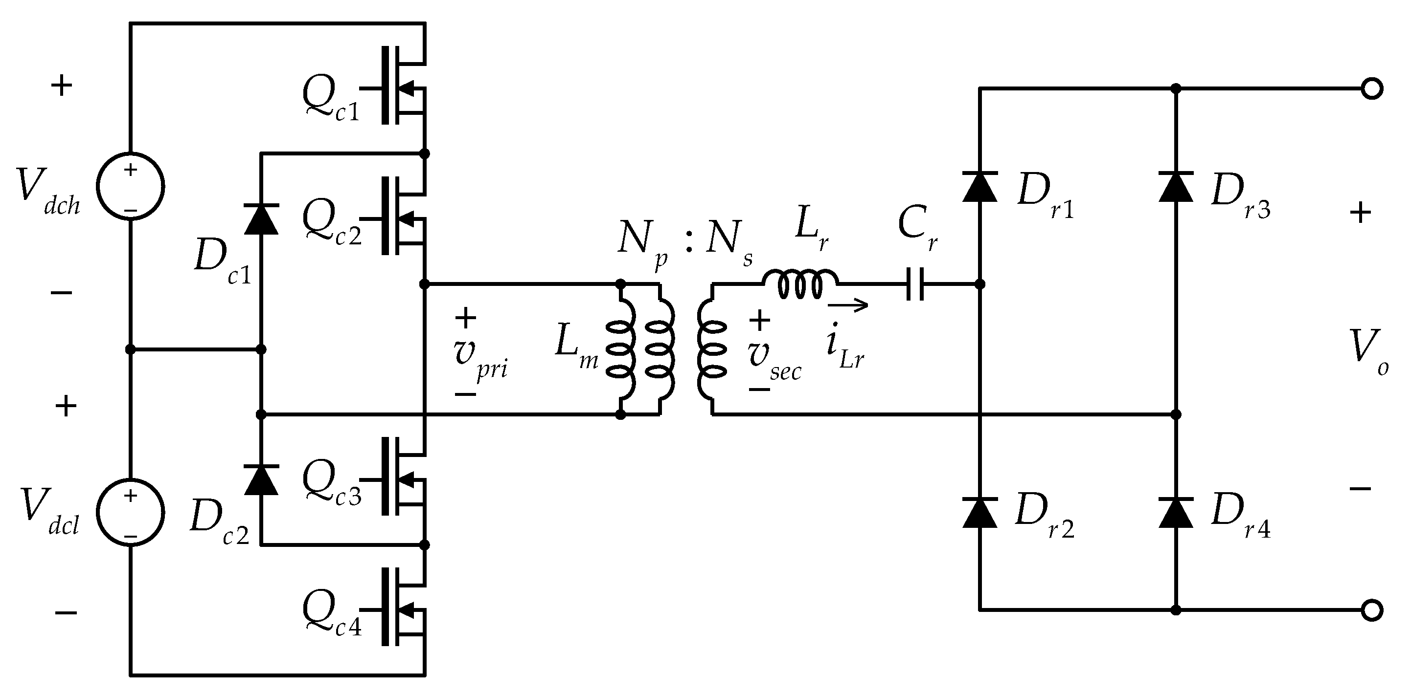
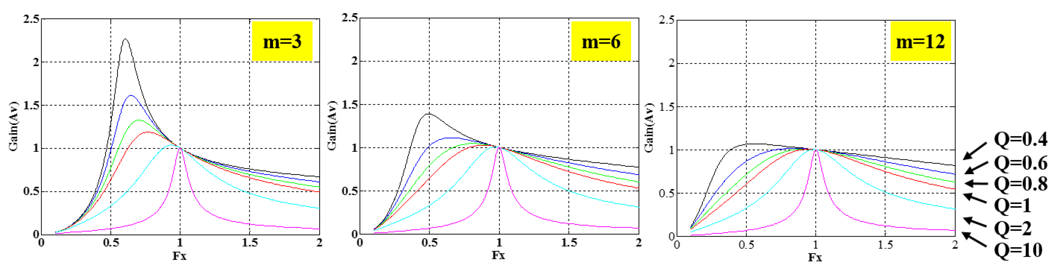
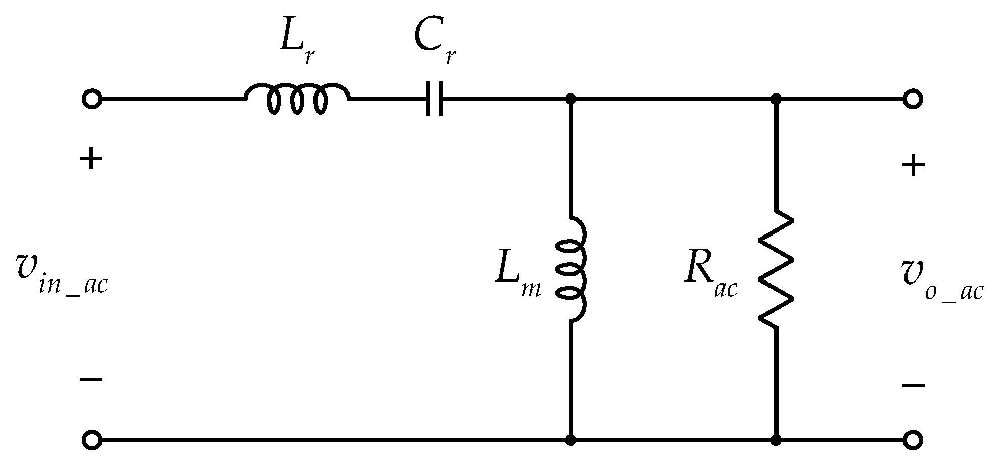
2.3. LLC Converter Operation

Figure 7 depicts the circuit configuration of the LLC converter. It is fed by the separate DC sources Vdch and Vdcl which are established by the output of the front-end PFC converter. The main switching circuit is implemented in the manner of NPC type inverter, but the switching scheme is different. In the LLC converter, the upper and the lower switch pairs are defined. The upper switch pair consists of Qc1 and Qc2 while the lower switch pair contains Qc3 and Qc4. Unlike NPC inverters, each switch pair operates as a single switch, so that the switch elements in a switch pair alter their status simultaneously. As a result, the output voltage vpri reveals a two-level voltage whose peak and valley values are Vdch and Vdcl. Meanwhile, the rating of individual switching devices can be cut by half due to the clamping action of DC1 and DC2. At the output of the NPC inverter, the isolated HF transformer and the LC resonant tank are existent. Since the output of the resonant tank is AC voltage, the diode rectifier composed by Dr1, Dr2, Dr3 and Dr4 is necessary. In order to design the LLC converter, let us consider the equivalent resonant circuit as shown in Figure 8 where Lm, Lr and Cr are the magnetizing inductance of the HF transformer, the resonant inductor, and the resonant capacitor, respectively [36].
The resonant tank gain is defined as follows:
K = | V o _ a c ( s ) V i n _ a c ( s ) | = F x 2 ( m 1 ) ( m F x 2 1 ) 2 + F x 2 ( F x 2 1 ) 2 ( m 1 ) 2 Q 2
where Vo_ac(s), Vin_ac(s), Q, m, and Fx are the Laplace transformations of vin_ac and vo_ac, the quality factor, the ratio of the total primary inductance to resonant inductance, and the normalized switching frequency. They are represented as:
Q = L r C r R a c
m = L r + L m L r
F x = f s f r
Here, fs is the switching frequency, and the resonant frequency fr and the reflected load resistance Rac are written as:
f r = 1 2 π L r C r
R a c = 8 π 2 N p 2 N s 2 R o
where Np, Ns, and Ro are the primary turns ratio, the secondary turns ratio, and the load resistance.
Figure 9 compares the voltage gains under different m and Q factors. In the figure, the voltage conversion ratio can be extended as decreasing m factor. However, a low m factor requires a low Lm, so that the magnetizing current increases. Thus, the conduction loss of the magnetic component is increased. In terms of Q factor, it is proportional to the load. According to the figure, the voltage gain cannot be higher with a heavy load. In fact, the voltage gain is changed by both m and Q factors.
One simple approach to select these parameters is setting the switching frequency to be the resonant frequency, so that Fx becomes 1 [36,37,38]. By doing so, (9) can be simplified as below.
K = | v o _ a c v i n _ a c | = ( m 1 ) ( m 1 ) 2 = 1
It means the voltage gain of the resonant tank is the unity. Hence, the output voltage is determined by the primary and the secondary turn ratio of the HF transformer. By this way, the LLC converter can be considered as a DC transformer.

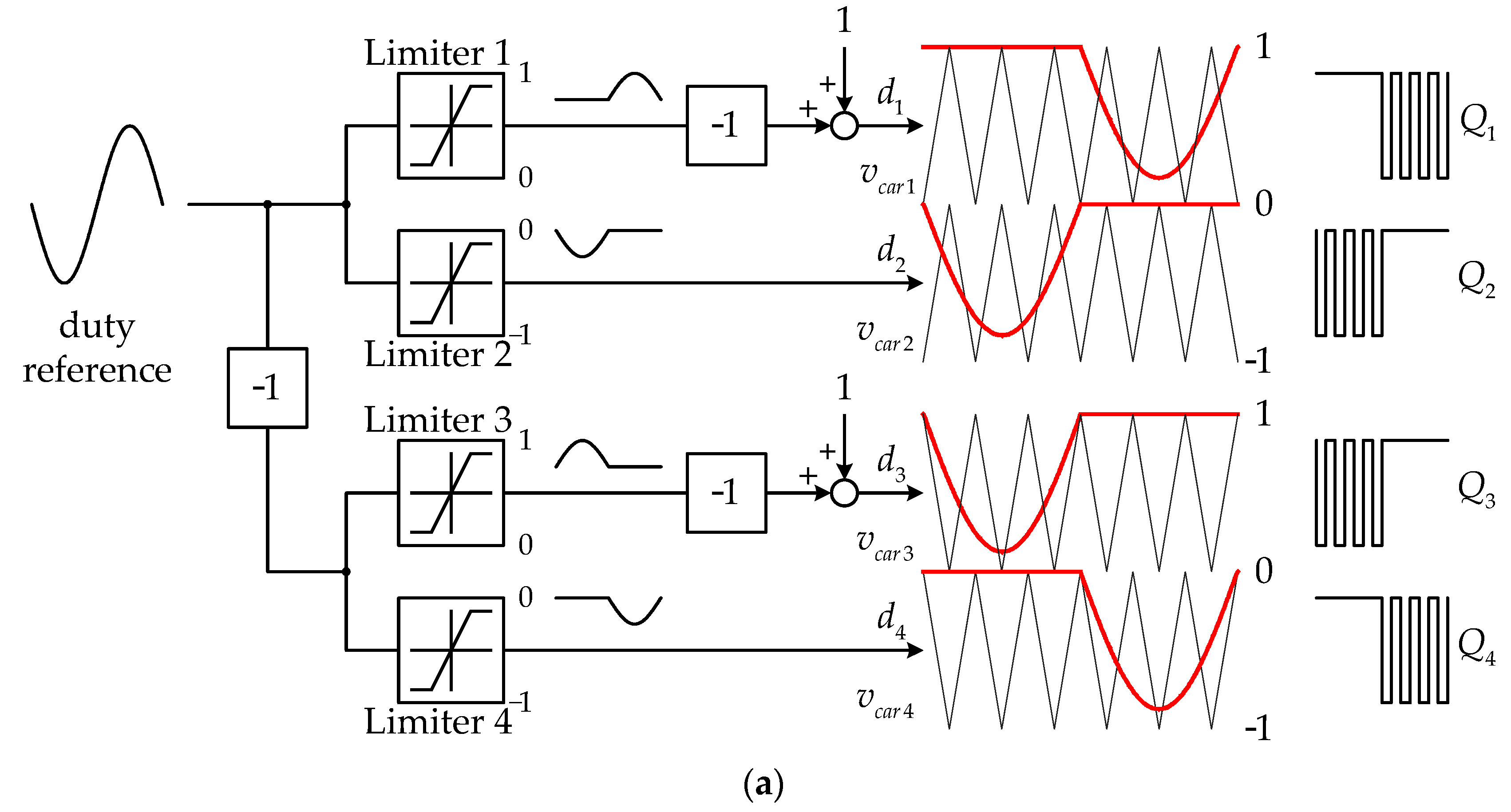
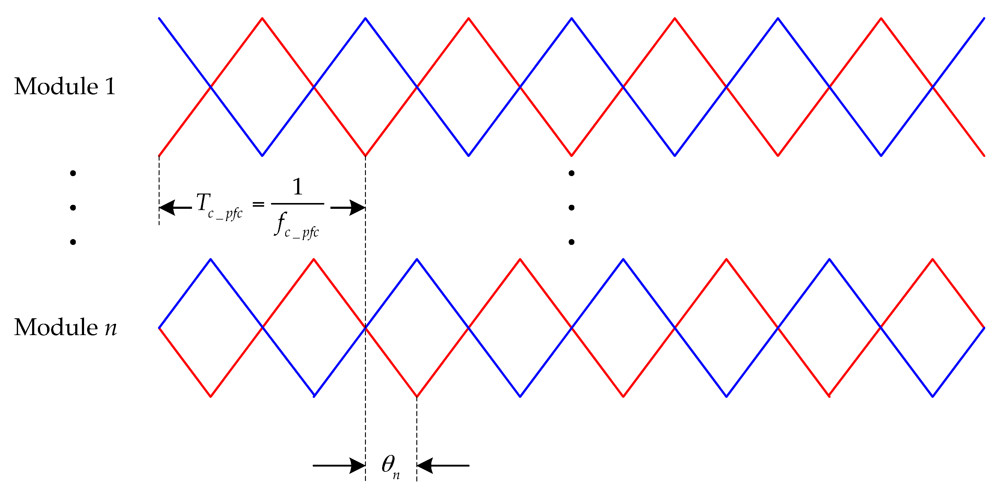
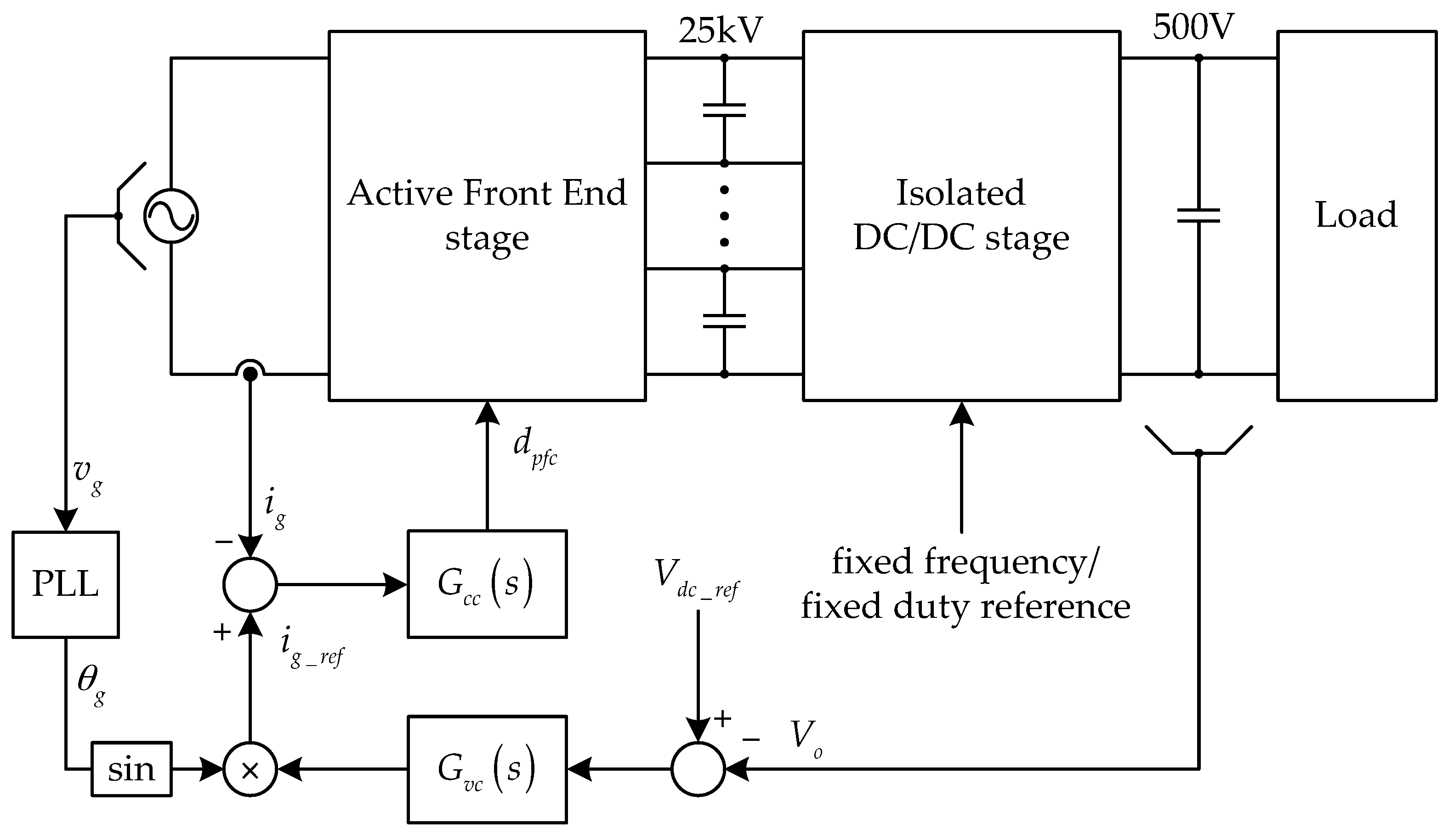
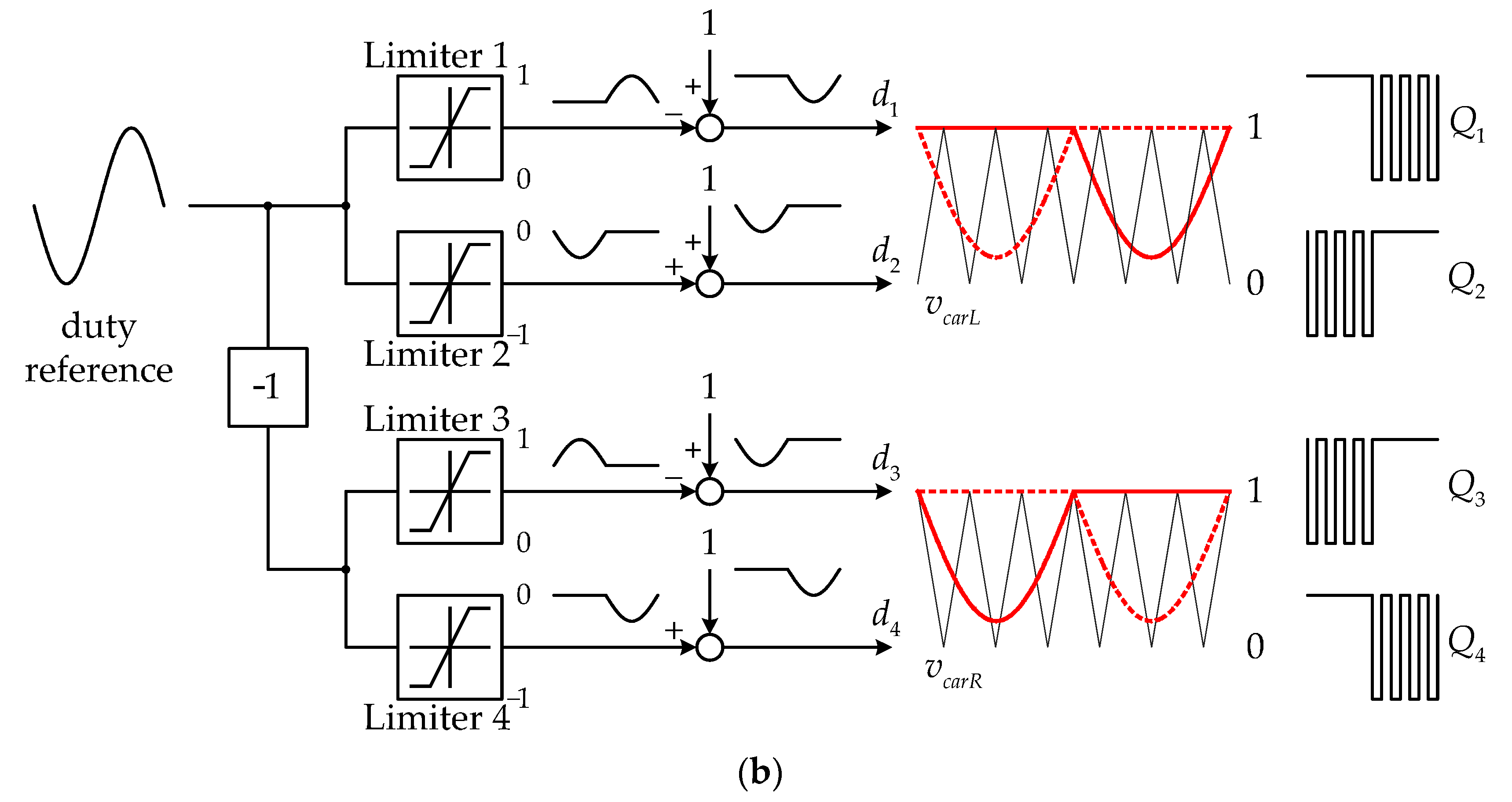
2.4. Control Strategy of the Power Stages

In a single module, the switching frequency of the three-level PFC converter is effectively double the original one, because the interleaved operation is achieved by employing the two carriers with 180 degrees of phase difference. In the whole active front end stage, where a total of 10 modules are connected, the three-level PFC converters in the stage are cascaded to distribute such the high input AC voltage into the individual modules. In addition, the phase shift modulation is applied for the entire cascaded PFC converters.
Figure 10 depicts the carrier waveforms for individual modules. Let us assume that the number of the modules is represented as N. From the figure, the phase difference θn between nth module and the first module is represented as [39,40,41]:
θ n = 180 N ( n 1 ) degree
The effective switching frequency fsw_pfc considering the phase difference is written as:
f s w _ p f c = 2 N × f c _ p f c
where fc_pfc is the carrier frequency of a switching leg. As can be seen in (17), the effective switching frequency can be increased as proportional to N. Figure 11 shows the entire control structure of the SST. For the isolated DC-DC stage, the switching signals are modulated with a fixed frequency with a fixed duty reference, so that technically no closed-loop control is applied to the stage. The isolated DC-DC stage only interfaces between the high voltage primary and the low voltage secondary sides. Once the turn ratio of the HF transformers in the isolated DC-DC stage is determined, the secondary output voltage Vo is directly proportional to the primary DC-link voltage. It means the regulation of Vo is achieved by adjusting the primary DC-link voltage. However, it is not that simple, because the primary DC-link voltage of the isolated DC-DC stage consists of cascaded multiple DC-links. It requires 10 DC-link voltage sensors. In addition, the signal conditioning circuitries to interface the individual DC-link voltage sensor require at least 20 kV of isolation capability. Apparently, these increase the implementation cost and complexity. In order to resolve this issue, the voltage controller Gvc(s) directly regulates Vo by controlling the input current of the AFE stage. The controller consists of the voltage controller Gvc(s) and the current controller Gcc(s). For the voltage and the current controllers, a proportional-integral (PI) and a proportional-resonant (PR) structures are employed. The output of Gvc(s) is multiplied by the phase angle detected from the phase-locked-loop (PLL), and the input current reference ig_ref is obtained. After that, ig is regulated to track ig_ref by the operation of Gcc(s). The output of Gcc(s) is dpfc which is the duty reference of the AFE stage. The PFC modules in the AFE stage shares dpfc, but the phases of individual PFC modules are different by reflecting (16).

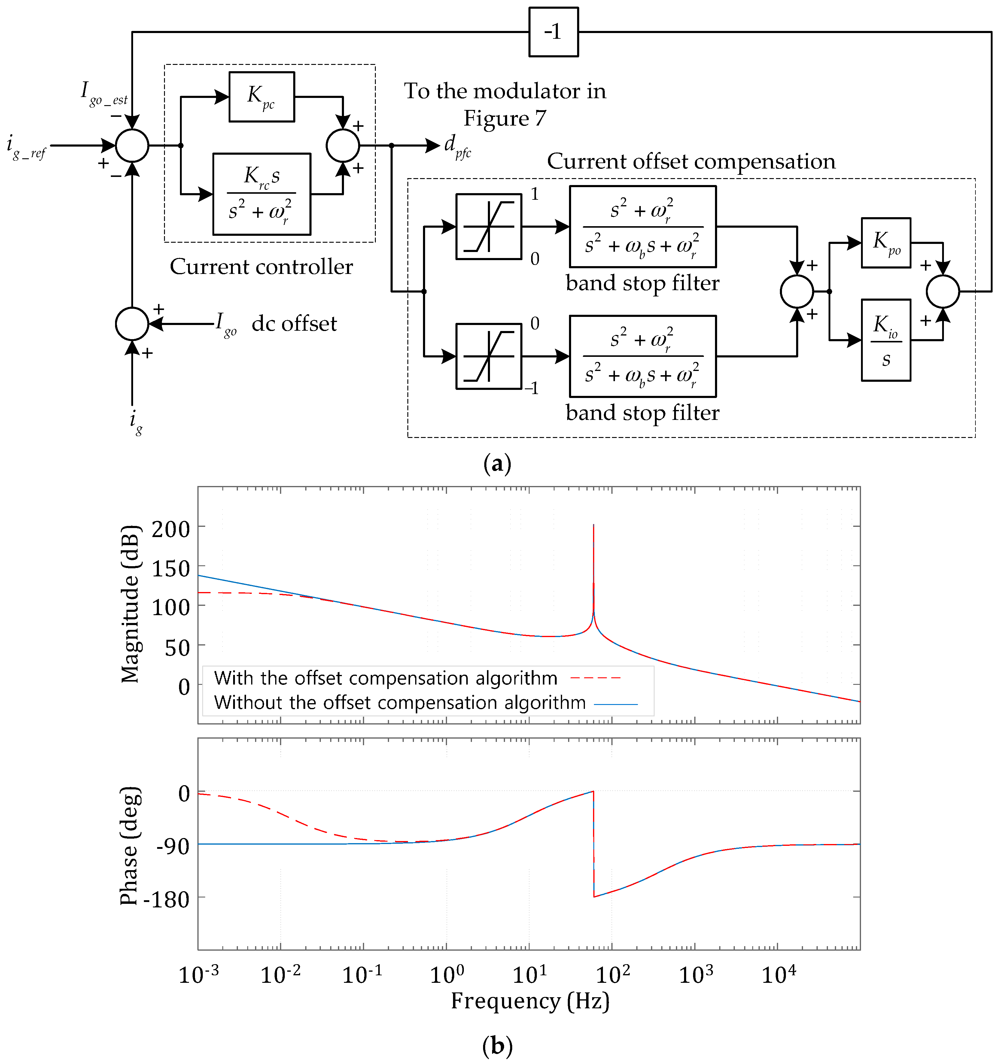
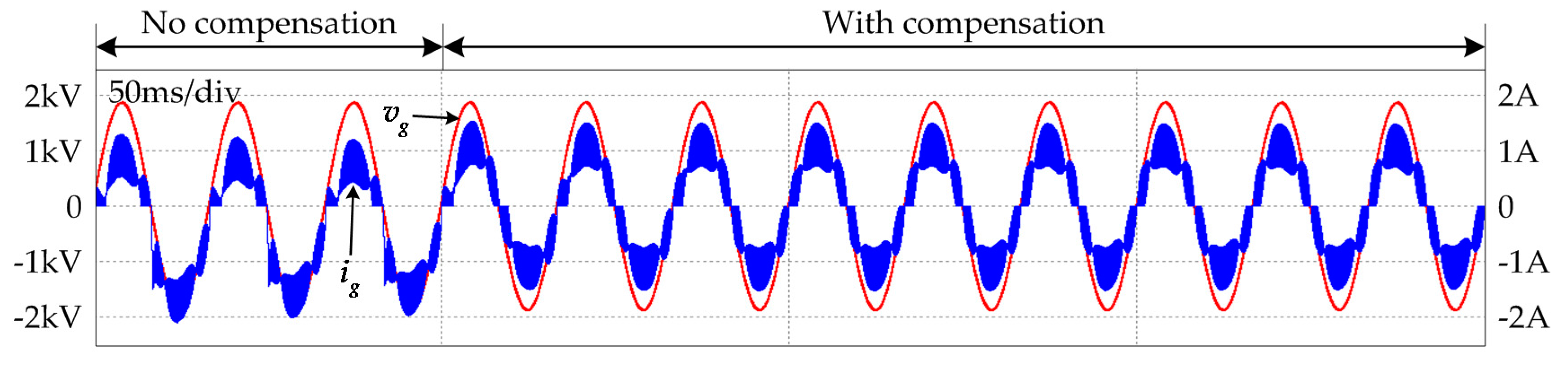
3. Proposed Input Current Offset Compensation Method

For a grid-tied power electronic converter, the input AC current should not contain any DC offset component to prevent a DC excitation to the power grid and the distribution transformer, where the converter is connected. However, it is hard to avoid a measurement offset on the current sensor used in a converter. In order to mitigate the problem, an offset compensation algorithm is proposed. Figure 12a shows the proposed offset compensation method including the PR current controller. Assume that there is the DC offset Igo in the current measurement path. Then, the error, which is the input of the PR controller, is represented as:
i e r r = i g _ r e f i g I g o
Here, the estimated DC offset Igo_est is not contained. Then, the output of the PR controller only considering Igo is written as:
i e r r _ g o = I g o ( K p c + K r c s s 2 + ω r 2 )
where ωr is the fundamental frequency of the grid. Since Igo can be considered as a unit step function with the gain Igo, the inverse Laplace transform of (19) is obtained as (20).
I e r r _ g o = K p c I g o + K r c I g o sin ( t ω r ) ω r
In fact (20) is a part of the duty reference dpfc, and the first term of the right-hand-side (RHS) is apparently a DC component. From this, it is supposed that a DC offset induces a DC component in dpfc which is the output of the PR controller.
Here, dpfc is taken as the input of the current offset compensation block, which consists of the limiters, the band stop filters (whose cut-off frequency is ωr), and the proportional-integral (PI) estimator. In the compensation block, the positive and the negative parts of dpfc are distinguished by the limiters. After that the band stop filters are applied the DC component KpcIgo in dpfc is extracted. If Igo is a positive value, the upper branch in the current offset compensation block has a positive output while the lower block shows zero value. On the other hand, the lower block has a positive value with a negative Igo. The output of the PI estimator Igo_est, which is the estimated DC offset, is connected to the current feedback junction and is adjusted to obtain zero at the input of the estimator. As long as the input of the estimator is zero, it is supposed that there is no DC component in dpfc. It means there is no DC offset in the current measurement path. Figure 12b analyzes the open-loop gain of the proposed control loop including the offset compensation algorithm. The duty reference to the inductor current model Gid(s) is simply assumed as a first model shown in (21).
G i d ( s ) = V d c h + V d c l L g s
Without the offset compensation algorithm, the loop-gain in Figure 12b shows a typical open-loop frequency response of an inductor current model adapting a PR controller whose proportional and resonant gains are 0.2 and 500, respectively. The magnitude at the fundamental frequency 60 Hz is evaluated as 200 dB. The phase margin is close to 90 degrees. For the offset compensation algorithm, the controller parameters are selected as ωb = 62.83 rad/s, Kpo = 1 × 10⁻⁵, and Kio = 0.2, respectively. As can be seen in the figure, the DC gain is slightly reduced with the offset compensation algorithm. However, it does not affect the entire control performance, because the operating frequency of the control system starts from 60 Hz.

4. Simulation Results

The simulation model of the module shown in Figure 3 is built in Power SIM 9.0 from Power SIM Corporation to examine the power conversion performance. Table 3 gives the parameters used for the simulation study. Figure 13a shows vg, vinv, and ig. At the beginning, the module is operated at the no-load condition. After that, the full load is instantly applied, and the input current ig increases. As analyzed in Table 1, vinv has total 5 levels. Apparently, the unity PF operation is achieved. Figure 13b shows the plot of the secondary side voltage and the current of the HF transformer, vsec and iLr. Due to the resonant tank consists of Lr and Cr, the shape of the secondary side current is sinusoidal.
Figure 14 shows the switching waveforms of the MOSFETs in the LLC converter. In the figure, vds_Qc1, vds_Qc2, vds_Qc3, and vds_Qc4 represents the drain to source voltages of the switching devices Qc1, Qc2, Qc3, and Qc4, respectively. As can be illustrated in the figure, the device currents iQc1, iQc2, iQc3, and iQc4 rise after the devices are fully turned on, so that the drain to source voltages are zero. It means zero-voltage-switching (ZVS) is achieved in the individual devices. A merit of LLC converters is high efficiency, which is expected due to the ZVS guaranteed in these devices.
Figure 15 represents the performance of the proposed offset compensation method. Initially, −0.5 A of current sensing offset is assumed with no compensation. After 3 cycles, the proposed method is applied, and the current offset is eliminated in 4 cycles.
Since 10 modules are employed in the SST, the simulation with total modules working together has been performed. Figure 16 shows vinv and ig at the rated power condition 10 kVA. The input voltage is 13.2 kV in rms. With 10 modules, the input voltage has multiple steps due to the interleaved operation among individual modules, so that the input current ripple is significantly reduced. Theoretically, vinv can have 39 steps with the maximum duty cycle. However, it has 31 steps in the simulation, because the duty cycle does not reach the maximum value.

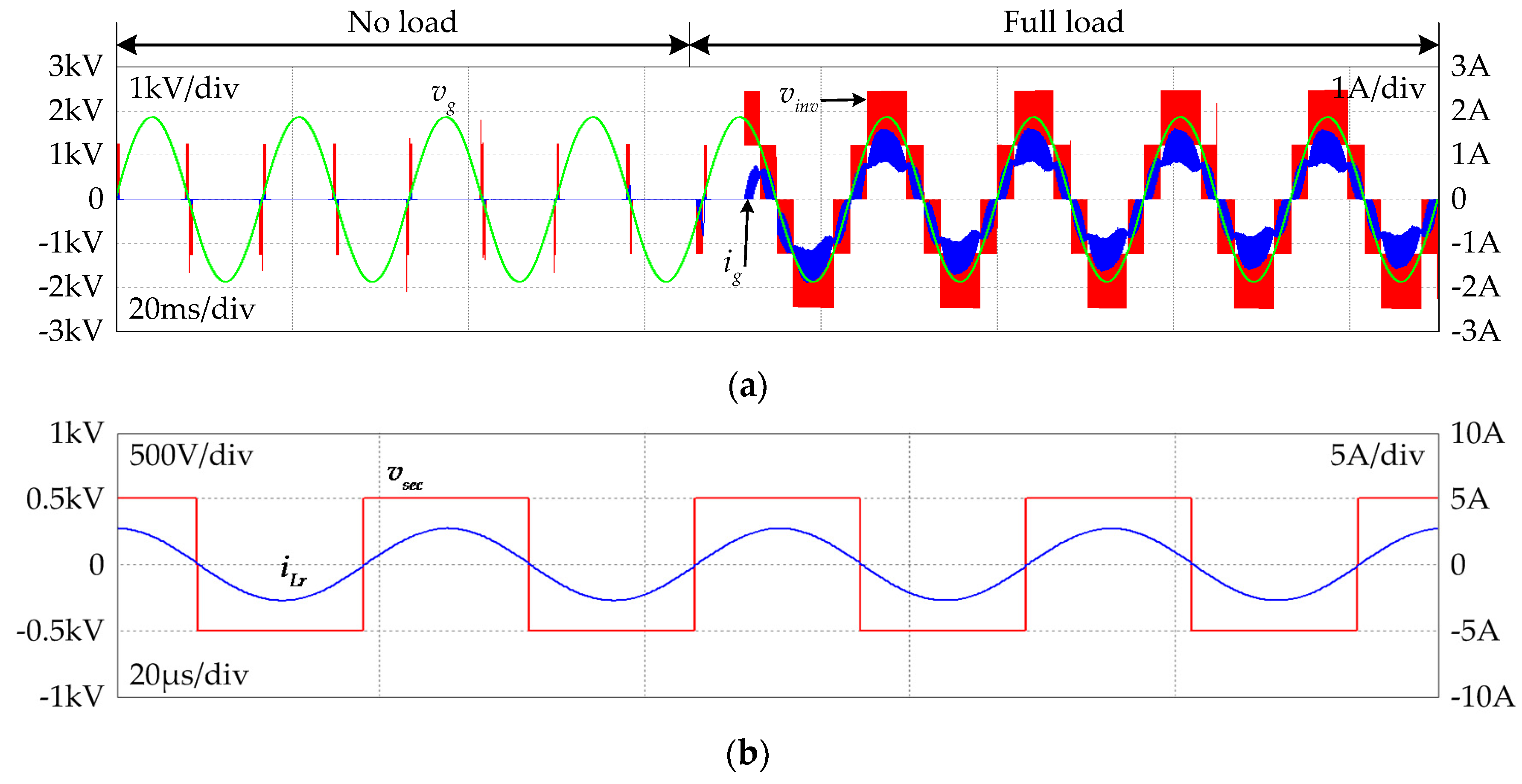
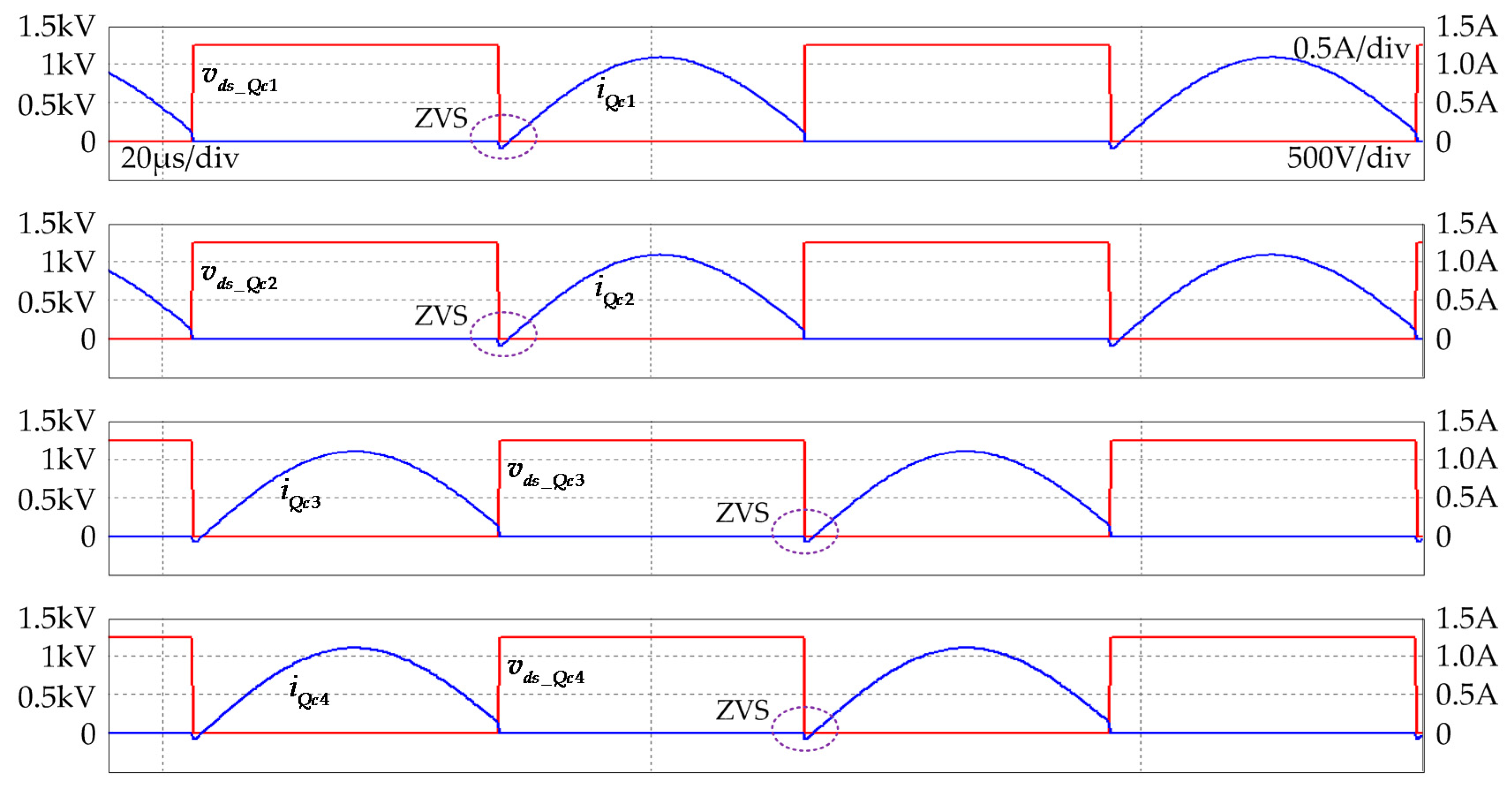
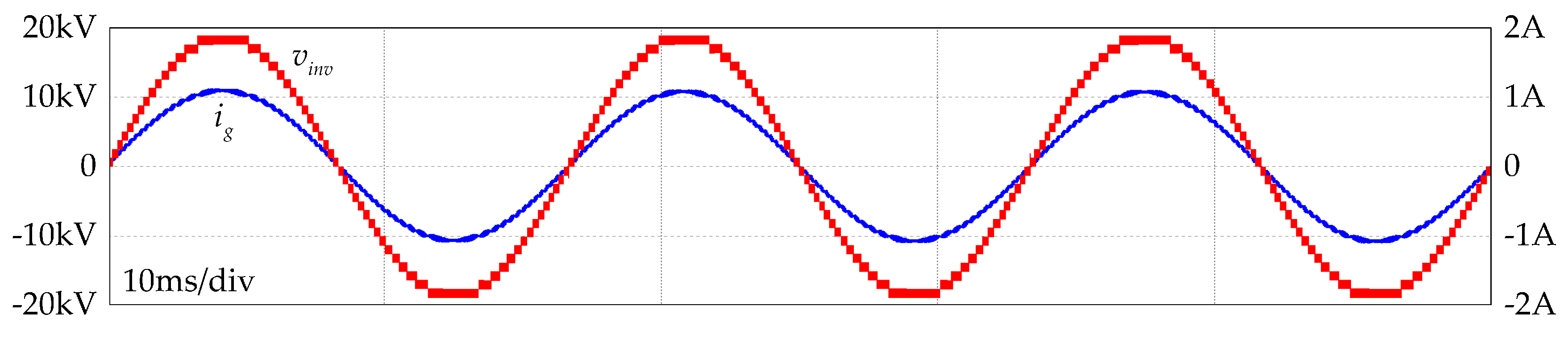
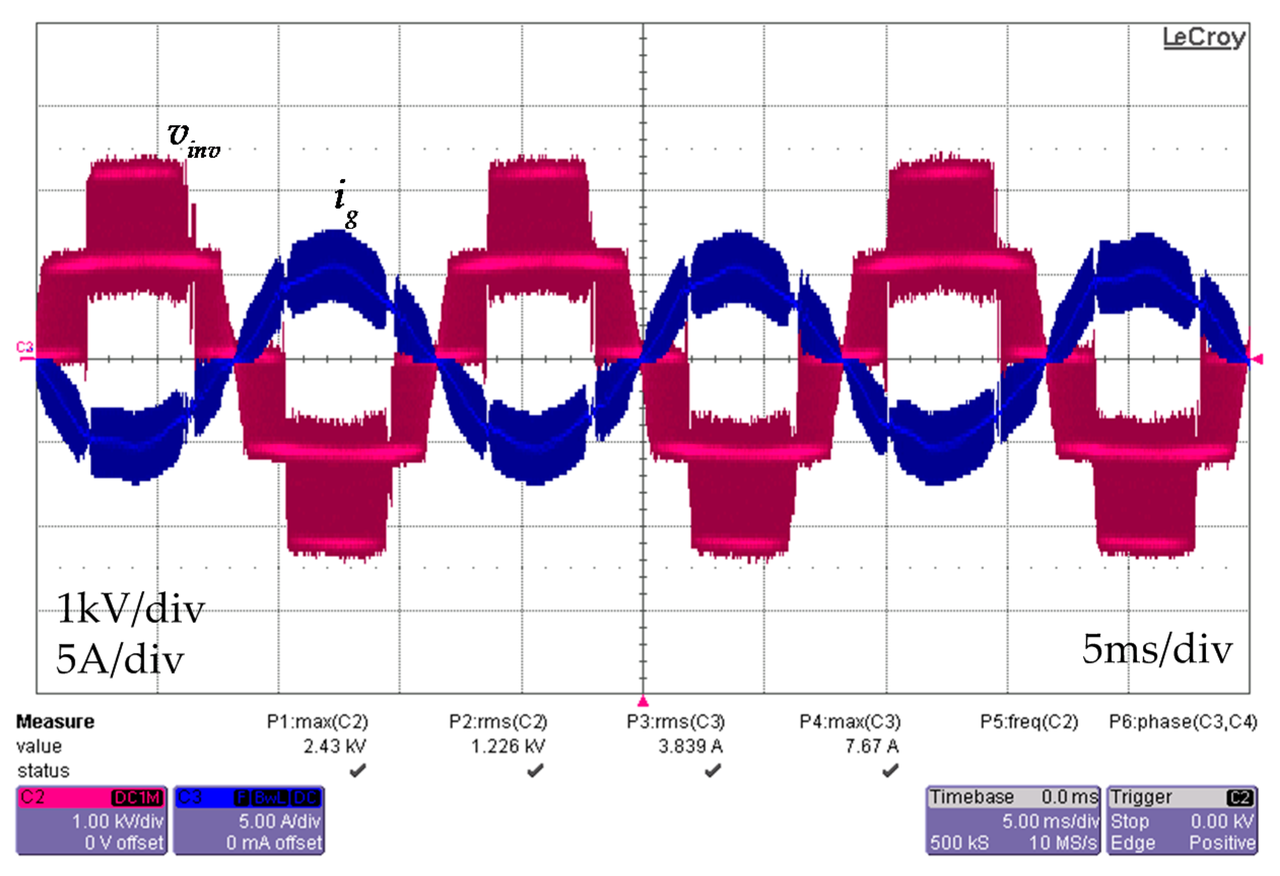
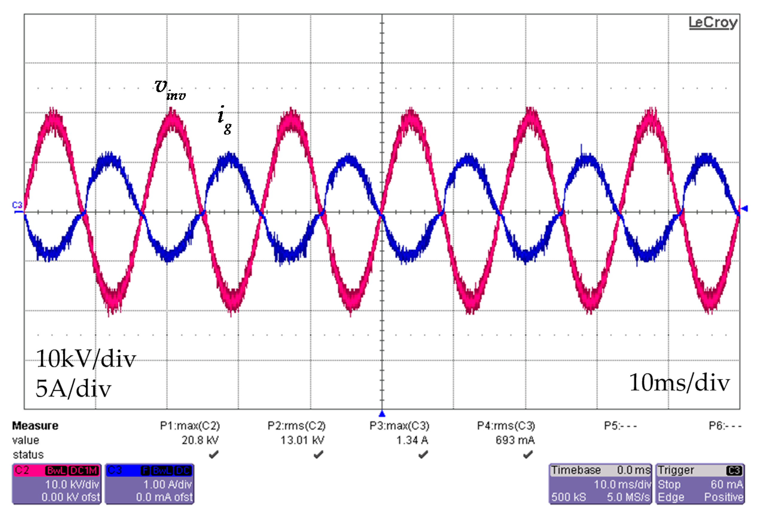
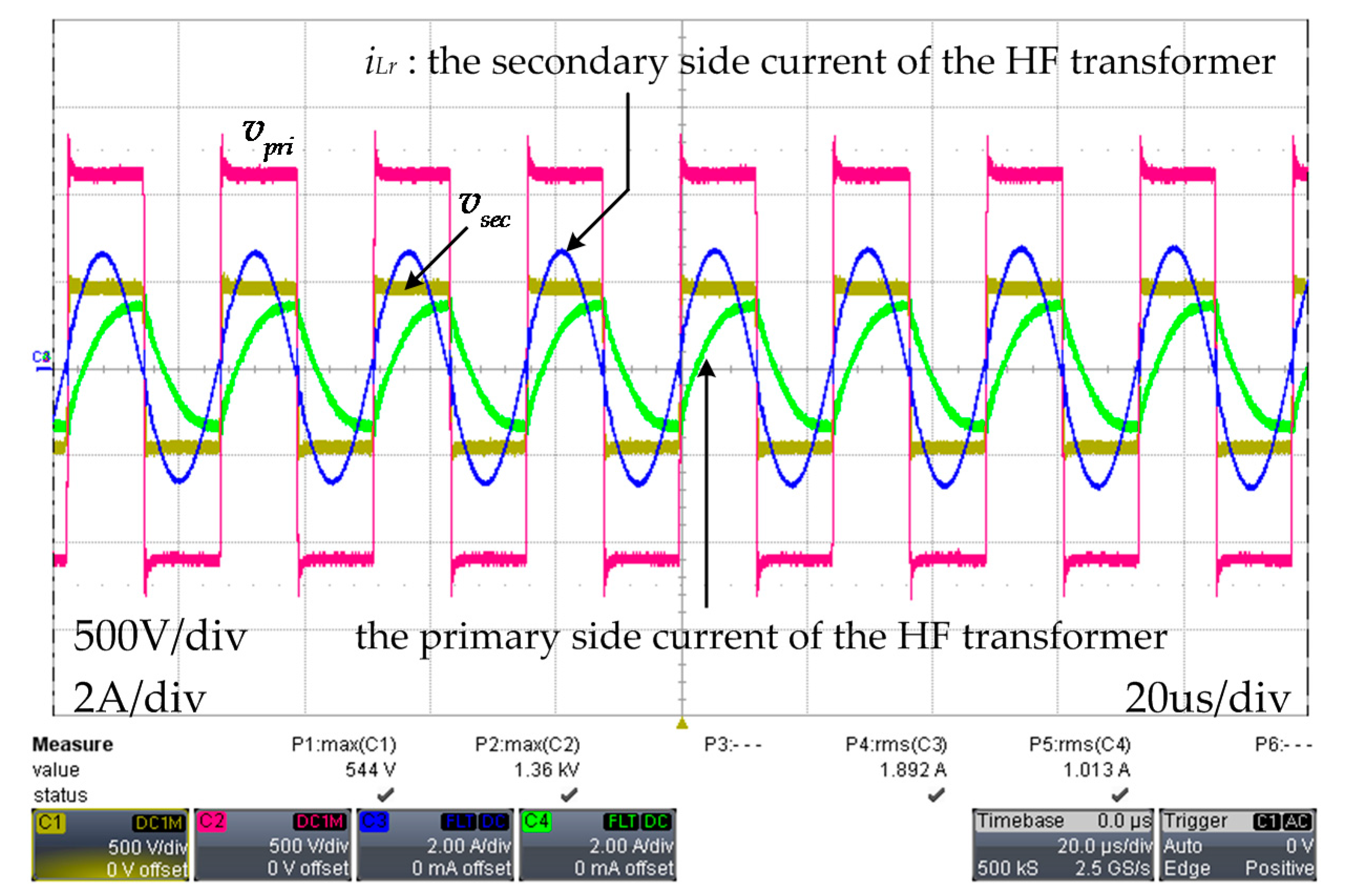
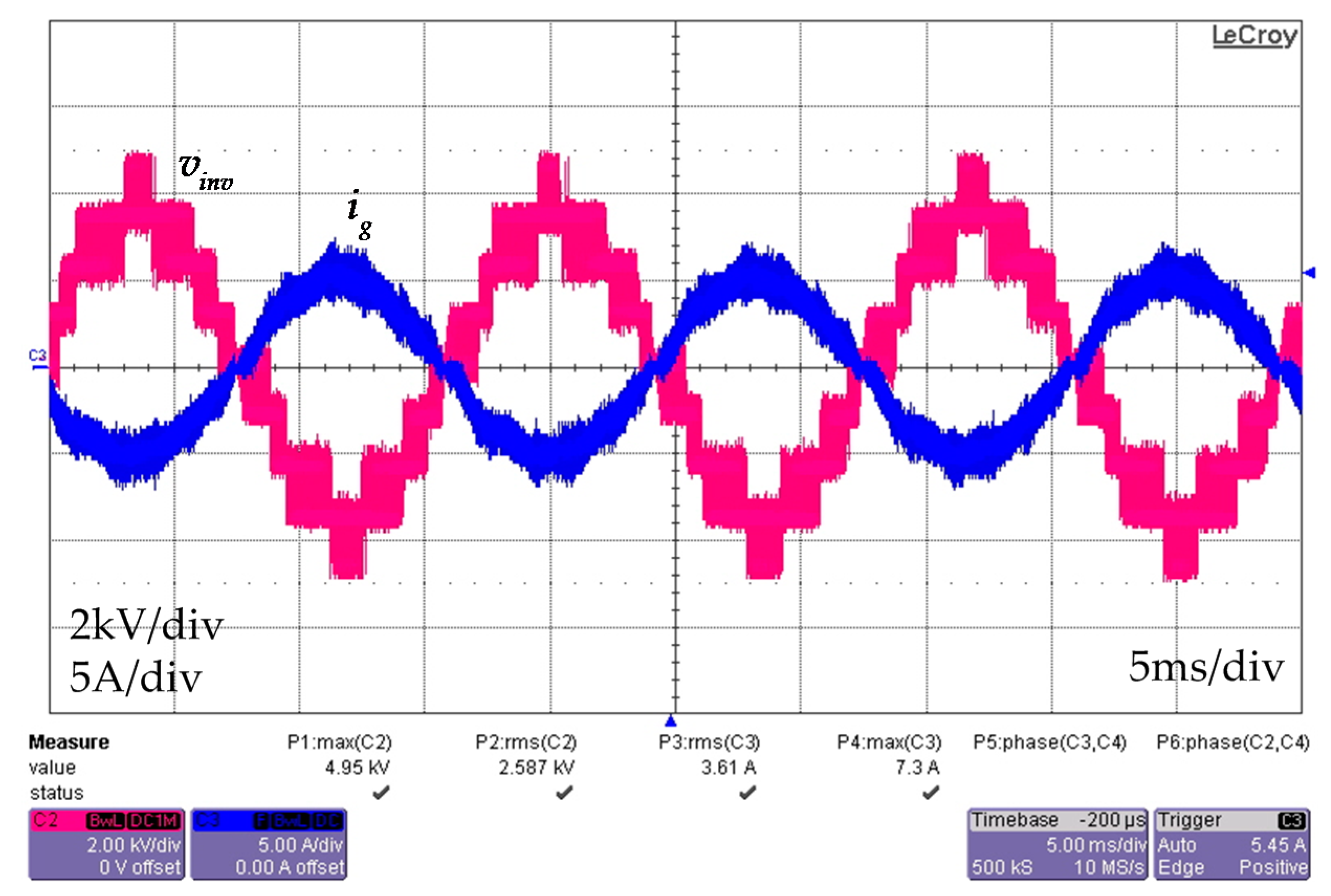
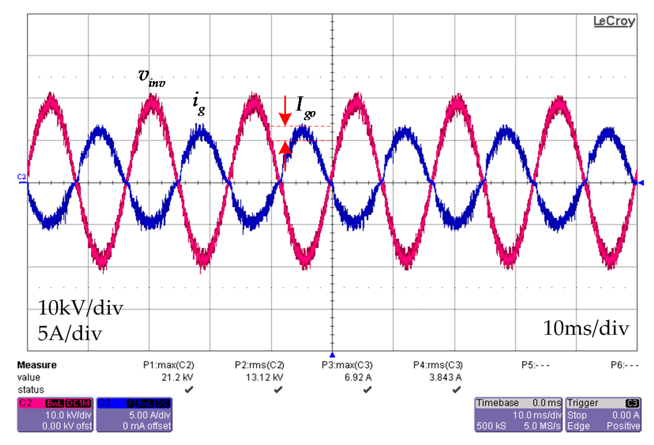
5. Experimental Results

Figure 17 shows a photograph of the experimental setup for the SST prototype. For the load, a resistor load bank is connected to the output of the power stage. The same parameters represented in Table 3 are utilized. To obtain 13.2 kV AC voltage in the laboratory, two transformers, the variac and the pole transformer, are employed. Since the pole transformer is connected to the output of the variac, variable high voltage can be easily obtained to test the SST prototype. In order to measure the high input voltage, a commercial potential transformer is used. For the AFE and the DC-DC converters, Cree’s C2M1000170D MOSFETs and Global Power’s GP2D005A170B devices have been utilized. They are both silicon carbide devices, and the switching frequency can be much higher than using traditional silicon devices. By doing so, the physical sizes of the magnetic components can be significantly reduced. Furthermore, a low switching loss is expected. The control structure of the SST contains a global and a local controller. The voltage and current control algorithms are implemented in the global controller using an in-house developed digital control board based on Texas Instruments’ TMS320F28335. Since the number of the pulse-width-modulation channel in the digital controller is not enough to cover the SST system, which requires 80 channels, the local controllers using TMS320F28035 are equipped in the individual 1.32 kV/1 kVA modules. The local controllers receive the duty reference from the global controller, and they generate interleaved modulation signals. The communication between the global and the local controllers is realized through the optic connected serial peripheral interface buses. The SST was tested at the full load condition, 10 kVA.
Figure 18 demonstrates the switching voltage and the input current of the single AFE converter where the input voltage is 1.32 kV. As analyzed in the previous section, the switching voltage of the AFE converter has five steps. The input current has a significant current ripple, but the power factor is close to the unity. The switching voltage and the input current of the AFE stage with two cascaded modules are shown in Figure 19. The input voltage is 2.6 kV at this condition. Due to the interleaved operation of the two modules, the input current ripple is considerably reduced. Through Figure 18 and Figure 19, it can be recognized that the simulation results performed in the earlier section are well matched with the experimental results.
Figure 20 shows vinv and ig when total 10 modules are operated under 13.2 kV input voltage. Since vinv has multiple steps, which was confirmed in the simulation, its shape is close to sinusoidal. Compared to the previous results, the ripple in the input current is considerably mitigated. Note that the input current offset Igo is existent in the result due to the current measurement offset caused by the non-ideal characteristics of the signal conditioning circuit. In Figure 21, the proposed offset compensation algorithm is applied, so that the current offset Igo is eliminated.
Figure 22 shows the switching voltages and currents of the primary and the secondary sides of the HF transformer in the LLC resonant converter under 10 kVA operation. Since total 10 modules are employed, the output power of the LLC resonant converter is only 1 kW. From the figure, it is supposed that the soft-switching operation has occurred.
Figure 23 shows the thermal simulation of the power stage under 30 percent load with 2 h operating condition. In order to perform the thermal analysis, ANSYS R16.2 academic version is utilized. The ambient temperature is given as 20 degrees Celsius, and a natural cooling is assumed. The maximum temperature is measured as 36.8 degrees Celsius on the diodes. Although it is hard to sense the efficiency accurately, it is supposed that the power stage loss is not very high even under the high frequency hard switching condition.

6. Conclusions

This paper describes the design and the control of the 10 kVA SST for 13.2 kV/220 V power distribution system. The proposed SST consists of the cascaded multi-level AFE converters, the isolated DC-DC converters, and the load inverter. The operations, the modulation strategies, and the control of the individual and the entire stages have been explained. In addition, the input current offset compensation method has been proposed to eliminate a potential current offset in the AFE stage. Since the SST can actively regulate the input current, the unity power factor with a low THD is achieved even under a nonlinear or a reactive load condition. On the other hand, the SST is able to supply a very well-regulated output voltage to the load under an input voltage sag or swell condition as long as the energy stored in the DC-links is enough to supply during transients. In order to verify the proposed structure, the 10 kVA SST has been built and tested. Through the experiments in the practical 13.2 kV AC grid, it is confirmed that the proposed SST can perform the power conversion between the 13.2 kV and the 220 V lines, so that it can be utilized as an alternative power distribution transformer in the grid.

Acknowledgments

This work was supported by the Korea Institute of Energy Technology Evaluation and Planning (KETEP) and the Ministry of Trade, Industry & Energy (MOTIE) of the Republic of Korea (No. 20174030201660) and (No. 20164030201100).

Author Contributions

Jeong-Woo Lim implemented the system, and performed the experiments. Younghoon Cho provided the idea, and managed the paper. Han-Sol Lee and Kwan-Yuhl Cho assisted the idea development and the paper writing.

Conflicts of Interest

The authors declare no conflict of interest.

References

  1. She, X.; Huang, A.Q.; Burgos, R. Review of solid-state transformer technologies and their application in power distribution systems. IEEE J. Emerg. Sel. Top. Power Electron. 2013, 1, 186–198. [Google Scholar] [CrossRef]
  2. She, X.; Huang, A.Q.; Wang, G. 3-D space modulation with voltage balancing capability for a cascaded seven-level converter in a solid-state transformer. IEEE Trans. Power Electron. 2011, 26, 3778–3789. [Google Scholar] [CrossRef]
  3. She, X.; Yu, X.; Wang, F.; Huang, A.Q. Design and demonstration of a 3.6-kV–120-V/10-kVA solid-state transformer for smart grid application. IEEE Trans. Power Electron. 2014, 29, 3982–3996. [Google Scholar] [CrossRef]
  4. Yu, X.; She, X.; Zhou, X.; Huang, A.Q. Power management for dc microgrid enabled by solid-state transformer. IEEE Trans. Smart Grid 2014, 5, 954–965. [Google Scholar] [CrossRef]
  5. Huang, A.Q. Medium-voltage solid-state transformer: Technology for a smarter and resilient grid. IEEE Ind. Electron. Mag. 2016, 10, 29–42. [Google Scholar] [CrossRef]
  6. Yu, X.; She, X.; Ni, X.; Huang, A.Q. System integration and hierarchical power management strategy for a solid-state transformer interfaced microgrid system. IEEE Trans. Power Electron. 2014, 29, 4414–4425. [Google Scholar] [CrossRef]
  7. Jih-Sheng, L.; Maitra, A.; Mansoor, A.; Goodman, F. Multilevel intelligent universal transformer for medium voltage applications. In Proceedings of the Fourtieth IAS Annual Meeting. Conference Record of the 2005 Industry Applications Conference, Hong Kong, China, 2–6 October 2005; Volume 1893, pp. 1893–1899. [Google Scholar]
  8. Lai, J.S.; Maitra, A.; Goodman, F. Performance of a distribution intelligent universal transformer under source and load disturbances. In Proceedings of the Conference Record of the 2006 IEEE Industry Applications Conference Forty-First IAS Annual Meeting, Tampa, FL, USA, 8–12 October 2006; pp. 719–725. [Google Scholar]
  9. Zou, Z.; Carne, G.D.; Buticchi, G.; Liserre, M. Smart transforemr-fed variable frequency distributino grid. IEEE Trans. Ind. Electron. 2018, 65, 749–759. [Google Scholar] [CrossRef]
  10. Zou, Z.; Buticchi, G.; Liserre, M. Analysis and stabilization of a smart transformer-fed grid. IEEE Trans. Ind. Electron. 2018, 65, 1325–1335. [Google Scholar] [CrossRef]
  11. Andresen, M.; Raveendran, V.; Buticchi, G.; Liserre, M. Lifetime-based power routing in parallel converters for smart transformer application. IEEE Trans. Ind. Electron. 2018, 65, 1675–1684. [Google Scholar] [CrossRef]
  12. Zjang, J.; Wang, Z.; Shao, S. A three-phase modular multilevel DC-DC converter for power electronic transformer applications. IEEE J. Emerg. Sel. Top. Power Electron. 2017, 5, 140–150. [Google Scholar]
  13. Shi, J.; Gou, W.; Yuan, H.; Zhao, T.; Huang, A.Q. Research on voltage and power balance control for cascaded modular solid-state transformer. IEEE Trans. Power Electron. 2011, 26, 1154–1166. [Google Scholar] [CrossRef]
  14. Liu, J.; Yang, J.; Zhang, J.; Nan, Z.; Zheng, Q. Voltage balance control based on dual active bridge DC/DC converters in a power electronic traction transformer. IEEE Trans. Power Electron. 2018, 33, 1696–1714. [Google Scholar] [CrossRef]
  15. Wang, X.; Liu, J.; Ouyang, S.; Xu, T.; Meng, F.; Song, S. Control and experiment of an h-bridge-based three-phase three-stage modular power electronic transformer. IEEE Trans. Power Electron. 2016, 31, 2002–2011. [Google Scholar] [CrossRef]
  16. Costa, L.F.; Buticchi, G.; Liserre, M. Highly efficient and reliable SiC-based DC-DC converter for smart transformer. IEEE Trans. Ind. Electron. 2017, 64, 8383–8391. [Google Scholar] [CrossRef]
  17. Feng, J.; Chu, W.Q.; Zhang, Z.; Zhu, Z.Q. Power electronic transformer-based railway traction systems: Challenges and opportunities. IEEE J. Emerg. Sel. Top. Power Electron. 2017, 5, 1237–1253. [Google Scholar] [CrossRef]
  18. Gu, C.; Zheng, Z.; Xu, L.; Wang, K.; Li, Y. Modeling and control of a multiport power electronic transformer (pet) for electric traction applications. IEEE Trans. Power Electron. 2016, 31, 915–927. [Google Scholar] [CrossRef]
  19. She, X.; Huang, A.Q.; Lukic, S.; Baran, M.E. On integration of solid-state transformer with zonal DC microgrid. IEEE Trans. Smart Grid 2012, 3, 975–985. [Google Scholar] [CrossRef]
  20. Lai, J.S.; Lai, W.H.; Moon, S.R.; Zhang, L.; Maitra, A. A 15-kV class intelligent universal transformer for utility applications. In Proceedings of the 2016 IEEE Applied Power Electronics Conference and Exposition (APEC), Long Beach, CA, USA, 20–24 March 2016; pp. 1974–1981. [Google Scholar]
  21. Wang, J.; Wang, G.; Bhattacharya, S.; Huang, A.Q. Comparison of 10-kV SiC power devices in solid-state transformer. In Proceedings of the 2010 IEEE Energy Conversion Congress and Exposition, Atlanta, GA, USA, 12–16 September 2010; pp. 3284–3289. [Google Scholar]
  22. Zhao, T.; Yang, L.; Wang, J.; Huang, A.Q. 270 kVA solid state transformer based on 10 kV SiC power devices. In Proceedings of the 2007 IEEE Electric Ship Technologies Symposium, Arlington, VA, USA, 21–23 May 2007; pp. 145–149. [Google Scholar]
  23. Yang, L.; Zhao, T.; Wang, J.; Huang, A.Q. Design and analysis of a 270 kW five-level DC/DC converter for solid state transformer using 10 kV SiC power devices. In Proceedings of the 2007 IEEE Power Electronics Specialists Conference, Orlando, FL, USA, 17–21 June 2007; pp. 245–251. [Google Scholar]
  24. Wang, F.; Wang, G.; Huang, A.; Yu, W.; Ni, X. Design and operation of a 3.6 kV high performance solid state transformer based on 13 kV SiC MOSFET and JBS diode. In Proceedings of the 2014 IEEE Energy Conversion Congress and Exposition (ECCE), Pittsburgh, PA, USA, 14–18 September 2014; pp. 4553–4560. [Google Scholar]
  25. Wang, G.; Huang, X.; Wang, J.; Zhao, T.; Bhattacharya, S.; Huang, A.Q. Comparisons of 6.5 kV 25A Si IGBT and 10-kV SiC MOSFET in solid-state transformer application. In Proceedings of the 2010 IEEE Energy Conversion Congress and Exposition, Atlanta, GA, USA, 12–16 September 2010; pp. 100–104. [Google Scholar]
  26. Kim, J.-H. Generalized PWM Strategy for a Multi-Leg Multi-Level Voltage Source Inverter; Seoul National University: Seoul, Korea, 2006. [Google Scholar]
  27. Zhang, Y.; Gao, Y.; Li, J.; Summer, M.; Wang, P.; Zhou, L. High ratio bidirectional dc-dc converter with a synchronous rectification h-bridge for hybrid energy sources electric vehicles. J. Power Electron. 2016, 16, 2035–2044. [Google Scholar] [CrossRef]
  28. Kim, H.-W.; Park, J.-H.; Jeon, H.-J. Bidirectional power conversion of isolated switched-capacitor topology for photovoltaic differential power processors. J. Power Electron. 2016, 16, 1629–1638. [Google Scholar] [CrossRef]
  29. Yin, S.; Liu, Y.; Tseng, K.J.; Pou, J.; Simanjorang, R. Comparison of SiC voltage source inverters using synchronous rectification and freewheeling diode. IEEE Trans. Ind. Electron. 2018, 65, 1051–1061. [Google Scholar] [CrossRef]
  30. Heldwein, M.L.; Mussa, S.A.; Barbi, I. Three-phase multilevel pwm rectifiers based on conventional bidirectional converters. IEEE Trans. Power Electron. 2010, 25, 545–549. [Google Scholar] [CrossRef]
  31. Kolar, J.W.; Friedli, T. The essense of three-phase pfc rectifier systems-part I. IEEE Trans. Power Electron. 2013, 28, 176–198. [Google Scholar] [CrossRef]
  32. Zhao, Y.; Li, Y.; Lipo, T.A. Force commutaed three level boost type rectifier. In Proceedings of the Conference Record of the 1993 IEEE Industry Applications Society Annual Meeting, Toronto, ON, Canada, 2–8 October 1993; Volume 2, pp. 771–777. [Google Scholar]
  33. Wang, Z.; Cui, F.; Zhang, G.; Shi, T.; Xia, C. Novel carrier-based pwm strategy with zero-sequence voltage injected for three-level npc inverter. IEEE J. Emerg. Sel. Top. Power Electron. 2016, 4, 1442–1451. [Google Scholar] [CrossRef]
  34. Choudhury, A.; Pillay, P.; Williamson, S.S. A performance comparison study of space-vector and carrier-based pwm techniques for a 3-level neutral point clamped (NPC) traction inverter drive. In Proceedings of the 2014 IEEE International Conference on Power Electronics, Drives and Energy Systems (PEDES), Mumbai, India, 16–19 December 2014. [Google Scholar]
  35. Ojha, A.; Chaturvedi, P.; Littal, A.; Jain, S. Carrier based common mode voltage reduction techniques in neutral point clamped inverter based ac-dc-ac drive system. J. Power Electron. 2016, 16, 142–152. [Google Scholar] [CrossRef]
  36. Rahman, S. Resonant LLC Converter: Operation and Design; Infineon Technologies North America (IFNA) Corp.: Durham, NC, USA, 2012. [Google Scholar]
  37. Hu, Z.; Wang, L.; Qiu, Y.; Liu, Y.-F.; Sen, P.C. An accurate design algorithm for llc resonant converters-part II. IEEE Trans. Power Electron. 2016, 31, 5448–5460. [Google Scholar] [CrossRef]
  38. Zahid, Z.U.; Dalala, Z.M.; Chen, R.; Chen, B.; Lai, J.-S. Design of bidirectional dc-dc resonant converter for vehicle-to-grid (v2g) applications. IEEE Trans. Transp. Electr. 2015, 1, 232–244. [Google Scholar] [CrossRef]
  39. Jeong, M.-G.; Shin, H.; Baek, J.-W.; Lee, K.-B. An interleaving scheme for dc-link current ripple reduction in parallel-connected generator systems. J. Power Electron. 2017, 17, 1004–1013. [Google Scholar]
  40. Nouri, T.; Vosoughi, N.; Hosseini, S.H.; Sabahi, M. A novel interleaved nonisolated ultrahigh-step-up dc-dc converter with zvs performance. IEEE Trans. Ind. Electron. 2017, 64, 3650–3661. [Google Scholar] [CrossRef]
  41. Gohil, G.; Bede, L.; Teodorescu, R.; Kerekes, T.; Blaabjerg, F. Flux-balancing scheme for pd-modulated parallel-interleaved inverters. IEEE Trans. Power Electron. 2017, 32, 3442–3457. [Google Scholar] [CrossRef]
Figure 1. Distribution Transformer (a) Traditional distribution transformer (b) the solid-state-transformer (SST) configuration. AFE: active-front-end.
Energies 11 00201 g001
Figure 2. Power stage configuration of the 13.2 kV/10 kVA SST.
Energies 11 00201 g002
Figure 3. Circuit configuration of the 1.32 kV/1 kVA module. PFC: power factor correction.
Energies 11 00201 g003
Figure 4. Operation modes of the three-level PFC converter under ig > 0. (a) Q = (1,1,1,1); (b) Q = (1,1,0,1); (c) Q = (1,0,1,1); (d) Q = (1,0,0,1).
Energies 11 00201 g004aEnergies 11 00201 g004b
Figure 5. Operation modes of the three-level PFC converter under ig < 0. (a) Q = (1,1,1,1); (b) Q = (1,1,1,0); (c) Q = (0,1,1,1); (d) Q = (0,1,1,0).
Energies 11 00201 g005
Figure 6. Modulation schemes for the PFC converter. (a) Original modulator; (b) Equivalent structure of the original modulator.
Energies 11 00201 g006aEnergies 11 00201 g006b
Figure 7. Circuit configuration of the LLC converter.
Energies 11 00201 g007
Figure 8. Equivalent resonant circuit [36].
Energies 11 00201 g008
Figure 9. Comparison of the voltage gain under different m and Q factors.
Energies 11 00201 g009
Figure 10. Carrier waveforms for individual modules.
Energies 11 00201 g010
Figure 11. Control structure of the solid-state-transformer. PLL: phase-locked-loop.
Energies 11 00201 g011
Figure 12. Proposed control structure and open-loop gain. (a) Current control structure with the offset compensation algorithm (b) open-loop gain of the control loop.
Energies 11 00201 g012
Figure 13. Simulation results. (a) vg, vinv, and ig in transient state; (b) vsec and iLr in steady-state.
Energies 11 00201 g013
Figure 14. Switching waveforms of the drain to source voltages and the channel current in metal oxide semiconductor field effect transistors (MOSFETs) of the LLC converter.
Energies 11 00201 g014
Figure 15. Simulated performance of the proposed offset compensation algorithm.
Energies 11 00201 g015
Figure 16. Simulated vinv and ig with 10 modules.
Energies 11 00201 g016
Figure 17. Experimental setup photograph.
Energies 11 00201 g017
Figure 18. The switching voltage and the input current of the single AFE converter.
Energies 11 00201 g018
Figure 19. The switching voltage and the input current of the AFE converter cascaded in two modules.
Energies 11 00201 g019
Figure 20. The switching voltage and the input current of the AFE converter cascaded in 10 modules with a current offset.
Energies 11 00201 g020
Figure 21. The switching voltage and the input current of the AFE converter cascaded in 10 modules with the proposed offset compensation algorithm.
Energies 11 00201 g021
Figure 22. Experimental waveforms of an LLC resonant converter.
Energies 11 00201 g022
Figure 23. Thermal simulation of the power stage during the operation.
Energies 11 00201 g023
Table 1. Comparison between a traditional distribution transformer and the solid-state-transformer.
Traditional TransformersSolid-State-Transformers
AC distribution onlyeither DC or AC distribution
Limited steps of voltage conversion ratioWide voltage conversion ratio
No power quality compensationPower quality compensation available
HeavyRelatively light
Without DC-linkWith DC-link (easily interfaced with other power conversion systems)
Mature technologyNew technology
Table 2. The relationship between the switching function and the pole voltage.
Polarity of igSwitching Function QPole Voltage vinv
ig > 0(1,1,1,1)0 V
(1,1,0,1)Vdcl
(1,0,1,1)Vdch
(1,0,0,1)Vdch + Vdcl
ig < 0(1,1,1,1)0 V
(1,1,1,0)Vdch
(0,1,1,1)Vdcl
(0,1,1,0)−(Vdch + Vdcl)
Table 3. Parameters for the simulation.
Power StageParametersValues
active-front-end (AFE) converterDC-link capacitance Cdc250 μF
Filter inductance Lg10 mH
Switching frequency fs_AFE20 kHz
LLC converterResonant inductance Lr16 μH
Resonant capacitance Cr1 μF
HF transformer turn ratio (Np:Ns)120:48
Magnetizing inductance Lm100 mH
Switching frequency fs_LLC40 kHz
DC-link capacitance Co470 μF

