Article

A High-Frequency Isolated Online Uninterruptible Power Supply (UPS) System with Small Battery Bank for Low Power Applications

by
Muhammad Aamir
1,2,*,
Wajahat Ullah Tareen
2,
Kafeel Ahmed Kalwar
3,
Mudasir Ahmed Memon
2 and
Saad Mekhilef
2
1
Department of Electrical Engineering, Bahria University, Islamabad 44000, Pakistan
2
Power Electronics and Renewable Energy Research Laboratory (PEARL), Department of Electrical Engineering, University of Malaya, Kuala Lumpur 50603, Malaysia
3
Department of Electrical Engineering, DHA Suffa University, Karachi 75500, Pakistan
*
Author to whom correspondence should be addressed.
Energies 2017, 10(4), 418; https://doi.org/10.3390/en10040418
Submission received: 22 December 2016 / Revised: 16 March 2017 / Accepted: 17 March 2017 / Published: 23 March 2017

Abstract

:
Uninterruptible power supplies (UPSs) are widely used to deliver reliable and high quality power to critical loads under all grid conditions. This paper proposes a high-frequency isolated online UPS system for low power applications. The proposed UPS consists of a single-stage AC-DC converter, boost DC-DC converter, and an inverter. The single-stage AC-DC converter provides galvanic isolation, input power factor correction, and continuous conduction of both input and output current. The low battery bank voltage is stepped up to high dc-link voltage by employing a high voltage gain boost converter, thus allows the reduction of battery bank to only 24 V parallel connected batteries. Operating batteries in parallel improves the battery performance and resolves the issues related to conventional battery banks that arrange the batteries in series combination. The inverter provides regulated output voltage to the load. A new cascaded slide mode (SM) and proportional-resonant (PR) control for the inverter has been proposed, which regulates the output voltage for both linear and non-linear loads. The controller shows excellent performance during load transients and step changes. Besides, the controller for boost converter and AC-DC converter is presented. Operating principle and experimental results of 1 kVA laboratory setup have been presented for the validation of proposed system.

1. Introduction

Uninterruptible power supplies (UPSs) deliver clean, conditioned, and reliable power to critical loads such as communication systems, network servers, medical equipment, etc. [1]. Typically, the UPS provides unity power factor, high efficiency, high reliability, low cost, and continuous power supply, irrespective of the grid conditions [2,3,4].
UPS systems can be categorized as online, offline, and line interactive UPS systems [5]. Among them online UPS systems are the most popular and common configuration, as they provide isolation to the load from the grid and have negligible switching times. A conventional online UPS system consists of a rectifier for PFC, battery bank, and an inverter connected with the load. Grid frequency transformers are normally employed to reduce the battery bank voltage and provide isolation from the transients and spikes generated inside the grid. Since the transformer is operating at the grid frequency, it increases the volumetric size and weight of the system significantly.
High-frequency transformer-based UPSs offer an effective solution to the problems mentioned above by reducing the size of the system as well as providing suitable galvanic isolation between the load and grid. Besides, these UPS systems have high power factor correction, zero voltage switching (ZVS) of the chopper and converter stage, and low-cost design [6,7]. However, due to high dc-link voltage, several batteries are connected in a series arrangement, which reduces the reliability of the system.
Table 1 shows a comparison of the different high-frequency transformer-based UPS with series connected batteries. Series battery arrangement has major drawbacks and limitations in charging and discharging. A small imbalance in voltages occurs across the battery cells during charging and discharging because the voltages across each cell is not equal. Hence, their performance is different during charging and discharging operations. Severe overheating, low performance, and even destruction may be caused by battery overcharging [13]. Similarly, deep discharge will permanently damage the battery cells [14]. Due to this reason, a small battery bank with batteries operating in parallel improves the performance of the battery bank significantly. The batteries operating in parallel have the following advantages:
(1)
The number of batteries is not restricted to the dc-link voltage. The volume, weight, and backup time of the battery bank should be designed according to the specific application.
(2)
Cost reduction as no extra voltage balancing circuit is required.
(3)
Damaged batteries can be isolated or replaced in the battery bank leaving the sensitive system operation uninterrupted. This is a prime function of UPS systems.
(4)
Since the discharging currents of the batteries can be profiled individually, hence the stored energy in the batteries can be utilized more efficiently.
In this paper, a new high-frequency isolated online UPS system configuration is proposed. The proposed UPS consists of a single-stage AC-DC converter, DC-DC boost converter, and H-bridge inverter as shown in Figure 1. The single-stage AC-DC converter provides galvanic isolation, high input power factor, continuous flow of input and output current, with minimum semiconductor devices within the circuit. A high-gain DC-DC converter is introduced to step up the low battery bank voltage to high dc-link voltage in order to feed it to the inverter. This allows the use of a low voltage battery bank in the UPS system. Besides, the converter follows the condition of ZVS and synchronous rectification (SR), which increases the system efficiency. A new cascaded slide mode (SM) and proportional-resonant (PR) controller have been implemented in the inverter control which show good performance with low total harmonics distortion (THD) and high stability for both non-linear and impulsive loads. The volumetric size and cost of the proposed system are comparatively very small as no bulky grid frequency transformer has been used, with a small battery bank, and high efficiency. Hence, the proposed UPS system with its low cost and weight is an excellent choice for low power applications. A 1 kVA laboratory prototype has been constructed to verify the performance of the system. The proposed UPS system shows excellent steady state and dynamic performance.

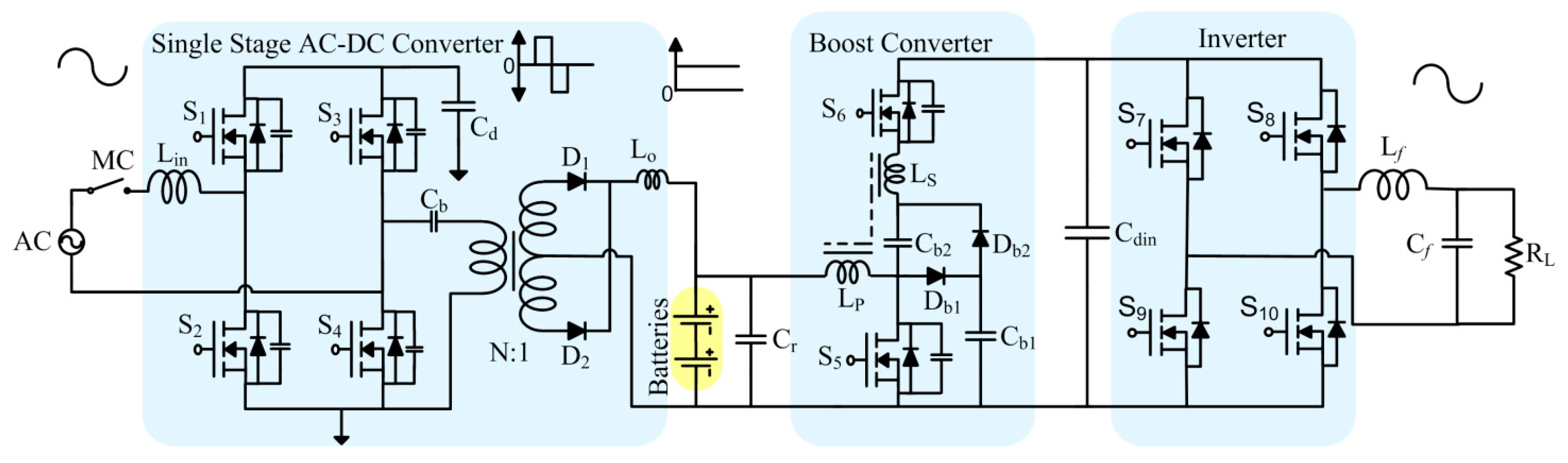
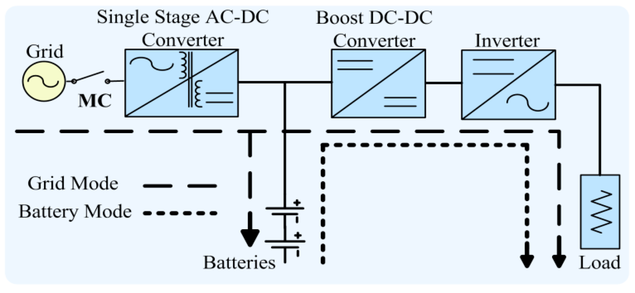
2. Circuit Description

The proposed system consists of a single-stage AC-DC converter at the front end, a H-bridge inverter at the back end, and a high-gain boost converter connected with the battery bank of the UPS system. The single-stage AC-DC converter provides rectification, with power factor correction (PFC) as well as high-frequency isolation between the load and grid. The boost converter with high-voltage gain steps up the low battery bank voltage to high dc-link voltage in order to feed it to the inverter. The H-bridge inverter with a new robust control scheme is proposed for operation under the non-linear loading condition and provides the fast transient response during change of modes.

2.1. Modes of Operation

The UPS operates in two modes, i.e., grid mode and battery mode, as shown in the Figure 2.

2.1.1. Grid Mode

When the grid voltage is stable and there is no power failure, the UPS system operates in grid mode. The single-stage AC-DC converter regulates the voltage across Cr. Meanwhile; the boost converter steps up battery bank voltage across Cr and provides it to the inverter. The inverter provides regulated output voltage to the connected load.

2.1.2. Battery Mode

In case of utility power disruption or any voltage sag, the magnetic contactor (MC) is opened, and the single-stage AC-DC converter stops operation. Now the battery supplies power to the load via the boost converter and inverter connected to it. The arrangement of the battery is such that it provides uninterruptible energy to the boost converter at the time of utility line failure. The value of the dc-link capacitor is kept high in order to provide sufficient energy to the inverter during the transition between the power modes.
A bypass switch has been added in the system to increase the reliability of the system. In case of internal faults in the system or overloading and overheating of the circuit, the bypass switch turns ON and provides a direct path for the power from the utility grid to the connected load [15].

2.2. AC-DC Converter

A number of single-stage AC/DC converters have been proposed in the literature [16,17,18,19,20,21]. Commonly a full bridge diode rectifier has been employed at the front-end of DC/DC converters [22,23,24,25,26], but four diodes operating at line frequency results in high conduction losses, thus dropping the efficiency of the converter. In order to eliminate the aforementioned problems, a bridgeless single-stage PFC AC/DC converter has been implemented in our design.
In [27], a bridgeless single-stage half bridge AC/DC converter has been proposed. It uses only two active switches and two diodes as passive switches to achieve the AC/DC conversion with reduced size and efficient operation. However, the circuit operates in DCM and is not suitable for high power applications. A totem-pole bridgeless PFC connected with high frequency linked DC/DC regulator has been analyzed in [28]. The dc-link capacitor is reduced, which helps in reducing the total cost and size of the system, but the circuit still operates under critical conduction mode of operation.
A single-stage AC/DC converter has been proposed in [29]. The converter operates in continuous condition mode (CCM) and is designed for high power applications, but extra diodes have been used in the circuit which reduces the overall efficiency of the circuit. Also, two separate controllers have been used, which increases the cost and complexity of the circuit.
A new AC-DC converter topology has been introduced, which combines an asymmetrical dc-dc converter with a half bridge PFC rectifier forming a single-stage AC-DC converter. No front end diode rectifier has been used in the circuit. Using the proposed converter, galvanic isolation as well as high efficiency are achieved with only four active switches that reduces the volumetric size of the circuit considerably. Other features of the single-stage converters include continuous conduction of the input and output current, ZVS condition, and excellent input power factor.
The operation of the AC-DC converter in both the positive and negative cycle is symmetrical. Therefore, only the positive cycle is considered in the discussion. Duty cycle D controls the switches S2 and S3, while duty cycle (1-D) controls switches S1 and S4. Figure 3 presents the waveforms and operating modes of the AC-DC converter.

2.2.1. Mode 1

In this mode, switches S2 and S3 turn ON under ZVS conditions. The boost inductor Lin is charged by input AC line voltage Vin through the switch S2 and S3. The inductor current is represented by the following equation:
Δ i L i n = 1 L i n ( V i n + V d ) D T s
The blocking capacitor Cb is charged by the dc-link capacitor Cd through S3 and the secondary side of the high-frequency transformer is fed by the energy stored in the magnetizing inductor Lm. The magnetizing inductor current iLm is represented under the initial condition i L m ( 0 ) by Equation (2):
i L m ( t ) = i L m ( 0 ) + ( V d V b ) D T s L m
The secondary voltage is V s e c 1 = N s N p V p = N s N p ( V d V b ) , V s e c 2 = N s N p ( V d V b ) . The current through the diode D1 is same as the output filter inductor current, and is given as:
i D 1 = i L o ( max ) = i L o ( 0 ) + 1 L o ( N ( V d V b ) V o u t ) D T s

2.2.2. Mode 2

Both the switches S2 and S3 turn OFF during this mode. The parasitic capacitance CS2 is charged and CS1 is discharged using inductor current iLin. Similarly, the capacitance CS3 is charged and capacitance CS4 is discharged by the primary current iP of the transformer.
The voltage across the switches S1 and S4 reduces to zero while the voltage across the switch S2 and S3 increases to Vd. At the secondary side, the output filter inductor current freewheels through the diodes D1 and D2.

2.2.3. Mode 3

In Mode 3, the dc-link film capacitor Cd starts charging by getting energy from the boost inductor and as a result iLin starts decreasing. As the voltage across S1 reduces to 0, the body diode DS1 turns ON. Similarly, the blocking capacitor is fed by the magnetizing inductance Lm through the body diode DS4. As a result, iLm will induce the flux in the high-frequency transformer secondary winding, and the power will be fed to the output capacitor Cr.

2.2.4. Mode 4

In the start of Mode 4, both the switches S1 and S4 turn ON following the ZVS condition. The DC-link capacitor Cd is charged by the stored energy released by the boost inductor Lin. The inductor current is given by:
Δ i L i n = 1 L i n ( V i n V d ) ( 1 D ) T s
The input current flows through Lin, S1, Cd, and S2. Similarly, the magnetising current iLm starts decreasing from maximum as represented by the following Equation (5):
i L m ( t ) = i L m ( max ) V b L m ( 1 D ) T s
The high-frequency transformer secondary winding feed energy to the output capacitor D2. The output filter inductor current iLO is represented by Equation (6):
i L o = i L o ( t ) = i L o ( 0 ) 1 L o N ( V d V b ) ( 1 D ) T s

2.2.5. Mode 5

In Mode 5, the switches S1 and S4 turn OFF. The parasitic capacitor CS2 is discharged and CS1 is charged by both the current from the transformer primary windings and the input inductor Lin to and from Vd, respectively. Now the voltage across S2 is zero, and the voltage across S1 is Vd. Similarly, the capacitance CS4 is charged and CS3 is discharged by the primary current iP of the transformer. Thus, the voltage across S4 is Vd. At the secondary side, the output filter current freewheels through the diode D1 and D2.

2.2.6. Mode 6

In Mode 6, the body diode DS2 turns ON because of charging of the inductor. Similarly, the voltage across the switch S3 is zero. This causes the body diode DS3 to be turned ON and the primary current starts flowing through it. In the end of Mode 6, both the S2 and S3 turn ON under the condition of ZVS.

2.2.7. Continuous condition mode (CCM) of operation of input inductor

The proposed AC-DC converter operates in CCM with continuous input current. The minimum inductor for CCM operation can be determined by (7):
L i n > V d 2 T s D ( 1 D ) 2 2 P o
The average current ripple is given by Equation (8):
Δ i L i n = | V m sin ω t | D T s 2 L i n
The peak current is given by (9):
i L i n | p e a k = i L i n ( a v g ) + Δ i L i n = | V m sin ω t | R e + | V m sin ω t | D T s 2 L i n
where Re is the emulative resistance of the converter. Equation (9) shows that the inductor peak current is not very high because large value of inductor is selected which maintains the continuous conduction.

2.2.8. Discontinuous conduction mode (DCM) of operation of the input inductor

If the proposed UPS system is designed for low power applications, the input inductor can be operated in discontinuous conduction mode [30]. The peak boost inductor current follows the line voltage with a fixed duty ratio to supply the output power for a constant output voltage. Suppose the converter is lossless and the duty ratio is fixed, the boost inductor Lb should be determined by (10):
L i n < V i n 2 D T s 2 P o
where Po is the maximum output power. For positive line period, the peak boost inductor current during TS is expressed as (11):
i L b ,   p e a k = V i n D T s L b

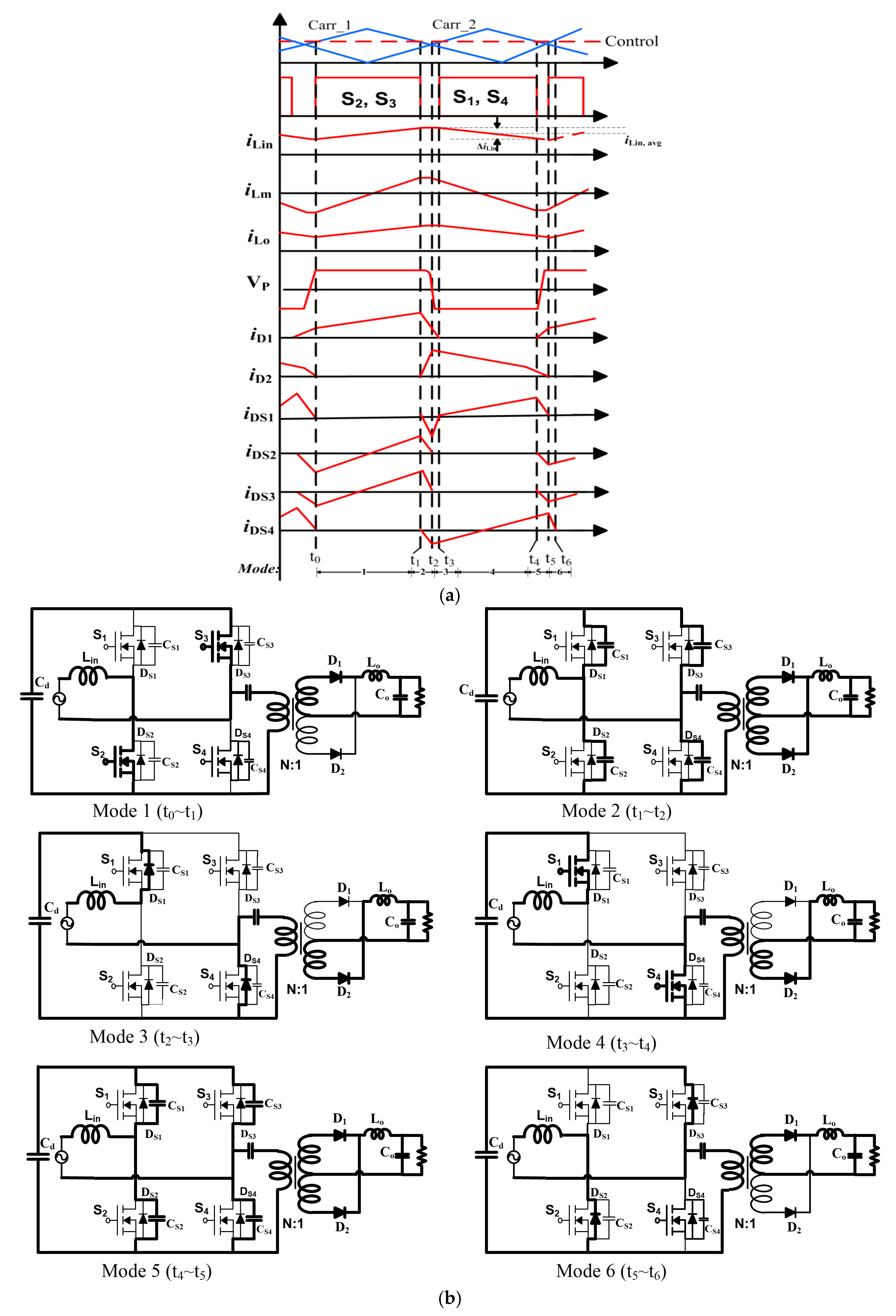
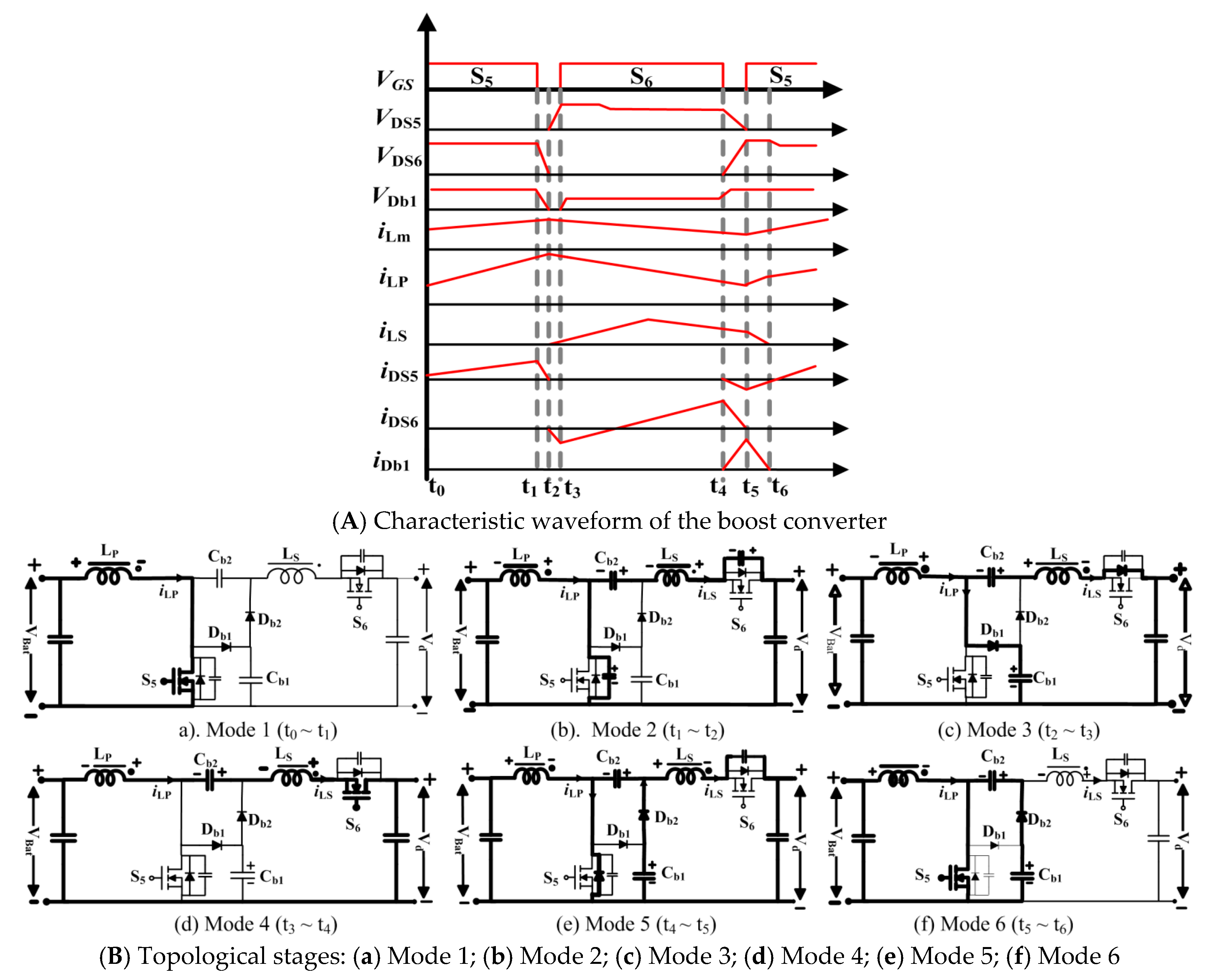
2.3. Boost Converter

A high-gain DC-DC converter has been introduced to obtain high dc-link voltage from the low voltage battery bank [31]. SR has been applied to decrease the conduction losses and force the circuit to operate under ZVS conduction. In order to get the high-voltage gain, coupled inductor is utilized with LP and LS as primary and secondary winding inductance respectively. The characteristic waveform and modes of operation of the DC-DC converter is shown in the Figure 4.

2.3.1. Mode 1 (t0~t1)

During Mode 1, the switch S5 is ON, while the switch S6 is OFF. Low battery bank voltage is applied at the input of the DC-DC boost converter. Capacitor Cb2 remains charged before Mode 1 and the magnetizing current iLm of the coupled inductor increases linearly, as shown in the Figure 5.
Applying KVL, we get:
V L = V L p = V L S / N
The voltage across the primary winding can be find using voltage second balance:
V L P ( 1 D ) = V L D

2.3.2. Mode 2 (t1~t2)

The switch S5 turns OFF in Mode 2. The primary current iLP charges the parasitic capacitance across the switch S5 and the secondary current iLS discharges the parasitic capacitance across switch S6. When the voltage across switch S5 equals to the capacitor voltage VCb1, this mode finishes.

2.3.3. Mode 3 (t2~t3)

Since the switch S5 is OFF, the primary current iLP decreases due to leakage inductance. However, the secondary current iLS increases, which results in the turning ON of the body diode of switch S6. As the voltage across the switch S5 is higher than capacitor Cb1, it charges Cb1 through diode Db1. Hence, the voltage stress across the switch S5 has been reduced. VCb1 is the voltage across the capacitor Cb1, and is represented by Equation (14):
V Cb 1 = V L + V L P
Using (13):
V Cb 1 = V L / ( 1 D )

2.3.4. Mode 4 (t3~t4)

In Mode 4, the switch S6 turns ON under ZVS conditions. Both the windings of the coupled inductor and the capacitor Cb2 series connected together transfer maximum energy to the output capacitor Cdin of the converter. The iLS starts increasing until it reaches the iLP, then it follows the iLP till the end of the Mode 4. Thus, the energy stored in both the windings of the coupled inductor discharges across the high voltage side of the circuit. Db1 and Db2 are reverse biased during this mode. Applying voltage second balance, we get Equation (16):
V H = V L + V L S + V Cb 2 + V L p
V H = V L + V Cb 2 + ( N + 1 ) V L P

2.3.5. Mode 5 (t4~t5)

During this mode, the switch S6 turns OFF. The current iLS charges the parasitic capacitance of the switch S6. Capacitor Cb2 is charged by the capacitor Cb1 through the diode Db2:
V Cb 2 = V Cb 1 = V L / ( 1 D )
By substituting (13) and (18) into (17), presents the voltage gain of the converter:
V H = V L + V L / ( 1 D ) + ( N + 1 ) D / ( 1 D ) V L
G b o o s t = V H / V L = ( 2 + N D ) / ( 1 D )
The body diode of the switch S5 turns ON because of the polarities of capacitor Cb2 and inductor LP.

2.3.6. Mode 6 (t5~t6)
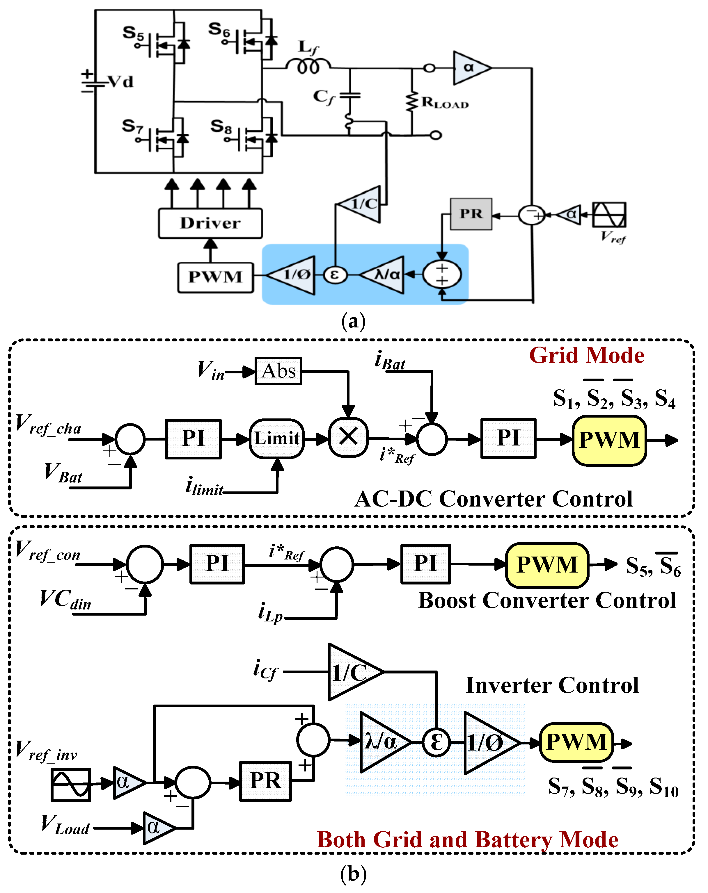
During this mode, the switch S5 turns to ON state under ZVS conditions. Since no current is derived by switch S5 from the clamped circuit, thus the switching losses remains low due to ZVS, results in increasing the efficiency of the converter. Mode 6 finishes at the point when both the VCb1 and VCb2 become equal. The turn ratio N = 4 is selected to satisfy the Gboost gain in order to step up the battery bank voltage to required dc-link of inverter.

3. Control Strategy

The control schemes for regulating different parts of the proposed UPS, in different modes of operation are shown in Figure 5. The control scheme for inverter and boost converter keeps operating in both the normal and battery powered mode. On the other hand, for a single-stage converter the control scheme operates only in normal mode of operation for charging the battery as well as supplying power to the boost converter.

3.1. Inverter Control

A conventional full bridge voltage source inverter has been used to perform DC to AC conversion. SM control is famous for its excellent performance against non-linear loading conditions. SMC is also robust in operation and easy to implement for a full bridge inverter. In order to control the output voltage of the inverter, cascaded control algorithm of SMC and PR has been proposed for the control of inverter. The inner current loop is controlled by the SM control while the outer voltage loop is controlled by the PR control. Smoothed control law in narrow boundary layer has been used to eliminate the phenomena of chattering SMC. The smoothed control law is applied to the pulse width modulator that results in the fixed switching frequency of the inverter. Thus, the proposed controller adopted the characteristic of both SMC and PR control.
The circuit diagram of a single phase inverter with LC filter and proposed controller for non-linear load is shown in Figure 5a, where Vd is the applied DC-link voltage, Vout the filter capacitor Cf output voltage. iLf is the inductor Lf current and io the output current through the load R, given by io = Vout/RLoad. The state equations of the inverter are given as:
d d t [ V o u t i L f ] = [ 0 1 C f 1 L f 0 ] [ V o u t i L f ] + [ 0 V d L f ] u + [ 0 i o C f ]
where u = C o n t r o l   i n p u t = { 1 ,   0 ,   + 1 } .
In order to implement the sliding mode control, the voltage error x1, and its derivative x 2 = x ˙ 1 need to be find:
x 1 = V o u t V r e f
x 2 = x ˙ 1 = V ˙ o u t V ˙ r e f = i C f C f V ˙ r e f
where V r e f = V m sin ( ω t ) . Consider the slide surface equation:
S = λ x 1 + x 2
Now to apply the sliding control law to the inverter, putting the value of x1 and x2:
S = λ ( V o u t V r e f ) + i C f C f V ˙ r e f
S = λ ( V o u t V r e f ) + 1 C f ( i C f i r e f )
The sliding mode controller has the common inherent property of chattering. Chattering affects the control accuracy and reduces the efficiency of the circuit. In order to overcome the chattering, a smoothed SM control has been implemented. This can be achieved by smoothing out the control discontinuity in a thin boundary layer neighboring the sliding surface:
B ( t ) = { x , | S ( x ; t ) | }   > 0
where is the boundary layer thickness and ε = λ is the boundary layer width. Hence, interpolating S inside B ( t ) , for instance, and replacing S by an expression S/ , Equation (26) will be:
S ( x ) = λ [ V o u t V r e f ] + 1 C f [ i C f i r e f ]
The smoothing control discontinuity assigns a low pass filter structure to the local dynamics thus eliminating chattering. The control law needs to be tuned very precisely in order to achieve a trade-off between the tracking precision and robustness to the uncontrolled dynamics. Hence, the final equation for the control of the inverter can be derived by combining the proportional resonant control and SM control for the current loop:
S ( x ) = 1 C   [ i C i r e f ] + λ [ K p ( V o u t V r e f ) + k i ( 2 s s 2 + 2 ω c s + ω o 2 ) ( V o u t V r e f ) ]
Thus Equation (29) shows the dynamic behavior in both SM and PR compensator control. The error in the voltage loop is compensated by the appropriate PR parameters, thus, the output voltage is compelled to follow the reference AC voltage leading to system stability while the SMC drives the system to the zero sliding surface with maximum stability. Since the capacitor error current contains the ripples from the inductor, the current peak may reach high values, so should be carefully assigned a value in order to compensate the slope from the high current ripple of the capacitor. Hence, the PR controller eliminates the steady-state error at resonant frequency or harmonic at that frequency. The response time of the system λ determines the dynamics and robustness of the system. It is clear from Equation (29), that a smaller value of λ leads to a slow response time, while higher λ values though increase the response time, but take a longer time to reach the sliding surface. Thus the optimal value for λ is equal to the switching frequency of the inverter.
According to [32], the slope of the carrier wave is 4 V m × f s , where V m is the magnitude and fs is the frequency of carrier wave. The slope of the error signal to the modulator is given by V D C / 4 L C . According to the limitation of the pulse width modulator, slope of error signal < slope of the carrier signal:
4 V m × f s < V D C 4 L C
Thus, the minimum value of can be calculated using (30):
10 V D C 16 L C V m f S
Table 2 shows the comparison of the proposed control scheme with the SM control and other common controllers. The proposed controller shows an improvement in terms of reducing the THD and transient response (TS) with robust control of the inverter.

3.2. Battery Charger Control

The AC-DC converter of the UPS system acts as a battery charger as shown in Figure 5. In this control scheme, the faster inner current loop regulates the inductor current so that its average value during each period follows the rectified input voltage. The slower outer voltage loop maintains the battery voltage close to reference voltage and generates the control signal for the current loop. The steady state analysis of the AC-DC converter shows stable performance during grid mode. The state space equations of the rectifier are derived as:
d i L d t = V i n L i n D + ( V i n V d ) L i n ( 1 D )
d v d d t = V d R C d D + ( i L C d V d R C d ) ( 1 D )
Assuming the current loop has high bandwidth as compared to the voltage loop, and dc-link capacitor Cd is large enough to give approximately constant voltage i.e., d v d / d t = 0 . With V ^ i n = 0 , the small signal control d ^ to input current i ^ L transfer function G i L d ( s ) of the inner current loop is give by:
G i L d ( s ) = i ^ L d ^ = V d s ( L i n )
The stability of the current loop depends on the current loop gain, hence a suitable proportional-integral (PI) controller G i ( s ) = k p i + k i i s , is used for compensating the current loop. The Bode plot of the current loop gain T i = G i L d ( s ) · G i ( s ) is obtained considering the circuit parameters shown in Table 4. The values of the proportional gain Kpi and integral gain Kii are selected as 2.3 and 1200, respectively, for the stable operation of the current loop. Figure 6a presents the Bode plot of the current loop gain with phase margin of 89° and stable operation of the rectifier.
The same approach is used to compensate the voltage loop of the average current control scheme. v ^ c is the reference current for the current loop. Assuming constant input voltage, the small signal control v ^ c to output transfer function G V d V c ( s ) of the voltage loop is derived as:
G V d V c ( s ) = v ^ d v ^ c = V i n R 2 V d ( s C R + 2 )
In order to force the output voltage to follow the reference voltage VRef, a proportional-integral (PI) compensator has been employed. Combining the power stage with the PI controller G v ( s ) = k p v + k i v s provides the overall loop gain.
T v = G v . G V d V c ( s ) of the voltage loop. The values of Kpv and Kiv in voltage loop are selected as 1.2 and 13, respectively. The stability of the voltage loop can be analyzed using the Bode plot obtained by considering the parameters from Table 4, as shown in Figure 6b. The system shows good stability with a positive phase margin.
In charging mode, the controller operates as constant current mode CC or constant voltage mode CV depending on the battery voltage as shown in the Figure 5b. In current loop, the battery input current iBat is forced to follow the reference current iRef using a PI compensator in (36):
i * = K p ( i R e f i B a t ) + K i ( i R e f i B a t ) d t
Similarly, the battery voltage is regulated by the voltage loop using the PI compensator that forces the output battery voltage VBat to follow the reference voltage Vref. The current limiter is introduced to limit the maximum charging current of the battery. If the iref is greater than ilimit, the battery is charged at constant current (CC Mode), in contrast if the iref is less than ilimit, the battery is charged at constant voltage (CV mode).

3.3. Boost Converter Control

The steady state analysis of the boost converter is performed using average state variable method [30]. The state space equation for the converter with coupled inductor is derived as:
d i P d t = V B a t d t D + ( V B a t V d ) L m ( N + 1 ) ( 1 D )
d V o d t = i p C ( N + 1 ) ( 1 D ) V o R C
Now we perturb the system and consider only the dynamic terms and eliminate the product of the AC terms because of very small value. The final equation after Laplace transform is:
s v ^ o = i ^ P ( 1 D C ( N + 1 ) ) v ^ d R C I P C ( N + 1 ) d ^
s i ^ P = v ^ B a t ( D L m + 1 D L m ( N + 1 ) ) v ^ d ( 1 D L m ( N + 1 ) ) + d ^ ( V B a t L m V B a t + V d L m ( N + 1 ) )
Solving (37) and (38) gives the transfer function of the converter:
v ^ o d ^ = s ( I P C ( N + 1 ) ) + ( 1 D ) C ( N + 1 ) ( V B a t L m + V d V B a t L m ( N + 1 ) ) s 2 + s 1 R C + ( 1 D ) 2 ( 1 + N ) 2 L m C
Considering the gain due to clamp capacitor Cb2, the transfer equation is given by:
v ^ o d ^ = s ( I P C ( N + 1 ) ) + ( 1 D ) C ( N + 1 ) ( V B a t L m + V d V B a t ( D / 1 D ) L m ( N + 1 ) ) s 2 + s 1 R C + ( 1 D ) 2 ( 1 + N ) 2 L m C
The stability of the converter can be analyzed using the Bode plot shown in Figure 7. The system shows good stability with a positive phase margin and it has no right half plane poles. It is easy to achieve high crossover frequencies by adjusting a suitable gain of the compensators as the phase never reaches −180. The voltage across DC-link capacitor Cdin is regulated by using a suitable voltage compensator [37]. The PI compensator is used to track the DC-link voltage Vd to follow the reference voltage, as shown in Figure 7.

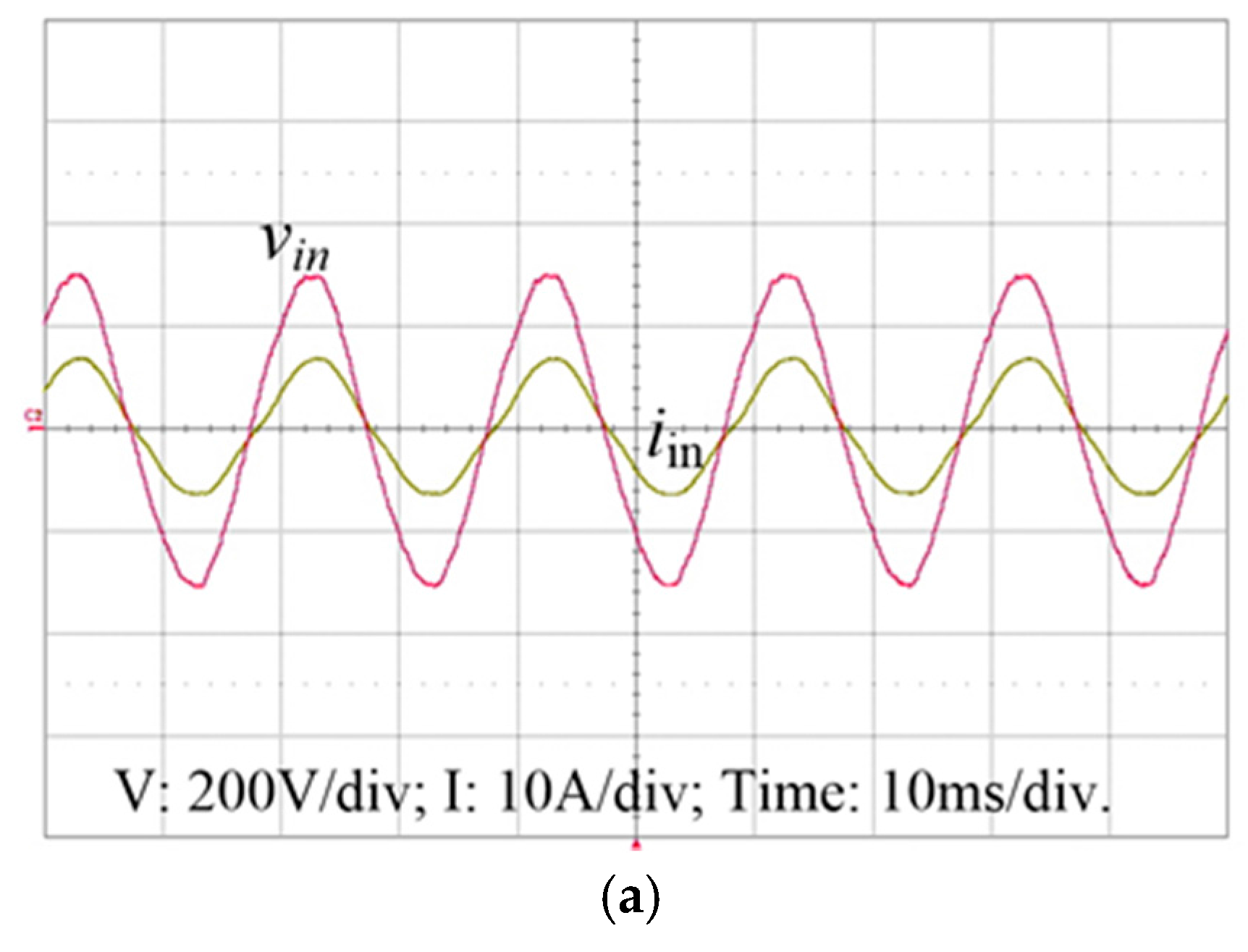
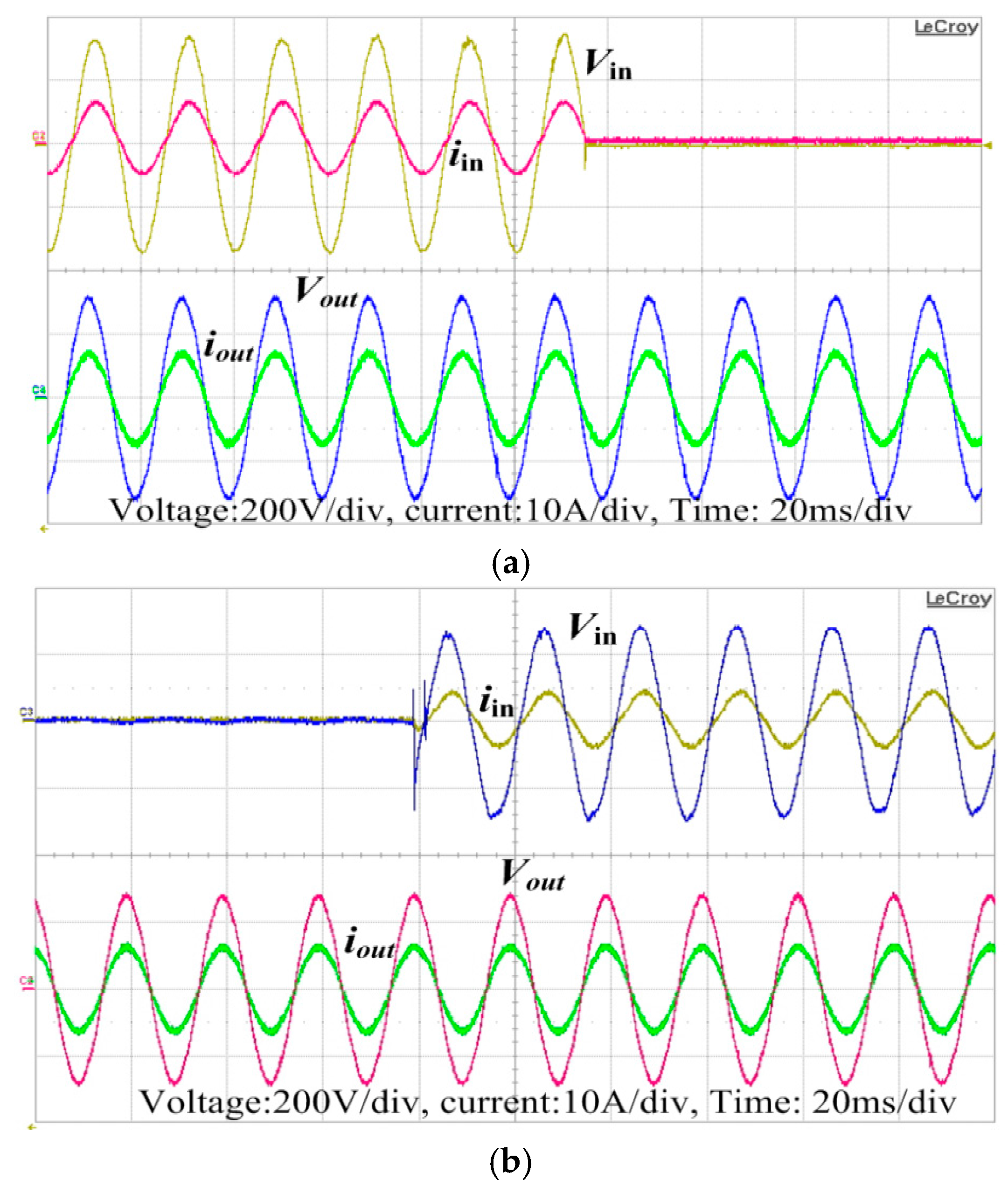
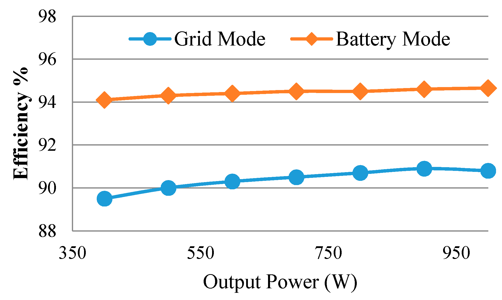
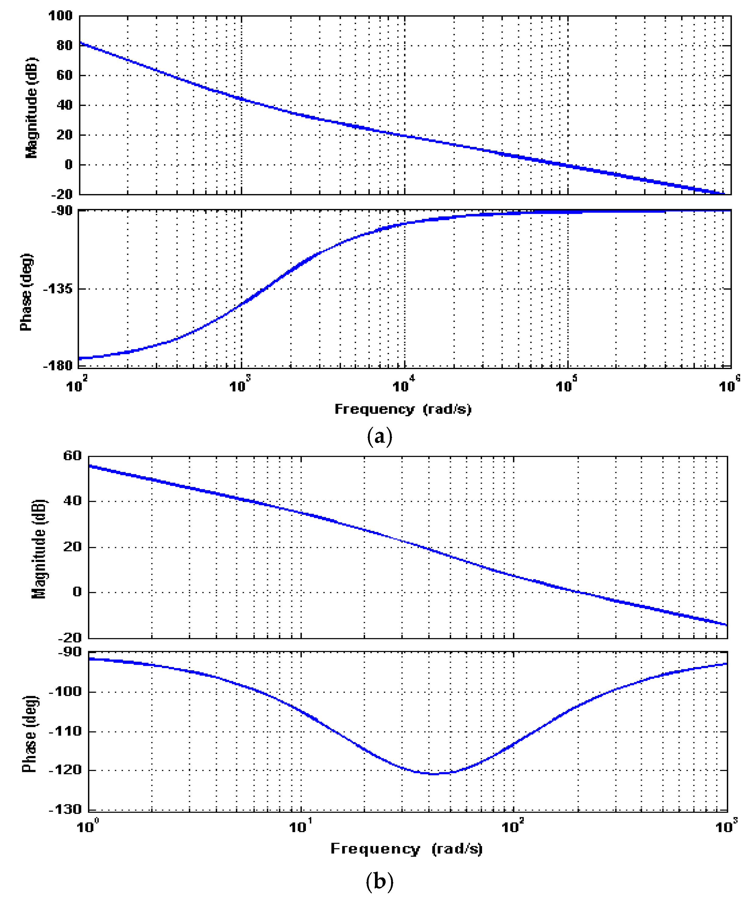
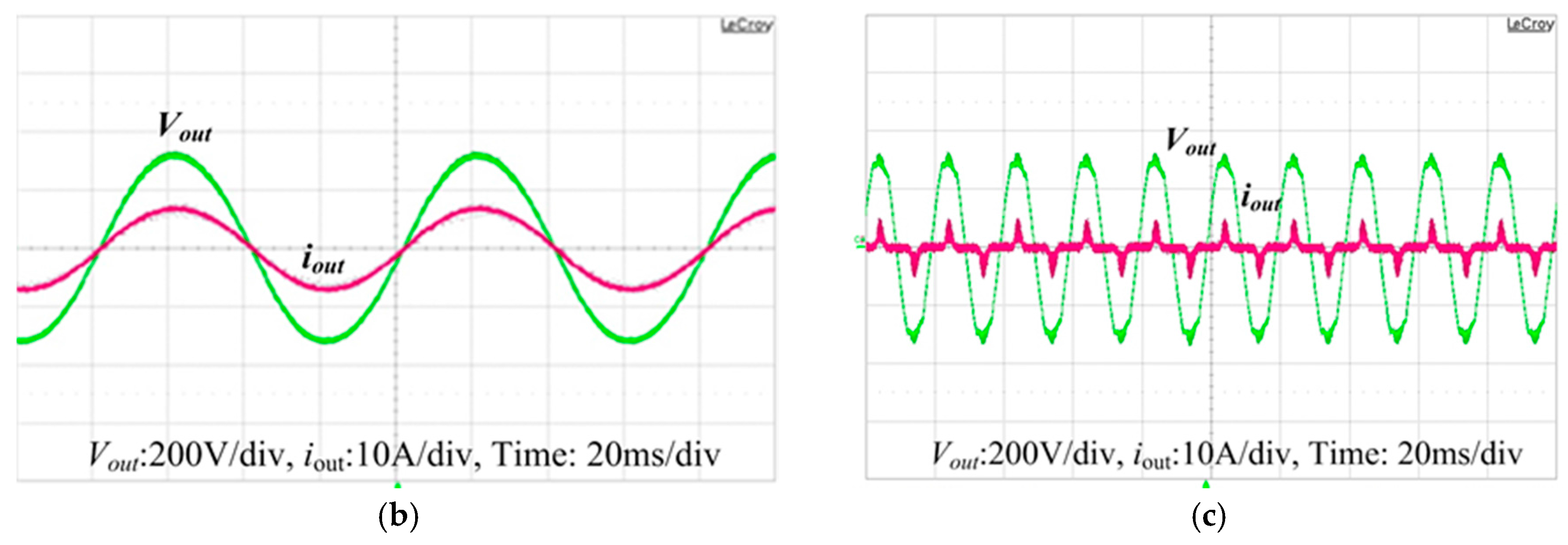
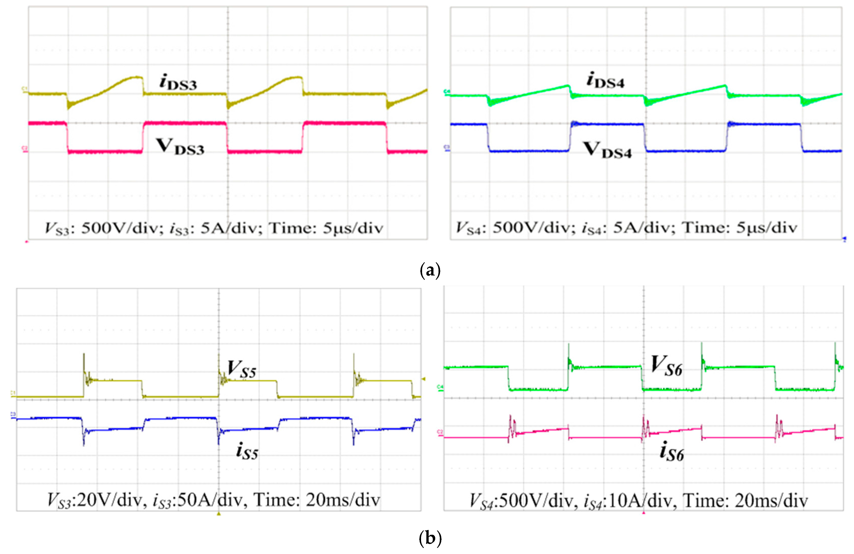
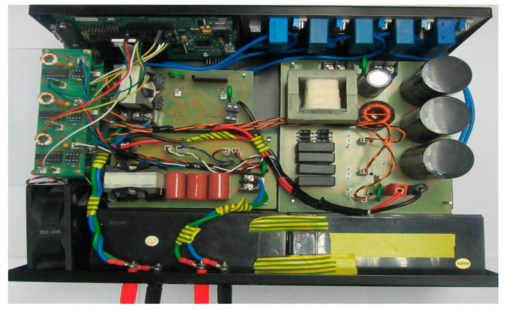
4. Experimental Results

In order to validate the performance of our UPS system, a laboratory prototype has been implemented. The specifications of the UPS are shown in Table 3. The control scheme for the single-stage converter, boost converter, and H-bridge inverter has been implemented using DSP TMS320F28335. The design parameters of the single-stage converter and DC-DC converter are shown in Table 4 and Table 5, respectively. The backup storage system consists of two batteries (each battery is 24 V/35 Ah), or parallel batteries, depending upon the backup time for the connected load.
The utility input voltage and current waveform in normal mode of operation is shown in Figure 8a. The input is sinusoidal, with unity power factor and THD less than 5%. The output voltage and current waveform during linear loads and non-linear load are shown in Figure 8b,c. The waveform is sinusoidal for linear loads with THD less than 1%. For a non-linear load designed according to the standard of IEC62040-3, the THD is 1.25% [38].
Figure 9a shows the drain to source voltage and current of the switches S3 and S4. Both the switches are operating under the condition of ZVS. Figure 9b shows the drain to source voltage of the switches S5 and S6 of the boost converter. Both switches are operating under the condition of ZVS. Also the voltage stress across the switches is also limited. When the grid power is interrupted, the system switches from grid mode to battery mode. The rectifier is no longer in operation and the boost converter provides regulated dc-link voltage.
The transient effect in the output voltage is very small and the UPS system provides uninterruptible power to the load as shown in Figure 10a. Similarly, the transition from battery mode back to grid mode upon the restoration of the grid power is shown in Figure 10b. There is a small transient at the turning ON point of the AC-DC converter. This transient is due to the inductor which remains charged due to previous grid mode of operation. However the small transient can be controlled by a suitable snubber circuit. Figure 10 also shows that the inverter keeps operating in both the grid and battery powered mode of operation and the load is getting power without any interruption. Figure 11 shows a photograph of our laboratory prototype. Figure 12 shows the efficiency graph with maximum efficiency of 95% during battery mode and 91% during grid mode of operation. Thus utilizing soft switching in boost converter reduces the switch losses and increases the efficiency of the system. The efficiency in battery mode is high as compared to grid mode because less number of power stages are operation during this mode. Table 6 shows a comparison of the different high-frequency transformer isolated UPS systems. The proposed UPS shows a distinct improvement in terms of increasing the efficiency, reducing the size of the battery bank, and decreasing the volumetric size and weight of the system.

5. Conclusions

A single phase high-frequency transformer isolated online UPS has been proposed in this paper. A single-stage AC-DC converter provides galvanic isolation, efficient power conversion, and excellent power factor correction. Besides, the AC-DC converter also charges the battery bank of the UPS system during grid mode of operation. When there is a grid interruption, the low battery bank voltage is raised to high dc-link voltage using a boost converter which reduces the battery bank significantly. The boost converter provides high voltage gain with less number of active switches. A new inverter control of cascaded PR and SM control is used which provides regulated sinusoidal output voltage with low THD for both linear and non-linear load. Overall, the volume of the system is minimized by reducing the size, weight, and battery bank of the system. The experimental results show good dynamic and steady state performance.

Authors Contribution

All the authors contributed in finalizing the Paper. The main idea of the paper was presented by Muhammad Aamir while Wajaht Ullah Tareen and Kafeel Ahmed Kalwar helped in the control of the circuit. Mudasser Ahmed Memon prepared the format of the paper. Saad Mekhilef is the head of research team.

Acknowledgments

The authors would like to acknowledge the financial support from Bahria University, Islamabad, Pakistan.

Conflicts of Interest

The authors declare no conflict of interest.

References

  1. Lahyani, A.; Venet, P.; Guermazi, A.; Troudi, A. Battery/supercapacitors combination in uninterruptible power supply (UPS). IEEE Trans. Power Electron. 2013, 28, 1509–1522. [Google Scholar] [CrossRef]
  2. Zhao, B.; Song, Q.; Liu, W.; Xiao, Y. Next-generation multi-functional modular intelligent UPS system for smart grid. IEEE Trans. Ind. Electron. 2013, 60, 3602–3618. [Google Scholar] [CrossRef]
  3. Branco, C.G.; Torrico-Bascope, R.P.; Cruz, C.M.; de A Lima, F. Proposal of three-phase high-frequency transformer isolation UPS topologies for distributed generation applications. IEEE Trans. Ind. Electron. 2013, 60, 1520–1531. [Google Scholar] [CrossRef]
  4. Hwang, J.-C.; Chen, J.-C.; Pan, J.-S.; Huang, Y.-C. Measurement method for online battery early faults precaution in uninterrupted power supply system. IET Electr. Power Appl. 2011, 5, 267–274. [Google Scholar] [CrossRef]
  5. Karve, S. Three of a kind [UPS topologies, IEC standard]. IEE Rev. 2000, 46, 27–31. [Google Scholar] [CrossRef]
  6. Vázquez, N.; Villegas-Saucillo, J.; Hernández, C.; Rodríguez, E.; Arau, J. Two-stage uninterruptible power supply with high power factor. IEEE Trans. Ind. Electron. 2008, 55, 2954–2962. [Google Scholar]
  7. Aamir, M.; Kafeel, A.K.; Mekhilef, S. Review: Uninterruptible power supply (UPS) system. Renew. Sust. Energy Rev. 2016, 58, 1395–1410. [Google Scholar] [CrossRef]
  8. Rodriguez, E.; Vázquez, N.; Hernández, C.; Correa, J. A novel AC UPS with high power factor and fast dynamic response. IEEE Trans. Ind. Electron. 2008, 55, 2963–2973. [Google Scholar] [CrossRef]
  9. Torrico-Bascope, R.P.; Oliveira, D.S.; Branco, C.G.C.; Antunes, F.L.M. A UPS with 110-V/220-V input voltage and high-frequency transformer isolation. IEEE Trans. Ind. Electron. 2008, 55, 2984–2996. [Google Scholar] [CrossRef]
  10. Nasiri, A.; Nie, Z.; Bekiarov, S.B.; Emadi, A. An on-line UPS system with power factor correction and electric isolation using BIFRED converter. IEEE Trans. Ind. Electron. 2008, 55, 722–730. [Google Scholar] [CrossRef]
  11. Hirachi, K.; Yoshitsugu, J.; Nishimura, K.; Chibani, A.; Nakaoka, M. Switched-mode PFC rectifier with high-frequency transformer link for high-power density single phase UPS. In Proceedings of the IEEE 28th Annual IEEE Power Electronics Specialists Conference, (PESC’97 Record), St. Louis, MO, USA, 27 June 1997; Volume 1, pp. 290–296. [Google Scholar]
  12. De Rooij, M.A.; Ferreira, J.A.; van Wyk, D. A novel unity power factor low-EMI uninterruptible power supply. IEEE Trans. Ind. Electron. 1998, 34, 870–877. [Google Scholar] [CrossRef]
  13. Park, H.S.; Kim, C.H.; Park, K.B.; Moon, G.W.; Lee, J.H. Design of a charge equalizer based on battery modularization. IEEE Trans. Veh. Technol. 2009, 58, 3216–3223. [Google Scholar] [CrossRef]
  14. Lee, Y.S.; Cheng, M.W. Intelligent control battery equalization for series connected lithium-ion battery strings. IEEE Trans. Ind. Electron. 2005, 52, 1297–1307. [Google Scholar] [CrossRef]
  15. Zhang, Y.; Yu, M.; Liu, F.; Kang, Y. Instantaneous current-sharing control strategy for parallel operation of UPS modules using virtual impedance. IEEE Trans. Power Electron. 2013, 28, 432–440. [Google Scholar] [CrossRef]
  16. Yang, S.; Chen, S.; Lin, J. Dynamics analysis of a low-voltage stress single-stage high-power factor correction AC/DC flyback converter. IET Power Electron. 2012, 5, 1624–1633. [Google Scholar] [CrossRef]
  17. Duarte, J.; Lima, L.R.; Oliveira, L.; Michels, L.; Rech, C.; Mezaroba, M. Single-stage high power factor step-up/step-down isolated AC/DC converter. IET Power Electron. 2012, 5, 1351–1358. [Google Scholar] [CrossRef]
  18. Ki, S.; Lu, D. Extension of minimum separable switching configuration modelling to single-stage AC/DC converters with direct power transfer. IET Power Electron. 2012, 5, 1154–1163. [Google Scholar] [CrossRef]
  19. Yang, L.-S.; Liang, T.-J.; Chen, J.-F.; Lin, R.-L. Analysis and design of a novel, single-stage, three-phase AC/DC step-down converter with electrical isolation. IET Power Electron. 2008, 1, 154–163. [Google Scholar] [CrossRef]
  20. Ma, H.; Ji, Y.; Xu, Y. Design and analysis of single-stage power factor correction converter with a feedback winding. IEEE Trans. Power Electron. 2010, 25, 1460–1470. [Google Scholar] [CrossRef]
  21. Mahdavi, M.; Farzaneh-Fard, H. Bridgeless CUK power factor correction rectifier with reduced conduction losses. IET Power Electron. 2012, 5, 1733–1740. [Google Scholar] [CrossRef]
  22. Abasian, A.; Farzaneh-fard, H.; Madani, S. Single stage soft switching AC/DC converter without any extra switch. IET Power Electron. 2014, 7, 745–752. [Google Scholar] [CrossRef]
  23. Liang, T.-J.; Yang, L.-S.; Chen, J.-F. Analysis and design of a single-phase AC/DC step-down converter for universal input voltage. IET Electr. Power Appl. 2007, 1, 778–784. [Google Scholar] [CrossRef]
  24. Lai, C.; Shyu, K. A single-stage AC/DC converter based on zero voltage switching LLC resonant topology. IET Electr. Power Appl. 2007, 1, 743–752. [Google Scholar] [CrossRef]
  25. Lin, J.-L.; Yao, W.-K.; Yang, S.-P. Analysis and design for a novel single-stage high power factor correction diagonal half-bridge forward AC/DC converter. IEEE Trans. Circ. Syst. I Regul. Pap. 2006, 53, 2274–2286. [Google Scholar] [CrossRef]
  26. Lu, D.-C.; Iu, H.-C.; Pjevalica, V. Single-stage AC/DC boost–forward converter with high power factor and regulated bus and output voltages. IEEE Trans. Ind. Electron. 2009, 56, 2128–2132. [Google Scholar] [CrossRef]
  27. Choi, W.-Y.; Yoo, J.-S. A bridgeless single-stage half-bridge AC/DC converter. IEEE Trans. Power Electron. 2011, 26, 3884–3895. [Google Scholar] [CrossRef]
  28. Ribeiro, H.S.; Borges, B.V. High-performance voltage-fed AC–DC full-bridge single-stage power factor correctors with a reduced DC bus capacitor. IEEE Trans. Power Electron. 2014, 29, 2680–2692. [Google Scholar] [CrossRef]
  29. Das, P.; Pahlevaninezhad, M.; Moschopoulos, G. Analysis and design of a new AC–DC single-stage full-bridge PWM converter with two controllers. IEEE Trans. Ind. Electron. 2013, 60, 4930–4946. [Google Scholar] [CrossRef]
  30. Erickson, R.W.; Maksimovic, D. Fundamentals of Power Electronics; Springer Science & Business Media: New York, NY, USA, 2001. [Google Scholar]
  31. Aamir, M.; Mekhilef, S.; Hee-Jun, K. High-gain zero-voltage switching bidirectional converter with a reduced number of switches. IEEE Trans. Circ. Syst. II Express Briefs 2015, 62, 816–820. [Google Scholar] [CrossRef]
  32. Zargari, N.; Ziogas, P.; Joos, G. A two switch high performance current regulated DC/AC converter module. IEEE Trans. Ind. Appl. 1995, 31, 583–589. [Google Scholar] [CrossRef]
  33. Cortes, P.; Ortiz, G.; Yuz, J.I.; Rodriguez, J.; Vazquez, S.; Franquelo, L.G. Model predictive control of an inverter with output LC filter for UPS applications. IEEE Trans. Ind. Electron. 2009, 56, 1875–1883. [Google Scholar] [CrossRef]
  34. Tamyurek, B. A high-performance SPWM controller for three-phase UPS systems operating under highly nonlinear loads. IEEE Trans. Power Electron. 2013, 28, 3689–3701. [Google Scholar] [CrossRef]
  35. Komurcugil, H. Rotating-sliding-line-based sliding-mode control for single-phase UPS inverters. IEEE Trans. Ind. Electron. 2012, 59, 3719–3726. [Google Scholar] [CrossRef]
  36. Abrishamifar, A.; Ahmad, A.A.; Mohamadian, M. Fixed switching frequency sliding mode control for single-phase unipolar inverters. IEEE Trans. Power Electron. 2012, 27, 2507–2514. [Google Scholar] [CrossRef]
  37. Ullah, W.; Mekhilef, S. Transformer-less 3P3W SAPF (three-phase three-wire shunt active power filter) with line-interactive UPS (uninterruptible power supply) and battery energy storage stage. Energy 2016, 109, 525–536. [Google Scholar]
  38. International Electro-technical Commission. Uninterruptible Power Systems (UPS)—Methods of Specifying the Performance and Test Requirements; IEC62040-3 Standard; IEC: Geneva, Switzerland, 1999. [Google Scholar]
Figure 1. Circuit diagram of the proposed UPS system.
Energies 10 00418 g001
Figure 2. Modes of operation of proposed UPS system.
Energies 10 00418 g002
Figure 3. Single-stage AC-DC Converter: (a) Operation waveforms; (b) Modes of operation during one switching cycle TS.
Energies 10 00418 g003
Figure 4. DC-DC boost converter; (A) Characteristic waveform; (B) Topological stages.
Energies 10 00418 g004
Figure 5. Proposed control scheme: (a) Inverter control; (b) Control circuit UPS system.
Energies 10 00418 g005
Figure 6. Bode response of rectifier; (a) Current loop gain; (b) Voltage loop gain.
Energies 10 00418 g006
Figure 7. Bode plot of the boost converter.
Energies 10 00418 g007
Figure 8. Experimental waveform of the input output voltage and current of the UPS system. (a) Input line voltage and current; (b) Inverter with linear Load; (c) Inverter with Non-linear load.
Energies 10 00418 g008aEnergies 10 00418 g008b
Figure 9. Drain to source voltage and current of the switches. (a) S3 and S4 of single-stage AC-DC Converter; (b) S5 and S6 of boost DC-DC converter.
Energies 10 00418 g009
Figure 10. Transition between two modes of operation, Input voltage Vin and current Iin, Output voltage Vout and current Iout. (a) Grid to battery mode and (b) Battery mode to grid mode.
Energies 10 00418 g010
Figure 11. Laboratory prototype.
Energies 10 00418 g011
Figure 12. Efficiency graph of UPS in grid and battery mode.
Energies 10 00418 g012
Table 1. Comparison of high-frequency transformer UPSs for different battery banks.
ReferenceRated PowerInput/Output VoltageBattery Bank VoltageNumber of Batteries
[8]300 VA120484
[9]2 kVA2201089
[10]150 VA120484
[11]2 kVA11018015
[12]3.3 kVA22012010
Table 2. Comparison of different control methods.
ParametersModel Predictive Control [33]SPWM Control [34]Rotating SMC [35]Fix-Freq SMC [36]Proposed Work
VDC529405300360350
VRMS150220200220220
Cf (uF)402021009.46.6
Lf (mH)2.40.030.2500.3570.84
THD (L)2.85%1.11%-1.1%0.45%
THD (NL)3.8%3.8%2.66%1.7%1.25%
TS (ms)5060-0.50.3
Table 3. Specifications of the proposed UPS system.
ParametersSymbolValue
Input VoltageVin220 V
Output VoltageVout220 V
Grid Frequencyfr50 Hz
Output Frequencyfo50 Hz
Number of BatteriesVb2 Parallel connected (24 V/35 Ah)
Maximum Output PowerPo,max1 kVA
DC-link VoltageVd360 V
Table 4. Design parameters of the single-stage AC-DC converter.
ParametersSymbolValue
Input InductorLin1.2 mH
SwitchesS1~S4SPP11N60C3
Fast DiodesD1, D2C3D10060A
Switching frequencyfs50,000 Hz
H. F TransformerTLm = 600 uH, TDK core PQ-40/40
DC-Link CapacitorCd1900 uF
Table 5. Specifications of the boost DC-DC converter.
ParametersSymbolValue
DC-Link VoltageVd_INV360 V
Battery Bank VoltageVb24 V
Switching Frequencyfs30,000 Hz
Coupled InductorLP, LSTurns ratio N = 4; Magnetizing Inductor Lm = 107 uH; PQ-5050 core
CapacitorCb1, Cb2Cb1, Cb2 = 2 × 2.2 uF (ceramic), Cd = 1900 uF
SwitchesS5 ,S6IPW60R045CP MOSFET (Infineon Technologies, Santa Clara, CA USA)
DiodesDb1, Db2Ultrafast Recovery diode UF5408
Table 6. Comparison of the proposed system.
PropertiesEfficiencyPower RatingsSystem SpecificationBattery BankSize & Weight
UPS Topology
An On-Line UPS System With Power Factor Correction and Electric Isolation Using BIFRED Converter [10]-150 VA110 V48 VSmall
Two-Stage Uninterruptible Power Supply With High Power Factor [6]84%150 VA120 V60 VSmall
A UPS With 110-V/220-V Input Voltage and High-Frequency Transformer Isolation [9]86%2 kVA110/220 V96 VHigh
Novel AC UPS With High Power Factor and Fast Dynamic Response [8]-300 VA110 V48 V-
Proposed UPS System91%1 kVA220 V24 VMedium

