1. Introduction
The participation of renewable energy generators in the electricity market has significantly increased during the last years. They provide around 27% of the global electricity consumption [
1], where two of the main renewable generation technologies are wind turbines (WT) and photovoltaic (PV) generators. It is expected that those two technologies produce around 30% of the power generated in 2040 [
1].
The power profiles produced by PV generators and WT depend on the environmental conditions (irradiance, wind speed and temperature), which are difficult to predict and may be intermittent [
2,
3]. Therefore, the use of these renewable generators require, at least, one Energy Storage Device (ESD) to guarantee a stable energy supply to the load when the renewable energy source is not enough, or even when it is not present [
3,
4].
There are different ESD technologies according to the form of the energy stored: chemical (e.g., batteries), electrical (e.g., supercapacitors and superconducting magnetic storage) and mechanical (e.g., flywheels and compressed air) [
5,
6]. In recent literature, there is an increasing interest on supercapacitors [
7,
8] and hybrid energy storage systems formed by both batteries and supercapacitors [
9,
10,
11]. Nevertheless, among the ESD technologies, batteries are the most widely used due to its modularity, flexibility and high storage capacity [
5,
6].
The generators (renewable and conventional) and ESDs must be coordinated in order to supply the energy required by the load with reliability, quality and low cost. This is the main objective of the microgrids (MGs), which can be defined as low voltage distribution networks formed by energetic resources (i.e., distributed generators and ESD) and a control systems to supply the energy requirements of a given application [
12,
13]. The MG concept can be applied to different scenarios ranging from homes [
14,
15] or buildings [
2,
3] to communities [
16]. Moreover, MGs can be classified according to the voltage output of its energetic resources as DC [
17,
18], AC [
13] and hybrid [
19,
20]. Although AC MGs are more common, due to their similarity with the actual grid, DC MGs have recently gained interest due to the penetration of DC generators and loads, like electric vehicles [
2]. Hybrid MGs are aimed to combine the benefits of both AC and DC MGs [
16].
The regulation of the DC-bus is a determinant for a stable and reliable operation of both DC and hybrid MGs [
18,
19,
21]. Such a regulation is performed by balancing the power produced by the generators and the power consumed by the load. The difference between the power consumed and generated is supplied or stored by the ESD through a bidirectional DC/DC converter. Hence, the bidirectional DC/DC converter fulfills two main tasks: first, managing the charging/discharging of the ESD; second, coupling ESD and DC-bus voltage levels, which are different in most of the cases [
21].
The ESD voltage is usually lower than the DC-bus voltage [
8,
22,
23,
24,
25]; thus, a bidirectional step-up converter, like the Boost [
8,
22,
23,
26,
27,
28,
29,
30] or Buck–Boost (operated as Boost) [
24,
25], are widely used in literature to couple the ESD to the DC-bus. However, the ESD voltage could change significantly depending on the state-of-charge; thus, the ESD voltage may be higher, equal to or lower than the DC-bus voltage depending on the load conditions [
31,
32]. Therefore, the authors of [
31,
32] use bidirectional step-up/down converters to provide a safe connection between the ESD and the DC-bus.
The converters mentioned before are typically controlled using linear techniques to regulate the DC-bus voltage. Some authors propose the use of cascaded controllers to regulate the power delivered or stored in the ESD: on one hand, the cascaded controllers presented in [
16,
23,
24,
25] propose an inner loop to control the ESD current and an outer loop to regulate the DC-bus voltage; on the other hand, the cascaded control introduced in [
27] implements an inner loop to control the ESD voltage, while the outer loop regulates the ESD power. Other authors propose linear controllers with a single loop to regulate the DC-bus voltage [
22,
26]; or two independent linear controllers, one for the discharging process and another one for the charging process [
25,
29]. This last approach is based on the different dynamics exhibited by the converter in both the discharging (Boost operation) and charging (Buck operation) processes.
Nevertheless, linear controllers are designed from small-signal models linearized around particular operating points, i.e., given input and output voltages and currents. However, the charging/ discharging processes of the ESD forces the DC/DC converter to work in a wider range of operating points, which may be far from the small signal region in which the linear controller is designed. Therefore, the performance and stability of those controllers cannot be guaranteed throughout the operating range of the system formed by both the ESD and the DC/DC converter. To overcome this problem, some authors developed nonlinear controllers with wider stability ranges, e.g., the Sliding-Mode Controllers (SMC) reported in [
8,
30,
33] and the Active Disturbance Rejection Controller (ADRC) reported in [
31]. Those controllers consider the nonlinear models of the converters, which ensures the global stability of the system, and also improves the robustness to parameters’ variations.
The authors of [
31] propose a cascaded controller formed by two ADRC regulators for charging/discharging a flywheel ESD. The inner loop regulates the inductor current of a Buck–Boost converter and the outer loop regulates the DC-bus voltage (discharge operation) or the ESD voltage (charge operation). However, the implementation of each ADRC regulator requires high computational burden in comparison with other nonlinear controllers (e.g., SMC). Moreover, each ADRC regulator has eleven parameters that need to be defined, which makes the controller tuning difficult.
The authors of [
8] propose an SMC for a hybrid energy storage system, composed of a fuel cell and a supercapacitor, in order to regulate the voltage of a DC-bus. Both the fuel cell and the supercapacitor are connected to the DC-bus through Boost converters, one unidirectional for the fuel cell and another bidirectional for the supercapacitor. Similarly, the authors of [
33] propose an SMC for a system composed by a PV panel and a unidirectional Buck–Boost converter. In that work, the operation voltage of the PV panel could be higher or lower than the DC-bus voltage, depending on the environmental conditions. Therefore, a step up/down converter, like the Buck–Boost topology, is required to ensure the correct connection of the PV panel to the DC-bus. Nonetheless, the authors of [
8,
33] do not analyze the transversality and reachability (or equivalent control) conditions of the SMC; thus, those works do not provide any method to calculate the controller parameters. Moreover, the solution proposed in [
33] can only be used to charge a ESD due to the unidirectional topology adopted. In addition, the validation presented in [
33] is performed by replacing the ESD with a resistor; hence, the converter interacts with a linear impedance (the resistor) instead of a nonlinear and realistic one (the ESD).
Instead, the authors of [
30] propose a system to regulate the voltage of a DC-bus by charging/ discharging an ESD. The system is composed by an ESD connected to a DC-bus through a bidirectional Boost converter, which is controlled by an SMC. The SMC measures the voltage and current of the ESD and calculates the activation signal of the converter’s switches by using a Proportional-Integral (PI) type sliding surface. The paper analyzes the transversality and reachability conditions to ensure the global stability of the system. Moreover, the paper also provides a complete design procedure for the controller parameters. Nonetheless, this work does not include a procedure for the design of the DC/DC converter, i.e., the capacitor and the inductor values. Finally, the DC-bus current is not included into the sliding surface, which reduces the dynamic response of the SMC to disturbances in the DC-bus.
The voltage levels of both the ESD and the DC-bus vary, depending on the particular MG, due to the diversity of ESD and power electronics manufacturers available in the market [
21]. The following are some ESD and DC-bus voltages reported in literature:
ESD voltages: 12 V [
30], 48 V [
25,
27,
34,
35], 0 V to 70 V [
31], 200 V [
36], 288 V [
29], 300 V [
8,
24], 400 V [
22], 500 V [
22], 624 V [
26], 320 V to 480 V [
32],
DC-bus voltages: 24 V to 48 V [
31], 48 V [
30], 200 V [
37], 400 V [
8,
25,
32], 450 V [
36], 500 V [
24] 600 V [
16], 700 V [
23], 790 V [
29], 1150 V [
26].
As discussed before, step-up converters (e.g., Boost) are commonly used to connect the ESD to the DC-bus, which is the result of selecting ESDs with relative low voltages [
8,
29,
30]. Nevertheless, it could be necessary to connect a relatively high-voltage ESD (e.g., ESD used in [
22,
26]) to a relatively low-voltage DC-bus (e.g., DC-bus used in [
8,
36,
37]). This could be required to replace a damaged ESD, to increase the storage capacity, or to reduce the ESD currents and power losses. In such cases, it is necessary to adopt bidirectional step-up/down converters [
31,
32].
In the literature, multiple step-up/down converters are reported [
31,
32,
38,
39]. In particular, the work reported in [
38] provides a review of non-isolated step-up/down converters, which includes the state-space models of five different topologies. The review also provides a comparison of the converters’ mathematical expressions and performance indicators: efficiency, voltage gain, and losses. Similarly, Zhang et al. [
39] present a review of three-port DC/DC converters used to interface renewable energy sources and ESD. In those converters, two ports are used to connect a DC power source and an ESD, while the third port is used to connect the load. Some of the three-port topologies presented in [
39] are obtained by inserting additional switching element to the Buck–Boost or Sepic topologies [
40,
41,
42]. Nonetheless, the works presented in [
38,
39,
40,
41,
42] are focused on analyzing the operation and modulation of the converters. In particular, those references do not discuss the design and control strategies aimed at regulating the voltage of MGs DC-buses.
The works presented in [
31,
32] propose other step-up/down converters for interfacing the ESD and the DC-bus voltage of an MG. On one hand, the authors of [
32] propose an isolated step-up/down topology denominated Bidirectional Soft-Switching Series-Resonant Converter. However, that converter requires a large number of elements in comparison with traditional step-up/down converters. Moreover, the paper does not propose a control strategy to regulate the DC-bus voltage, and it does not discuss the design procedure of the converter. On the other hand, in [
31], the authors use a Buck–Boost converter and a nonlinear controller, based on ADRC, to manage the charging/discharging of a flywheel ESD. Nevertheless, such a system is able to regulate the DC-bus voltage only during the discharging of the ESD. Furthermore, the paper does not provide a detailed design procedure for both the controller and the Buck–Boost converter.
This paper proposes a system, formed by an ESD and a bidirectional Buck–Boost converter, controlled by with a single SMC, to regulate the DC-bus voltage of a DC or hybrid MG. The paper provides the analysis of the transversality and reachability conditions of the SMC, to ensure global stability, and it also proportions detailed design procedures for both the controller and DC/DC converter parameters. The proposed solution is validated with simulation and experimental results, which make evident three main advantages with respect to the solutions available in the literature: first, the use of a bidirectional Buck–Boost topology enables the connection of any ESD, i.e., ESD with operation voltages lower or higher than the DC-bus voltage; second, the provided design procedures for both the SMC and the converter are useful to develop a particular application with different voltage and current levels; finally, the implementation of the proposed solution is simple, thus it can be done with analog circuits or low-cost microcontrollers.
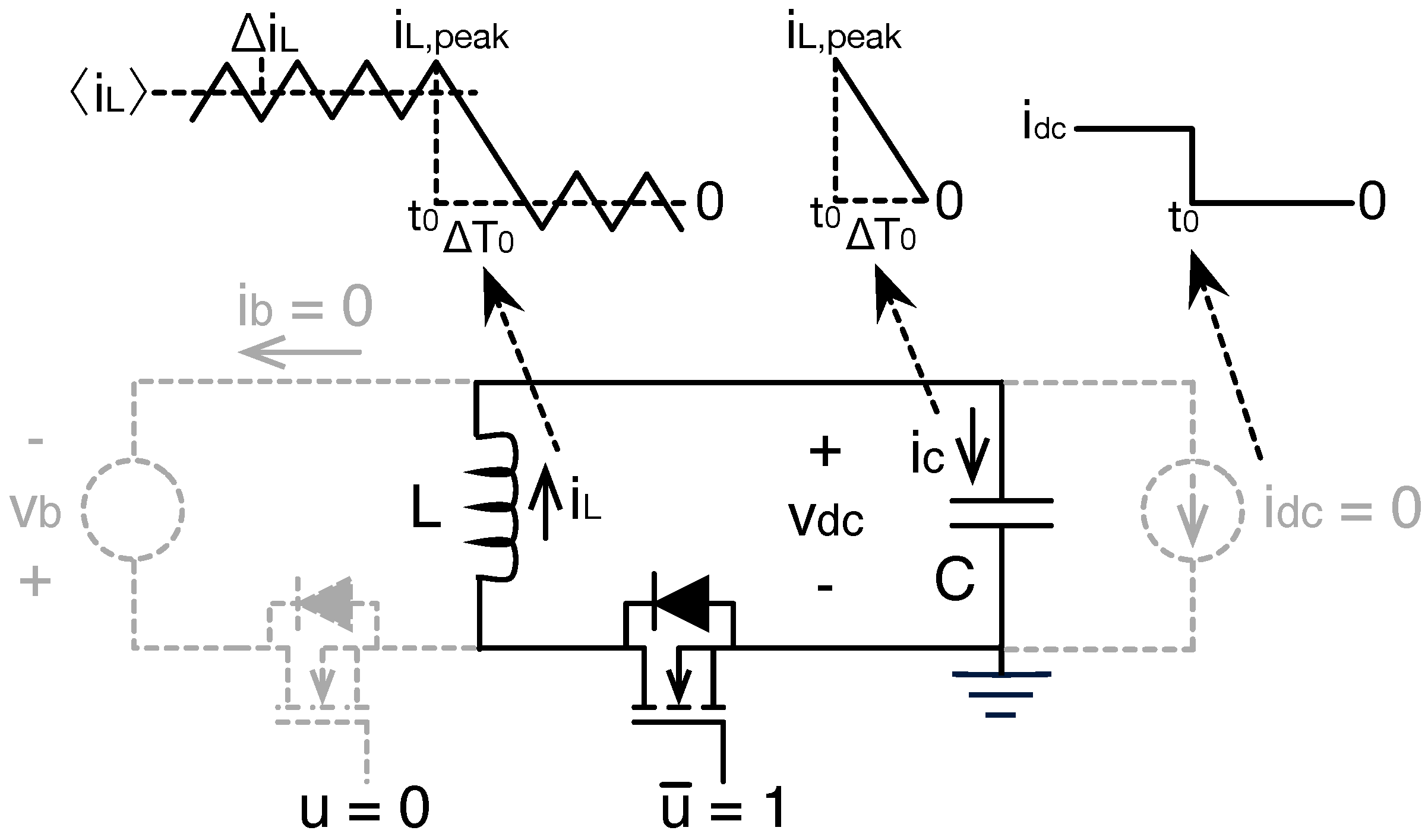
2. Charger-Discharger Circuit and Model
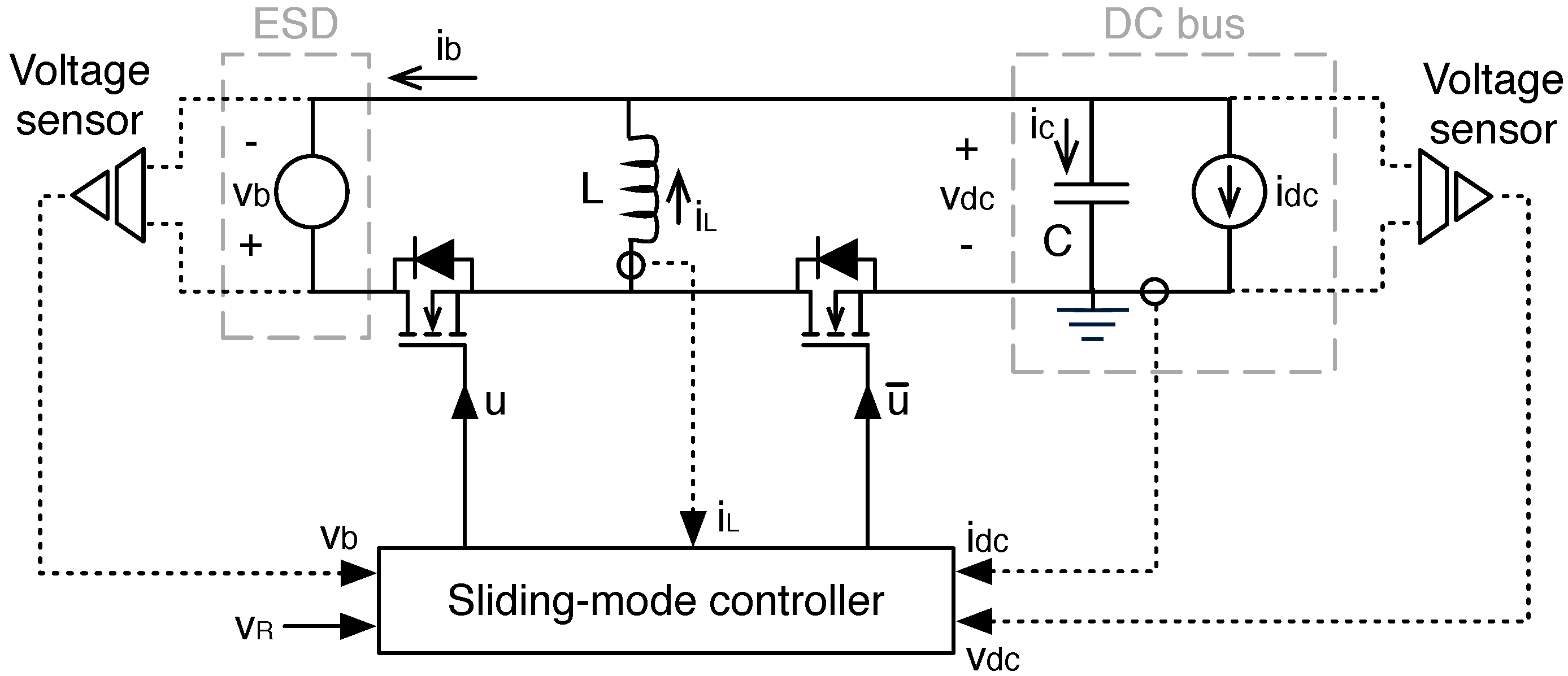
The charger–discharger circuit adopted in this paper is presented in
Figure 1. This charger–discharger is based on a bidirectional Buck–Boost topology [
43]; hence, it is capable of interfacing an ESD and a DC-bus with any voltage relation. In this electrical model, the ESD is represented with a voltage source due to the large capacitance of the ESD [
30], while the DC-bus is represented with both a capacitor
C and a current source. Such a DC-bus representation aggregates into the current source
both the current demand of the loads and the current supply of the energy resources connected to the DC-bus. Hence,
could be either positive (power must be extracted from the ESD) or negative (power must be stored into the ESD) depending on the power balance between loads and energy resources.
The circuital scheme in
Figure 1 defines the physical variables used to design and process the converter controller aimed at regulating the DC-bus voltage: the ESD voltage
, the DC-bus voltage
, the DC-bus current
, the inductor current
and the desired (reference) DC-bus voltage
. The controller generates the control signal
u and the complementary signal
in order to define the states of the MOSFETs (Metal-Oxide-Semiconductor Field-Effect Transistor). In addition, the scheme also defines the current conventions for both the ESD and capacitor currents, i.e.,
and
, respectively.
The switched differential equations for the inductor current
(
1) and capacitor (DC-bus) voltage
(
2) are obtained by using the charge and flux balance principles [
43]. In these expressions,
L and
C are the values of the converter inductance and DC-bus capacitance, respectively:
The small-ripple approximation [
43] considers averaging the DC/DC converter signals during each switching period
to remove the switching ripple. The duty cycle
d of the charger–discharger, given in Equation (
3), is obtained by applying the small-ripple approximation to the MOSFET signal
u. Similarly, the averaged inductor current
and capacitor voltage
differential equations are given in Equations (
4) and (
5), respectively:
The voltage conversion ratio
and the averaged capacitor current
of the converter are obtained from Equations (
4) and (
5) as follows:
Finally, from Equation (
6), it is possible to define
, which makes evident that the duty cycle only depends on the averaged values of the capacitor and ESD voltages; hence, it is independent from the sign of both inductor and DC-bus currents.
3. Sliding-Mode Controller
The regulation of the DC-bus voltage must be ensured in any operation condition, i.e., charging the ESD, discharging the ESD or in stand-by mode (null ESD current). This paper proposes a nonlinear controller based on the sliding-mode theory to achieve that goal.
The sliding-mode controller (SMC) must minimize the error between the DC-bus voltage
and the desired reference
. Moreover, from the circuit in
Figure 1, it is observed that the main perturbation for the DC-bus voltage corresponds to the variations in the DC-bus current
. Those perturbations, as reported in Equation (2), can be rapidly compensated by acting on the inductor current
to avoid large deviations of the DC-bus voltage from
. Therefore, the sliding surface governing the closed-loop regime must include the voltage error, the DC-bus current and the inductor current. The switching function
and sliding surface
proposed to implement the SMC are reported in Equations (
8) and (
9), respectively, in which the parameters
and
must be calculated to provide the desired dynamic response:
Moreover, the analysis of the SMC requires the calculation of the switching function derivative, which is given in Equation (
10). It must be noted that Expression (
10) considers a constant reference value
, i.e.,
, which is a correct assumption since the DC-bus voltage of a microgrid must be constant [
30]:
Finally, the explicit derivative of the switching function is calculated by replacing Equations (
1) and (
2) into Equation (
10) as follows:
To ensure the existence of the sliding-mode, thus the system global stability, three conditions must be fulfilled [
44]: transversality, reachability and equivalent control. However, Sira-Ramirez demonstrated in [
45] that equivalent control and reachability conditions are equivalent. Therefore, the following subsections analyze the transversality and reachability conditions of the proposed SMC.
3.1. Transversality Condition
The transversality condition evaluates the capacity of the SMC to modify the system trajectory. The mathematical representation of the transversality test is given in Expression (
12) [
44], which means that the control signal
u must be present into the switching function derivative (
11). The fulfillment of condition (
12) ensures the controller is able to modify the behavior of the switching function
, which makes it possible to drive
to operate within the sliding surface
. Otherwise, if condition (
12) is not fulfilled, the switching function is not controllable with
u and the closed-loop system will not be stable:
Replacing Equation (
11) into Expression (
12) leads to Equation (
13), which ensures that an SMC implemented with Equations (
8) and (
9) fulfills the transversality condition. It must be highlighted that conditions
and
are required to ensure the transversality condition (
13). Those assumptions are correct since both
and
parameters must be different from zero to enable the inclusion of the voltage error and inductor current into the switching function:
The next step to evaluate the stability of the SMC is to analyze the reachability conditions. Those conditions evaluate the ability of the switching function
to reach the surface
: when
the switching function derivative must be positive to reach
, i.e., condition (
14); when
the switching function derivative must be negative to reach
, i.e., condition (
15):
However, the analyses of Expressions (
14) and (
15) depend on the sign of the transversality value [
44]. A positive sign of Equation (
13) implies a positive sign of
for
and a negative sign of
for
. Instead, a negative sign of Equation (
13) implies a positive sign of
for
and a negative sign of
for
. Those practical reachability conditions are summarized in Expressions (
16) and (
17):
Therefore, the selection of the appropriate reachability conditions, between Expressions (
16) and (
17), requires the analysis of the transversality value (
13). Nevertheless, the sign of Equation (
13) depends on the signs of
and
; hence, those parameters are investigated in the following subsection using the equivalent dynamics concept.
3.2. Equivalent Dynamics and Parameters Design
The equivalent dynamics concept analyze the effect of the SMC in the closed-loop behavior [
44]. This analysis is performed by assuming stable the closed-loop system, which is mathematically represented by
. Thus, the system (the switching function
) is considered operating into the desired sliding surface
(
9).
Replacing the switching function (
8) into the sliding surface (
9) gives Equation (
18), which enables calculating the closed-loop inductor current given in Equation (
19):
Averaging Equation (
19) within the switching period, using the small ripple approximation [
43], gives Equation (
20). Then, replacing Expression (
20) into the averaged differential equation of the DC-bus voltage (
5) leads to Equation (
21), which describes the dynamic behavior of the averaged DC-bus voltage under the action of the SMC:
It must be noted that the difference between and the DC-bus voltage corresponds to the switching ripple, hence a stable also ensures a stable .
Expression (
21) considers the action of the SMC; hence, the control signal
u is not present. Instead, this expression includes the converter duty cycle, which must be almost constant when the controller is operating properly, i.e., the DC-bus voltage is regulated near the desired value. Under the light of such a realistic assumption, the dynamic behavior of Equation (
21) is expressed in frequency domain using Laplace transformation as given in Equation (
22):
From Expression (
22), the following conditions are identified:
and must exhibit the same sign to impose a stable equivalent pole at , which guarantees a stable closed-loop behavior.
In steady-state, the value of is transferred to (and ) with a gain equal to 1, i.e., without error. Similarly, in steady-state, the value of is transferred to both and with a gain equal to .
The last condition imposes a steady-state error to the DC-bus voltage when the DC-bus current is different from zero. Therefore, the adaptive value of
, given in Equation (
23), is calculated from Expression (
22), which ensures a rejection of the error introduced by the DC-bus current
. Moreover, since
is positive, it is concluded that
must be also positive to provide a stable closed-loop behavior:
Taking into account the adaptive law for
, imposed in Equation (
23), the new closed-loop dynamic of the DC-bus voltage is:
The closed-loop behavior given in Equation (
24) corresponds to a first-order system with a time constant
. Therefore, the DC-bus voltage reaches the desired value
after a settling time
for the 2% criterion [
30]. With that information, the value of
given in Equation (
25) is calculated to impose the desired settling time
to the DC-bus voltage:
Finally, since both
and
parameters have been calculated in Equations (
23) and (
25), respectively, the design of the proposed SMC is complete. However, the reachability conditions must be analyzed to ensure the sliding function reaches the sliding surface. Those conditions are evaluated in the following subsection.
3.3. Reachability Conditions and Dynamic Restrictions
Taking into account that both
and
have been designed, the sign of the transversality value (
13) must be evaluated to define the correct reachability conditions for the proposed SMC. Moreover, the sign of the transversality value also defines the circuital implementation of the SMC [
44]; thus, the sign of the transversality value must be the same for all the operation conditions; otherwise, a realizable circuit will be difficult to synthesize.
The first step for the sign analysis is to replace the values of
and
, given in Equations (
23) and (
25), into the transversality value (
13):
Then, such an expression must be analyzed for each operation condition as follows:
Stand-by mode: the charger–discharger is not exchanging power between the ESD and the DC-bus; hence, the DC-bus and inductor currents are zero, i.e.,
and
. This imposes a positive transversality value because both
and
L are positive:
Therefore, the transversality value must be positive in the other two operation conditions.
Charge mode: the ESD is charged using power delivered by the DC-bus; hence, the DC-bus and inductor currents are negative, i.e.,
and
. This imposes a positive transversality value because
,
L and
are positive:
Discharge mode: the ESD is discharged to deliver power into the DC-bus, hence the DC-bus and inductor currents are positive, i.e.,
and
. In this case, the restriction given in Expression (
29) must be fulfilled to ensure a positive transversality sign:
The most restrictive condition occurs at the maximum value of the inductor current
, which is calculated from the steady-state relations (
6) and (
7) as
. Therefore, the most restrictive condition for the closed-loop settling time
that ensures a positive transversality value is:
Introducing restriction (
30) in the designing of
(
25) ensures a positive transversality value. Therefore, the reachability conditions given in Expression (
16) hold for the SMC proposed in this paper. The first reachability condition is the result of replacing Equation (
11) into the first inequality of Expression (
16):
Replacing
(
23) and
(
25) into Expression (
31), the following dynamic restriction is obtained:
Similarly, the second reachability condition is the result of replacing Equation (
11) into the second inequality of Expression (
16):
Replacing
,
,
and
d into Expression (
33) imposes the following dynamic restriction:
Fulfilling the dynamic restrictions given in Expressions (
32) and (
34) ensure that both reachability conditions (
31) and (
33) are also fulfilled. Therefore, the maximum and minimum derivatives of the DC-bus current must be constrained by Expressions (
32) and (
34), respectively. It must be highlighted that he selected
value must be tested into Expressions (
32) and (
34) using the expected derivatives appearing in the DC-bus current, which can be calculated from the dynamic behavior of the energy sources and loads connected to the microgrid.
In addition, the dynamic restrictions (
32) and (
34), simultaneously with the relation between
,
and
C given in Equation (
25), are used to design the charger–discharger: the values of
L and
C are calculated to provide the desired settling-time and to ensure the stability of the DC-bus voltage. Such a design process for
L and
C will be described in
Section 5.
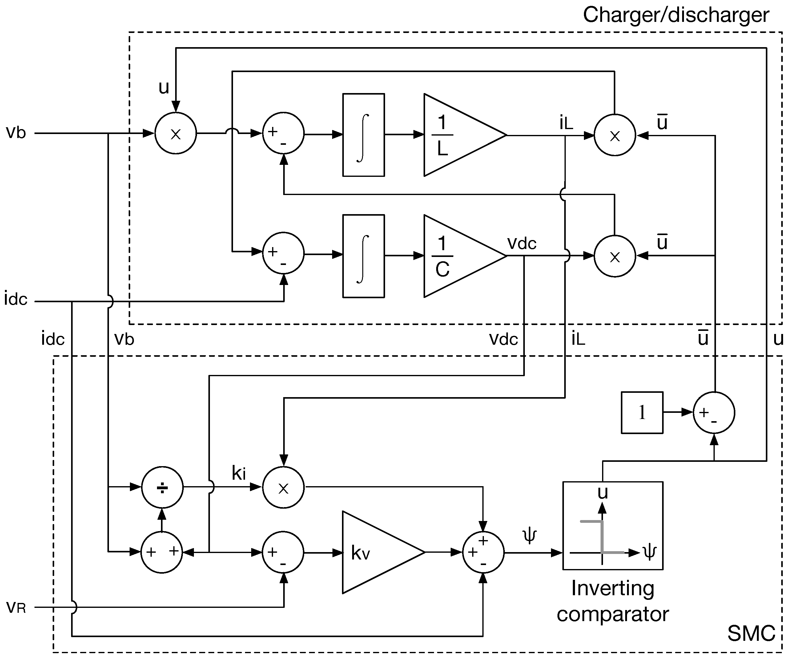
4. Controller Implementation
The proposed SMC requires measuring the inductor current
, the ESD voltage
, the DC-bus voltage
and current
. Moreover, the SMC produces the activation signals
u and
for both MOSFETs of the charger–discharger (see
Figure 1).
The block diagram of the state-space representation for both the charger–discharger and the SMC is presented in
Figure 2. In such a block diagram, the switching function
is synthesized as follows:
parameter is dynamically calculated using the values of the ESD and DC-bus voltages as given in Equation (
23), while parameter
is calculated off-line using Equation (
25) to impose the desired settling time
. Then, the value of
is calculated as reported in Equation (
8).
The switching law for the MOSFETs is defined by the reachability conditions: from Expression (
31), it is recognized that a negative value of
requires
to ensure
; similarly, from Expression (
33), it is recognized that a positive value of
requires
to ensure
. That switching law, summarized in Expression (
35), corresponds to an inverting comparator, which is also depicted in the block diagram of
Figure 2. Finally, the generation of
from
u is also presented in
Figure 2:
Unfortunately, the theoretical switching law given in Expression (
35) imposes an infinite switching frequency [
44], which is impossible to achieve using commercial MOSFETs. This implementation problem is addressed by introducing an hysteresis around the desired condition
to constrain the switching frequency into a practical range [
44]. The practical switching law is given in Expression (
36), which introduces an hysteresis
H into the sliding surface:
The following subsections describe the switching circuit used to implement the practical switching law, the design of the hysteresis band H, the switching frequency and the switching ripples imposed to the charger–discharger.
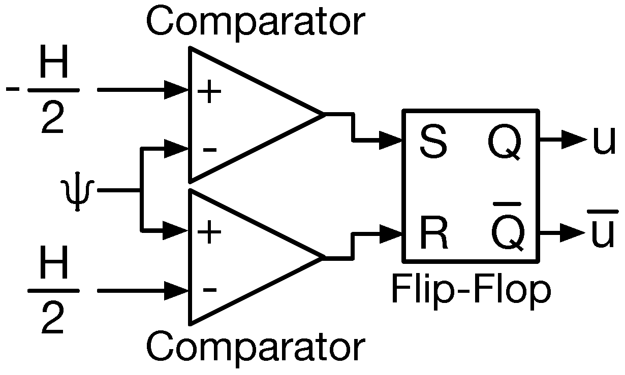
4.1. Switching Circuit
The implementation of the practical switching law (
36) is perfomed with the following conditions:
The corresponding circuit is implemented using two classical comparators to detect conditions (
37) and (
38) as reported in
Figure 3. Those comparators act on the SET and RESET signals of a S-R Flop-Flop to generate both
u and
waveforms: the comparator implementing Expression (
37) turns ON (SET)
u, while the comparator implementing Expression (
38) turns OFF (RESET)
u. Finally, the signals
u and
act on the drivers of the charger–discharger MOSFETs.
4.2. Switching Ripples
The switched operation of the MOSFETs produce ripples in both the inductor current (
) and the DC-bus voltage (
) around their averaged values
and
, respectively [
43]:
The switched differential Equations (
1) and (
2) impose the following derivatives to
and
for
:
The standard notation [
43] defines
during the time interval
. Then, the current ripple waveform of the inductor during
, around
, is given in Equation (
42). In that expression,
is the magnitude of the peak current ripple reported in Equation (
43). Therefore, the maximum value of
is
and the minimum value of
is
:
It is noted that
increases for
in any operation condition. However, the voltage ripple waveform in the DC-bus
decreases in
discharge mode (
), increases in
charge mode (
) and it is equal to zero in
stand-by mode (
) as reported in Expression (
41). The definition of
is given by Expression (
44), where
is the magnitude of the peak voltage ripple reported in Equation (
45):
From the previous expressions, it is concluded that the maximum value of is and the minimum value of is .
Finally, Expressions (
43) and (
45) enable the calculation of the peak ripples of the inductor current and DC-bus voltage depending on the steady-state values of the duty cycle
d, switching period
, ESD voltage
, DC-bus current
,
L and
C parameters. Moreover, those expressions are also used to design
L and
C in agreement with the desired current and voltage ripples for the charger–discharger.
4.3. Switching Frequency
Implementing an SMC with an hysteresis band imposes a variable switching frequency [
44], whose maximum value must be supported by the MOSFETs used to construct the charger–discharger. Therefore, predicting the switching frequency is essential to select the appropriate semiconductor devices.
Assuming a correct operation of the SMC, which is ensured by the transversality and reachability conditions analyzed in
Section 3, the averaged DC-bus voltage is equal to the reference voltage:
. Moreover, since
, the averaged value of the term
in
(
8) is
, which is equal to the averaged value of the capacitor current
given in Equation (
7). Taking into account that the charge balance principle [
43] ensures that
in steady-state, the relations between the ripples and averaged values given in Equations (
39) and (
40) lead to the following steady-state waveform of the switching function
around 0:
To fulfill the hysteresis band, the minimum and maximum values of
are
and
, respectively. Moreover, the peak values of
occur at the peak values of
and
because those waveforms are synchronized by
u as reported in Equations (
1) and (
2).
Then, the peak value of Equation (
46) must be analyzed in the three operation modes of the charger–discharger:
Discharge mode (
):
and
have opposite derivatives as reported in Expression (
41), hence the maximum value of
occurs when
is minimum. This condition leads to the following expression for the peak value of
:
Stand-by mode (
):
as reported in Expression (
44), hence the peak value of
occurs at the peak value of
:
Charge mode (
):
and
have derivatives with the same sign as reported in Equation (
41), hence the maximum value of
occurs when
is maximum. This condition leads to the following expression for the peak value of
:
Replacing the values of
(
25),
(
43) and
(
45) into Equations (
47)–(
49) produce the following expressions for the switching frequency:
From the previous expressions, it is concluded that
charge mode produces higher switching frequencies. Therefore, the hysteresis band
H must be calculated as given in Equation (
53) to ensure a maximum switching frequency
. In that expression,
corresponds to the maximum magnitude of the DC-bus current expected in
charge mode:
Finally, Equation (
53) ensures a switching frequency below
for the three operating modes, hence any commercial MOSFET supporting switching frequencies higher than
will operate correctly under the action of the proposed SMC.
6. Design Example
The following parameters are adopted to illustrate the performance of the proposed solution: an ESD voltage (
) equal to 12 V, a desired DC-bus voltage (
) equal to 24 V, a DC-bus current up to 1 A with maximum derivatives
(
). This speed in the current transients is common in automotive battery test systems, which are used to create the current profiles for life cycle evaluations of batteries, as reported in [
46,
47]. Moreover, to avoid damage in the loads and energy resources, the maximum DC-bus voltage must be limited to 1 V over the nominal value (up to 25 V). Finally, DC-bus voltage must be restored after 2 ms and the switching frequency must be limited to 55 kHz, which enables the use of inexpensive MOSFETs.
This example illustrates the simplicity of the circuit design process by means of four steps: design the inductor of the charger–discharger, design the capacitance of the DC-bus, design the controller parameters and design the hysteresis band of the switching circuit.
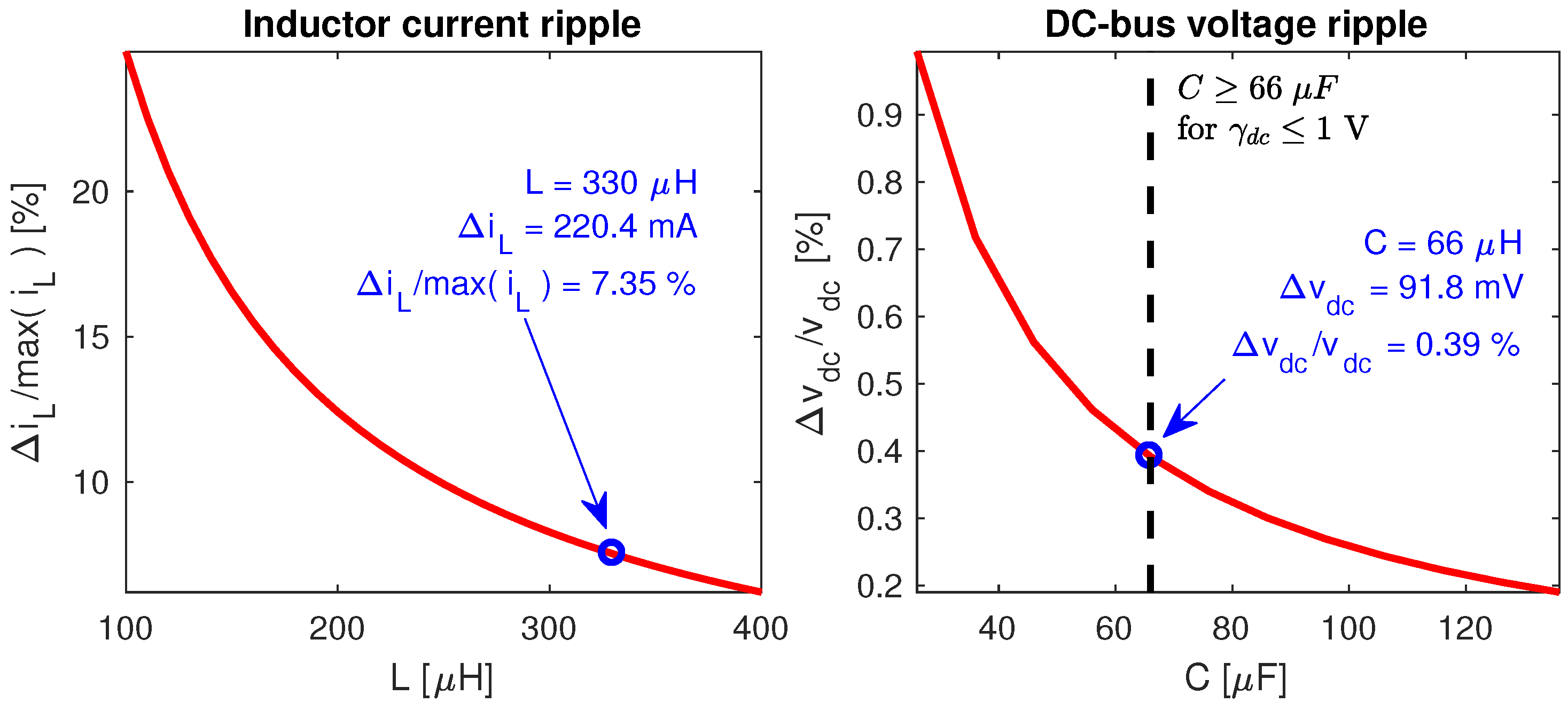
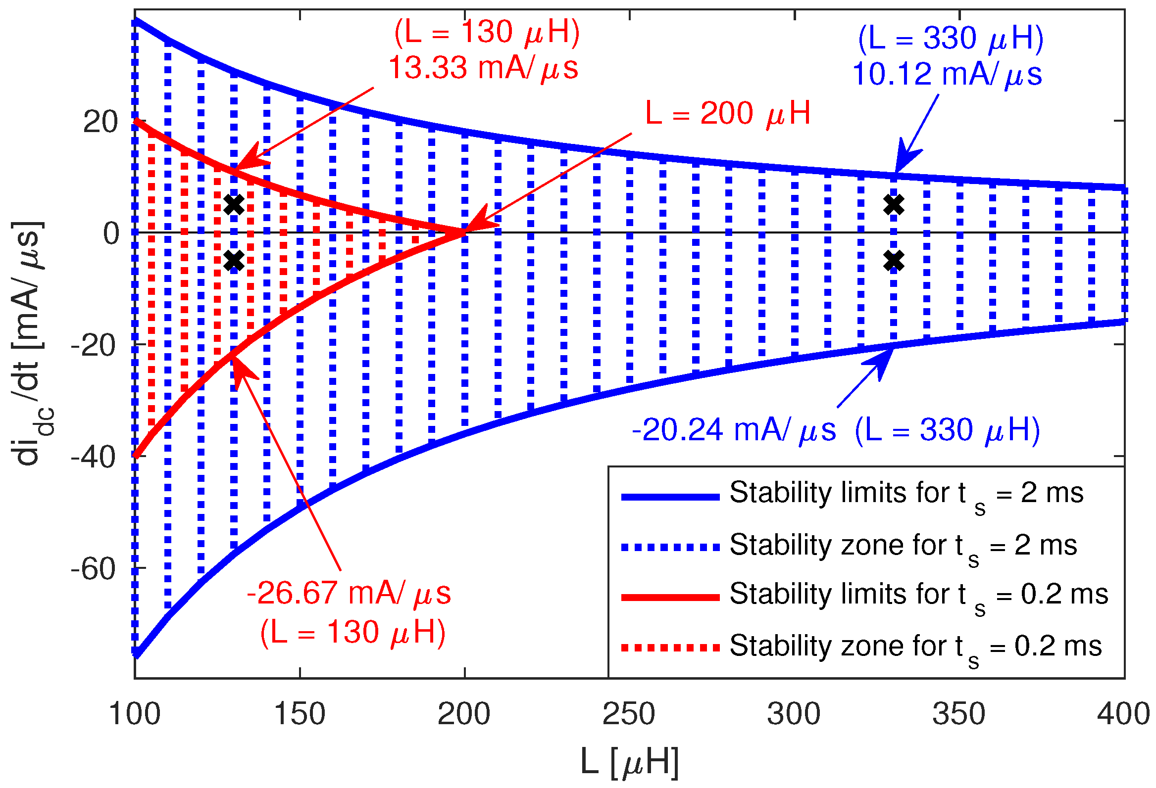
The first step is to construct the inductor design plot presented in
Figure 5 using Expressions (
32) and (
34) for
. From that plot, it is noted that
ensures the dynamic stability for the expected current transient derivative
. However, two additional conditions must be considered: the tolerance of commercially available inductors and the current ripple injected into the ESD. To account for the tolerance, this example considers a factor of two for the current derivative, so that the inductor is selected from
Figure 5 for
, which requires
. A near commercially available inductor value is
, e.g., the inductor 2218-H-RC from Bourns Inc.
Figure 6 makes evident that
provides a stable operation of the circuit for
.
Then, the inductor current ripple is calculated from Equation (
43) for the desired switching frequency;
Figure 10 shows the current ripple produced by different inductor values. It is observed that the commercially available
produces a current ripple of
, which corresponds to the 7.35% of the maximum inductor current
. This current ripple is acceptable in terms of the small-ripple approximation [
43]; hence, the inductor value
is selected for this example. Nevertheless, smaller current ripples are achievable by increasing the inductor but without exceeding the limit imposed by
.
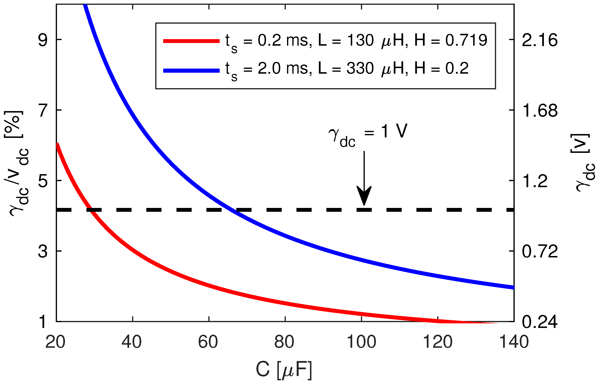
The second step is to design the DC-bus capacitance to fulfill the maximum overvoltage value
. The minimum value of the capacitance
ensuring
is calculated from Equation (
57). This is confirmed in
Figure 8, which shows that any capacitor higher than
will ensure
. Another characteristic to be evaluated is the voltage ripple in the DC-bus, which depends on
C as reported in Equation (
45).
Figure 10 reports the voltage ripples in the DC-bus for multiple values of
C, where the minimum capacitance
produces a voltage ripple of 91.8 mV (
of the nominal DC-bus voltage). This small voltage ripple is acceptable in terms of the small-ripple approximation [
43].
The capacitance tolerance is not mandatory to be considered because the DC-bus design is performed in the worst case. Nevertheless, the capacitor could be increased to introduce a safe margin or to reduce the voltage ripple. For this example, the limit capacitance value
is adopted, whose usefulness was already validated in
Figure 9: it ensures a DC-bus voltage lower than 25 V for current transients with
. In fact,
limits the DC-bus voltage to 25 V even under the occurrence of an unexpected step-like current transient (
), which could be triggered by the simultaneous disconnection of all the loads from the DC-bus. A commercially available solution is the parallel-connection of two capacitors of
, e.g., two MKT1820633065 capacitors from Vishay BC Components.
The third step is to calculate the SMC parameters. The design of
is given in Equation (
23), which provides an automatic adjustment of the SMC to the ESD and DC-bus voltage conditions, as depicted in the implementation of
Figure 2. The calculation of
is given in Equation (
25), which depends on the bus capacitance
and desired settling-time
, resulting in
for this example.
The final step is to design the hysteresis band
H of the switching circuit in
Figure 3 to limit the switching frequency. The value of
H to ensure a maximum switching frequency of 55 kHz is calculated using Expression (
53) obtaining
. This example adopts
to introduce a small safe margin, which imposes a maximum switching frequency of
. Finally, the circuital scheme implemented in PSIM, i.e.,
Figure 4, is configured using those parameters.
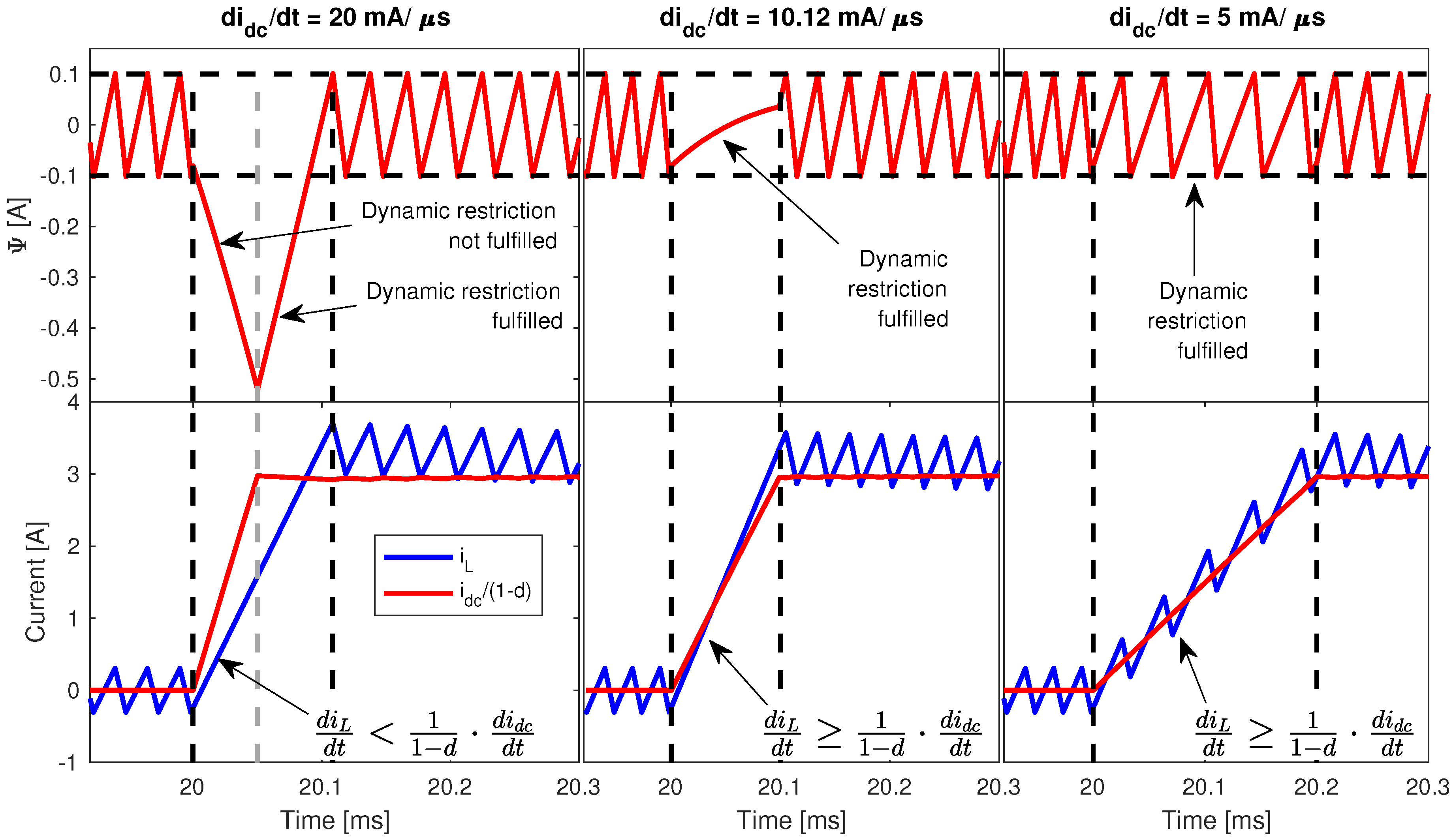
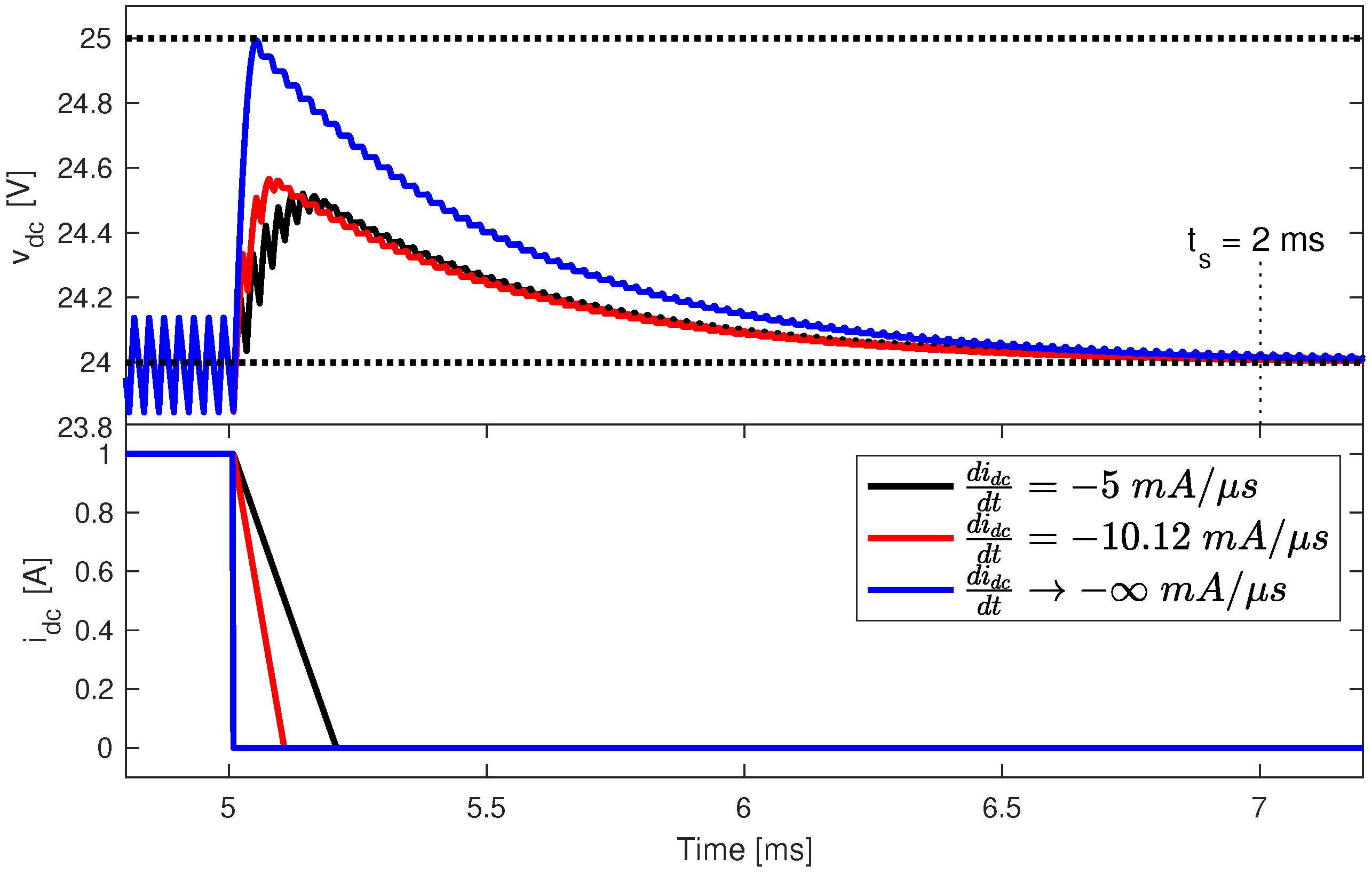
Figure 11 presents the simulation of the PSIM circuit considering current transients in the DC-bus with amplitudes of
and derivatives equal to
.
The simulations at the left in
Figure 11 consider the DC-bus operating at
, which validates the circuit and SMC design: the DC-bus voltage is correctly regulated to
in all of the operating modes (charge, discharge and stand-by); moreover, the DC-bus voltage is constrained to
around
, i.e., the safety restriction
is always fulfilled. This correct behavior is possible because the SMC is always stable. Such a condition is confirmed by the constrained operation of
into the hysteresis band, which also limits the switching frequency. Finally, the DC-bus voltage is restored to
after the designed settling time
in all of the operation conditions.
It must be noted that the design of
is independent from the nominal value of the DC-bus voltage. Moreover,
is continuously adapted by measuring both the DC-bus and ESD voltages. This robustness of the SMC is also validated in the simulations of
Figure 11 by setting
(boost operation),
(Buck–Boost operation) and
(buck operation). The simulations show the same settling time for the bus voltage conditions, which is achieved due to the global stability of the SMC. Furthermore, the overvoltage conditions are always under
because decreasing the DC-bus voltage also decrease
, as reported in Expression (
57). Therefore,
C must be designed for the higher DC-bus voltage.
In conclusion, the proposed SMC and charger–discharger provide a general solution for interfacing an ESD with the DC-bus of a microgrid. This is achieved by the correct regulation of the DC-bus voltage in Boost, Buck and Buck–Boost conditions.
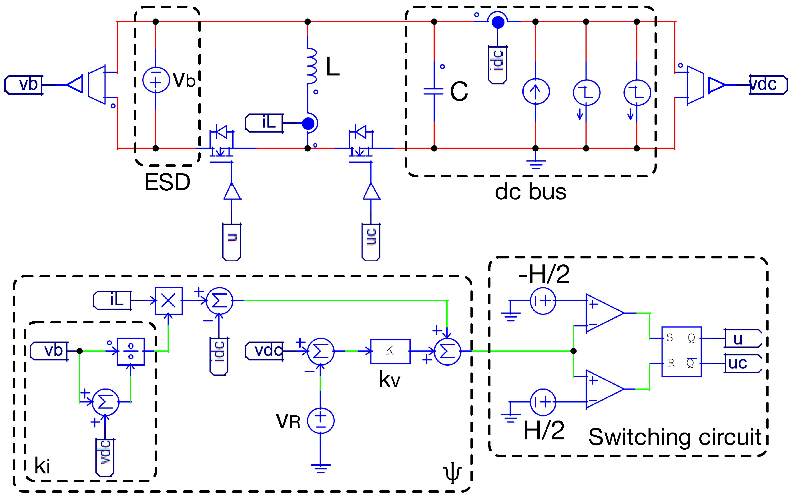
7. Experimental Implementation and Proof-of-Concept
This section presents the experimental validation of the proposed charger–discharger and SMC. A proof-of-concept prototype was developed as reported in
Figure 12.
Figure 12a describes the prototype setup. The selected ESD is a 12V battery from MTEK-SA (Medellín, Colombia), while the DC bus is emulated using a four quadrant electronic source/load BOP 50-20GL from Kepco Inc (Flushing, NY, USA). The proposed surface
is calculated using a F28335 controlCARD from Texas Instruments (Dallas, TX, USA) and converted to an analog voltage with a digital-to-analog converter (DAC) MCP4822. Moreover, the switching circuit of
Figure 3 is implemented with an amplifier, a TS555 integrated circuit, and an A3120 MOSFET driver.
The bidirectional Buck–Boost DC/DC converter is implemented using an 2218-H-RC inductor from Bourns Inc (Altadena, CA, USA) with
, a MKT1813622016 capacitor from Vishay BC (Selb, Germany) with
, and two IRF540N MOSFETs from International Rectifier (El Segundo, CA, USA). Furthermore, the inductor and the DC-bus currents are measured using shunt-resistors
and AD8210 amplifiers. These current and voltage measurements are acquired by the controlCARD using the onboard analog-to-digital converters (ADCs). Finally, the physical setup of the experimental platform is shown in
Figure 12b.
The values of
L and
C are obtained by following the procedure presented in
Section 5 considering the limitations of the experimental setup:
,
,
, and
(
). Moreover,
is obtained from Equation (
53) by defining
.
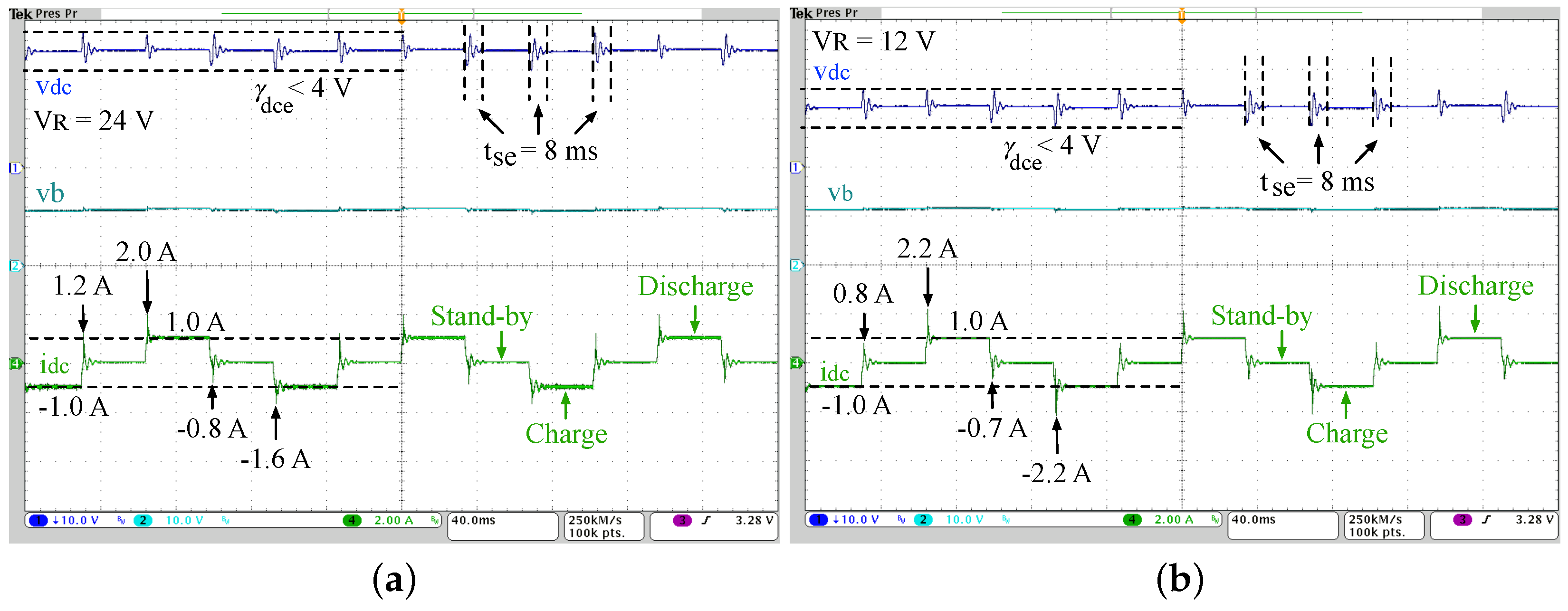
The performance of the proposed solution is evaluated with two experiments, the first one is similar to the simulations presented in
Figure 11, and the second one shows the dynamic response of the system for a large change in the operating point.
In the first experiment, the electronic source/load is programmed to reproduce the
profiles shown in
Figure 11. Three experiments where performed considering the same values of the DC-bus voltage used in
Section 6:
,
, and
, with
. However, the electronic source/load is not able to produce
steps, as shown in
Figure 13, due to its internal dynamic and controllers. The experimental
transients exhibit a second-order behavior, whose maximum overshoots are shown in
Figure 13a,b, and
Figure 13a for
,
, and
, respectively.
In these experiments, the settling-time (
) fulfills the design condition
for the three values of
, as shown in
Figure 13. However, the experimental maximum deviation of
(
) is under
for the three DC-bus voltage values; hence,
is almost
higher than the design condition
. Such a difference between
and
is produced by the
overshoots in the transients, which are between
and
higher than the
value used for the design (
): the fourth transient in
Figure 13a exhibits a peak value of
(
higher); while the second and fourth transients in
Figure 13b and the fourth transient in
Figure 13c exhibit peak values of
(
higher). Therefore, experimenting a
higher
condition for a
higher perturbation in
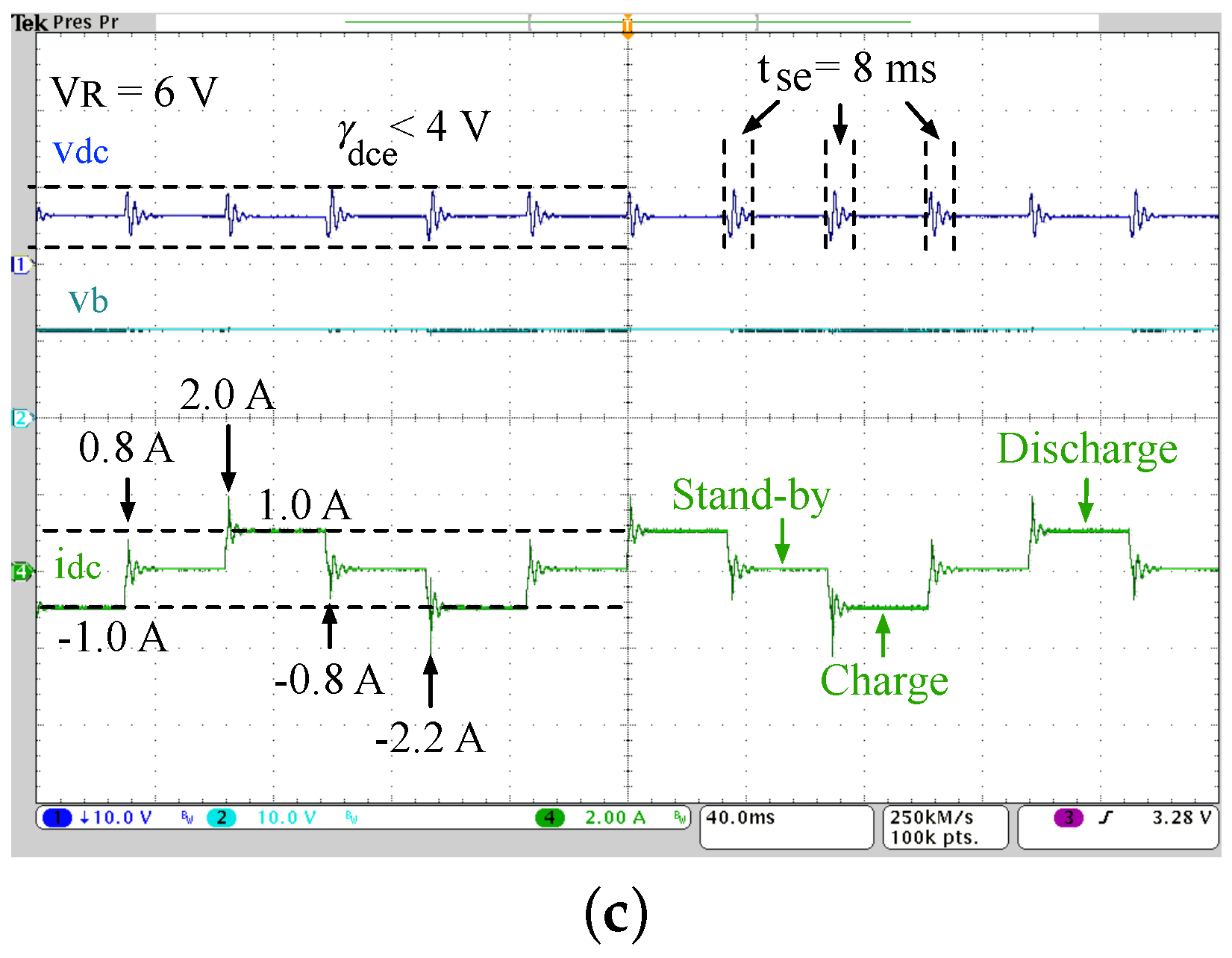
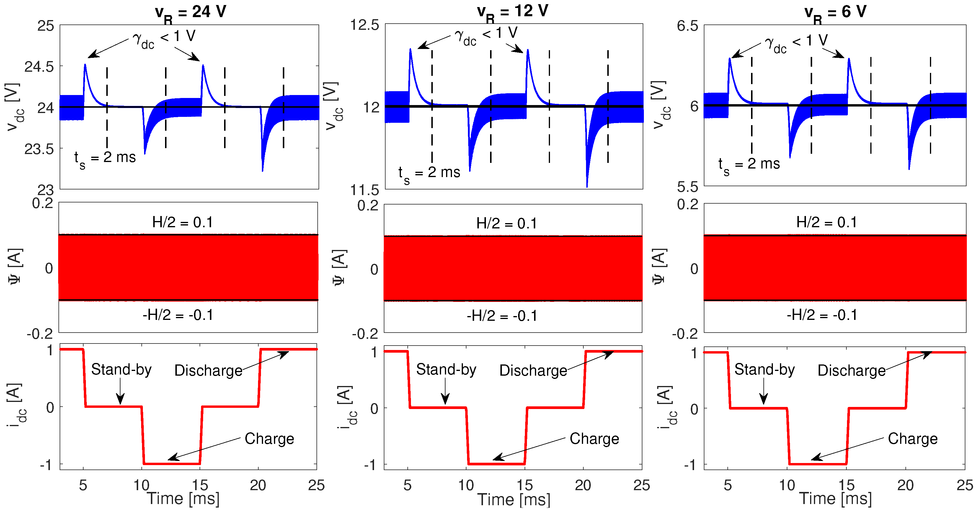
is satisfactory. In conclusion, the results of this first experiment puts into evidence the satisfactory performance of the prototype operating in Boost, Buck–Boost and Buck modes.
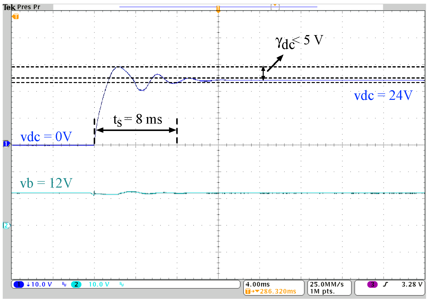
The second experiment shows the dynamic response of the prototype during the startup for a 24 V DC-bus in stand-by mode, i.e., the steady-state value of
is
. The ESD voltage (
) and DC-bus voltage (
) waveforms are presented in
Figure 14, which shows a correct regulation of
at
with a settling-time equal to
. Once again, the experimental settling-time matches the design value (
). In this experiment, the overshoot is close to
, which is caused by the large transient in the capacitor current required to charge the capacitor from
to
. This suggests that, in a commercial application, it is required to include a slow-speed bus charge strategy for the startup process. In conclusion, this second experiment shows the accurate settling time imposed by the proposed solution, even for large changes in the operating point, which makes evident the robustness of the solution.
Finally, those experimental results demonstrate the correctness and usefulness of the proposed SMC and charger–discharger design for DC-bus regulation in microgrids.
8. Conclusions
A system formed by an ESD, a charger–discharger Buck–Boost converter and a DC-bus capacitor has been designed and analyzed. The system includes a sliding-mode controller designed to regulate the DC-bus voltage in both DC and hybrid MGs. On one hand, the use of a Buck–Boost converter allows the connection of an ESD with voltage lower, equal to or higher than the DC-bus voltage, which simplifies the use of commercial ESD systems in MG applications. On the other hand, the SMC provides a robust solution to regulate the DC-bus voltage, which ensures the system stability in the entire operation range of the charger–discharger. Moreover, detailed design and implementation methods for both the SMC and the charger–discharger parameters have been presented.
The SMC and the charger–discharger were designed to fulfill a desired settling time (), a maximum DC-bus voltage () deviation from the reference (), and a maximum switching frequency (). Such design requirements are fulfilled considering a maximum DC-bus current magnitude () and derivative () for a particular MG application. Simulation and experimental results verify the fulfillment of the design requirements for different perturbations in the DC-bus current, which demonstrates the correct operation of the system in the three operation modes: charging, discharging and stand-by.
Therefore, this single device allows for connecting commercial ESDs to DC-buses with a wide range of voltages. Such a characteristic is ideal for developing commercial ESD management systems. Moreover, the robust nonlinear control strategy can be easily implemented in inexpensive control cards, e.g., the F28335 controlCARD from Texas Instruments used in this paper.
The main disadvantage of the proposed solution is the unavoidable voltage deviation caused by the Buck–Boost topology after a current transient occurs, even if the correct design of the capacitance constrains the overvoltage condition to safe limits. This overvoltage can be further reduced by adopting a step-up/down DC/DC converter with a second-order filter at the output, e.g., Cuk, Sepic or Zeta converters. However, the complexity of those fourth-order converters require new sliding-surfaces, which is an interesting topic for improving the step-up/down charger–discharger proposed in this paper. Moreover, in the start-up process, the DC-bus must be charged to the nominal voltage without decreasing the state-of-charge of the ESD. Therefore, a start-up routine must be designed to the charge of the DC-bus from the main power sources of the microgrid. Another interesting topic to explore is the use of three-port converters to regulate the DC-bus voltage of an MG. These converters have the possibility to connect an ESD and a DC power source (like a PV generator) with a single converter, which could help to reduce the number and depth of the ESD charging/discharging cycles.
Finally, the proposed design process assumes the current transients’ derivatives occurring in the DC-bus are known; however, such information is not commonly reported for the commercial devices that can be connected to a DC-bus (e.g., refrigerators, fans, TVs, computers, light bulbs, etc.), and thus a previous load analysis is required.

 ,
, 