Abstract
In this work, kesterite-type Cu2ZnGeSxSe4-x absorbers were prepared by a two-step process for use in thin-film solar cells. Their high band gap makes them an interesting candidate as top cells in multijunction solar cells. However, an exact tuning of the band gap is essential. Therefore, for the first time, the [S]/([S] + [Se]) ratio was controlled via addition of a variable amount of GeS during the annealing step, which allowed precise control of the band gap between 1.5 and 1.7 eV. The changes in morphology and crystallinity of the absorber are discussed in detail. An additional focus was directed toward the parameters of the resulting solar cells. Although the efficiency declined as the [S]/([S] + [Se]) ratio increases, the open-circuit voltage was considerably increased.
1. Introduction
In recent years, the rather new kesterite-type Cu2ZnGeSxSe4-x (CZGSSe) has gained attention as a high band gap absorber material for thin-film solar cells [1,2,3,4,5,6]. Its similarity to the extensively studied Cu2ZnSnSxSe4-x (CZTSSe) offers potential for fast progress in the improvement of material properties and solar cell efficiency, with a record value of 6.0% so far [3]. However, the band gaps in previous publications are in a range between 1.4 eV [4] and 1.5 eV [5] and are therefore still too low for application as top cells in multijunction solar cells.
If one wants to increase the band gap of CZGSSe, one possibility would be to completely or partially substitute the cations. By exchanging Si for Ge, the band gap could be increased to 2.4 eV for Cu2ZnSiSe4 [7]. Alternatively, Cu could be replaced by Ag, which is known to increase the band gap of CZTSe absorbers by more than 0.3 eV [8]. Additionally, Zn could be substituted by Ba, which allows band gaps of 1.85 eV for Cu2BaSnSe4 [9] and 2.05 eV for Cu2BaSnS4 [10]. Besides including other elements, changing the cation composition can also work since decreasing the Cu content is known to increase the band gap for Cu2ZnSnSxSe4-x [11]. However, the most straightforward way to increase the band gap of a kesterite-type absorber is to increase the [S]/([S] + [Se]) ratio, which gives access to band gaps of up to 2.0 eV [12] for Cu2ZnGeS4 (CZGS) and therefore meets the typical band gap requirements of top cells in multijunction solar cells.
In the present study, additional sulfur incorporation into solution-processed CZGSSe layers was achieved by supplying Se and various amounts of GeS during the high-temperature annealing step. With the amount of GeS, the [S]/([S] + [Se]) ratio of the absorber layer can be tuned between 27 and 50%, which gives access to band gaps between 1.5 and 1.7 eV. Although the efficiency declines as the band gap increases, the open-circuit voltage, which is considered to be the main limiting parameter for the performance of solar cells with kesterite-type absorbers, can be considerably increased to a maximum of 699 mV. Detailed absorber properties and solar cell parameters are discussed and compared with values from previous literature.
2. Results
The [S]/([S] + [Se]) ratios of the absorbers that were annealed in the presence of different amounts of GeS have been determined from the shift of the 112-reflection in the X-ray diffractograms (XRD) according to Vegard’s Law [13]. The XRD spectra are displayed in Figure 1a with a detailed view of the 112-reflection in Figure 1b. The reflections were identified according to the reference JCPDS 052-0867. Since the reference card is for Cu2ZnGeSe4 (CZGSe), all reflections are shifted to higher diffraction angles. In the complete spectrum, the 112-reflection at 28.04 is the strongest kesterite reflection. Additional reflections can be seen at 17.99 (101), 31.97 (MoSxSe2-x), 40.47 (Mo), 46.31 (220), 46.69 (204), 55.03 (312), and 56.26 (MoSxSe2-x, partly overlapping with the 312 reflection), which means that there is no indication for secondary phases besides the commonly observed MoSxSe2-x. Note that the intensity of the MoSxSe2-x-reflections decreases as the amount of GeS increases, which suggests a lower MoSxSe2-x thickness.
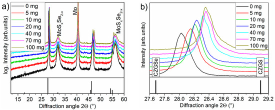
Figure 1.
XRD-spectra of CZGSSe absorbers that were annealed in the presence of different amounts of GeS (a) with a detailed view of the 112-reflection (b). The reference card for CZGSe (JCPDS 052-0867) has been added to Figure 1a to allow for an identification of the reflections. In Figure 1b, the reference for CZGS (JCPDS 074-8334) has also been added to illustrate the shift from CZGSe to CZGS.
A summary of all 112 reflection positions and the calculated [S]/([S] + [Se]) ratios are displayed in Table 1. Note that, for the calculation of the [S]/([S] + [Se]) ratio, the position of the 112-reflection has been corrected by the shift of the 110-reflection of Mo that should occur at 40.499 (JCPDS 01-089-5156). Even before any GeS was used during annealing, the [S]/([S] + [Se]) ratio was already 0.27, as the precursor contains sulfur, which is only partly replaced by Se during the annealing step. As the amount of GeS increased, the [S]/([S] + [Se]) ratio was gradually enlarged until saturation occurred at approximately 0.5 for a GeS amount of 70 mg, and no more S could be incorporated by further increasing the amount of GeS to 100 mg.

Table 1.
Position of the 112-reflection and [S]/([S] + [Se]) ratios for CZGSSe absorbers annealed in the presence of different amounts of GeS. Note that the positions of the 112-reflections were corrected by the shift of the 110-reflection of Mo for the calculation.
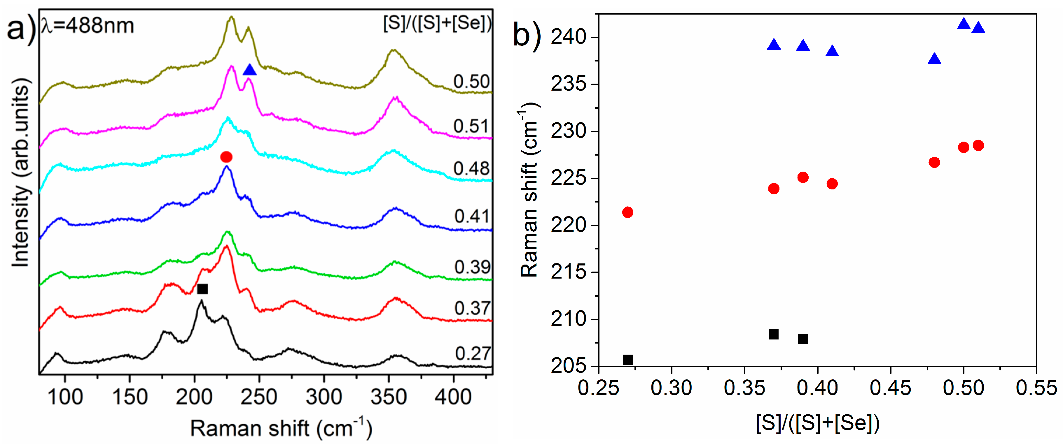
To gain additional information about crystallinity and phase composition, multiwavelength Raman microscopy was performed on all samples. The results with an excitation wavelength of 488 nm are shown in Figure 2. For the sample without added GeS, kesterite modes were detected at 94, 180 (which consists of two modes [14]), 206, 274, and 357 cm−1, which are all in agreement with previous Raman studies [14,15,16]. However, in comparison to the cited publications, all modes were slightly shifted due to the mixed sulfoselenide composition.
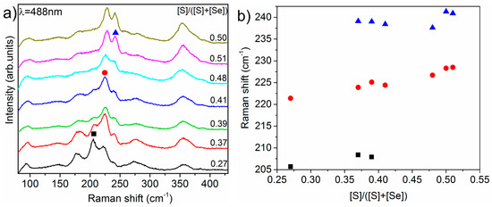
Figure 2.
(a) Raman spectra of CZGSSe absorbers that were annealed in the presence of different amounts of GeS as indicated, measured with an excitation wavelength of 488 nm. (b) Raman shifts of the sulfoselenide CZGSSe modes.
Additionally, two more modes were observed: a very weak mode at 147 cm−1 that could not be attributed to the kesterite or any secondary phase and a sharper mode at 221 cm−1 that was previously reported for CZGSSe [17]. The latter one is especially interesting since it became the most intense mode when the [S]/([S] + [Se]) ratio was increased to 0.37. When the amount of S was further increased, it shifted to higher wavenumbers up to 228 cm−1 for the sample annealed with 100 mg of GeS ([S]/([S] + [Se] = 0.51, displayed in Figure 2b). Simultaneously, the CZGSe-like mode at 206 cm−1, which was the most intense mode for the sample without added GeS, lost intensity and finally vanished. Instead, a second CZGSSe-like mode at 241 cm−1 gained in intensity, which was present only as a small shoulder in the spectrum of the sample annealed without GeS. Its position is close to a mode reported for GeS [18]. However, since the absorber composition was slightly Ge-poor, it is more likely that it was one more sulfoselenide mode related to vibrations of both S and Se anions. A similar behavior has been reported for CZTSSe by Dimitrievska et al., who observed three additional sulfoselenide modes in addition to the CZTS-like and CZTSe-like modes [19].
Additional measurements were performed with excitation wavelengths of 457 nm (resonant for ZnSe) and 325 nm (resonant for ZnS, both not shown) without revealing additional structures, so the presence of these secondary phases can be excluded. However, note that Raman spectroscopy is a surface sensitive technique; therefore, the conclusions drawn here do not necessarily account for the deep bulk of the absorbers.
In addition to the structural characterization, the morphology of the prepared CZGSSe layers was examined by scanning electron microscopy (SEM) measurements of the cross section, as displayed in Figure 3. All absorber layers exhibited a two-layer morphology with a large-grain layer on top and a small-grain layer underneath. For the morphology of the absorber itself, the [S]/([S] + [Se]) ratio does not make a difference since there is no trend for a change in the grain size or the ratio of a large-grain to small-grain layer. However, the thickness of the MoSxSe2-x layer constantly declined from 1000 to 550 nm as the [S]/([S] + [Se]) ratio increased. This is in good agreement with previously described XRD measurements, where the intensity of the 110 reflection of MoSxSe2-x decreased with the amount of GeS, while the reflection position was shifted to higher diffraction angles (see Figure S1). The most likely explanation for the decreasing thickness is that, as S-inclusion increases, the MoSxSe2-x forms a barrier for the diffusion of bigger Se ions, thereby inhibiting further growth of the layer.
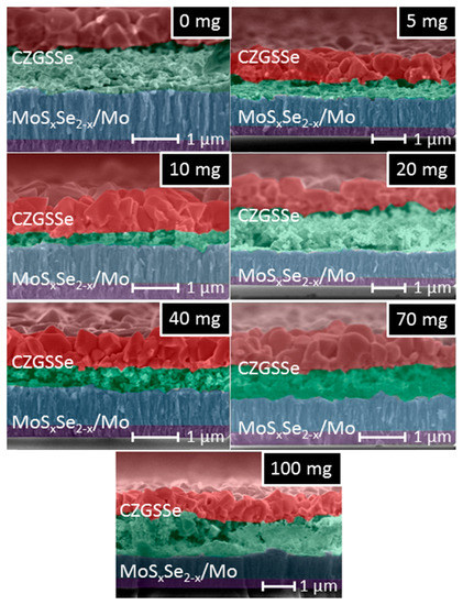
Figure 3.
Cross-section SEM measurements of CZGSSe absorbers that were annealed in the presence of different amounts of GeS as indicated. For a better identification, the layers are colored with red for the large-grain CZGSSe, green for the small-grain CZGSSe, blue for MoSxSe2-x, and purple for Mo.
If one estimates the [S]/([S] + [Se]) ratio of MoSxSe2-x in the same way as CZGSSe (Figure S2), a stronger S-inclusion is found in the MoSxSe2-x layer than in the absorber.
A similar trend has been observed by X-ray photoelectron spectroscopy for CuInxGa1-xSySe2-y. There, the decreasing thickness of the MoSxSe2-x layer and the stronger S-inclusion in comparison to the absorber were attributed to the higher formation energy (and therefore a preferred formation) of MoS2 in comparison to MoSe2 [20].
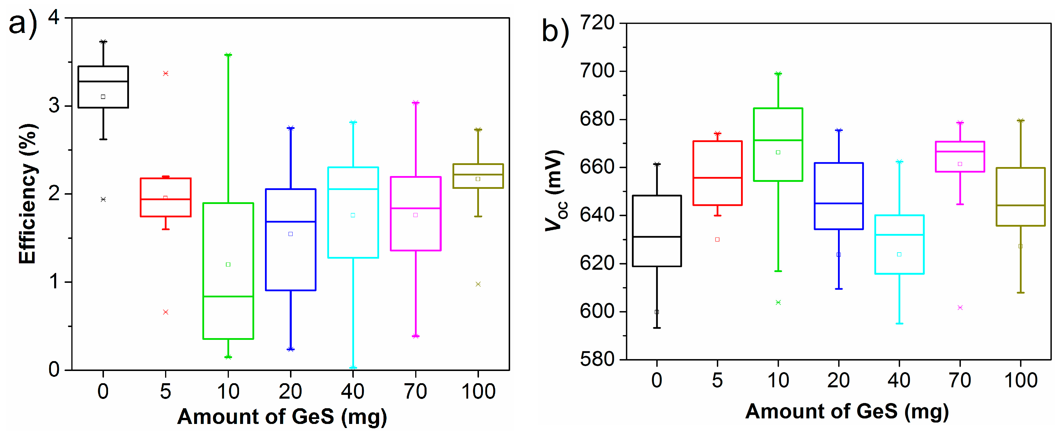
After processing the absorbers to solar cells, the current–voltage (J-V) characteristics were measured. The efficiency η and open-circuit voltage VOC are displayed as box plots in Figure 4, and the JV-characteristics can be found in the supplementary materials. For the efficiency (Figure 4a), the highest average value of 3.1% was achieved without adding GeS. When the amount of GeS is increased, the efficiencies strictly decline, reaching a minimum of only 1.2% for 10 mg of GeS (where also the strongest deviations occur). When more GeS is used, the efficiencies slightly increase, up to 2.2% for 100 mg of GeS. A similar trend was observed for the fill factor and short-circuit current density (Supplementary Materials) and may be related to the generally increased series resistance when GeS was added during the selenization.

Figure 4.
Box plots of efficiency (a) and open-circuit voltage (b) of solar cells fabricated from CZGSSe absorbers that were annealed in the presence of different amounts of GeS.
On the contrary, the average VOC increased with added GeS and reached the highest average value of 666 mV for 10 mg (with a maximum value of 699 mV; Figure 4b). However, for a larger amount of GeS, the VOC declined despite the increased band gap. There can be two reasons for this behavior: either (i) the recombination in the bulk increases with a higher [S]/([S] + [Se]) ratio or (ii) the band alignment with the CdS buffer becomes worse, increasing detrimental interface recombination. The latter is very likely, since CdS has been reported to have a decent spike-like band alignment with CZTSSe [21,22], and the conduction band minimum of CZGSe is about 0.5 eV higher than the one from CZTSe [7]. However, an increased bulk recombination with a higher [S]/([S] + [Se]) ratio cannot be excluded.
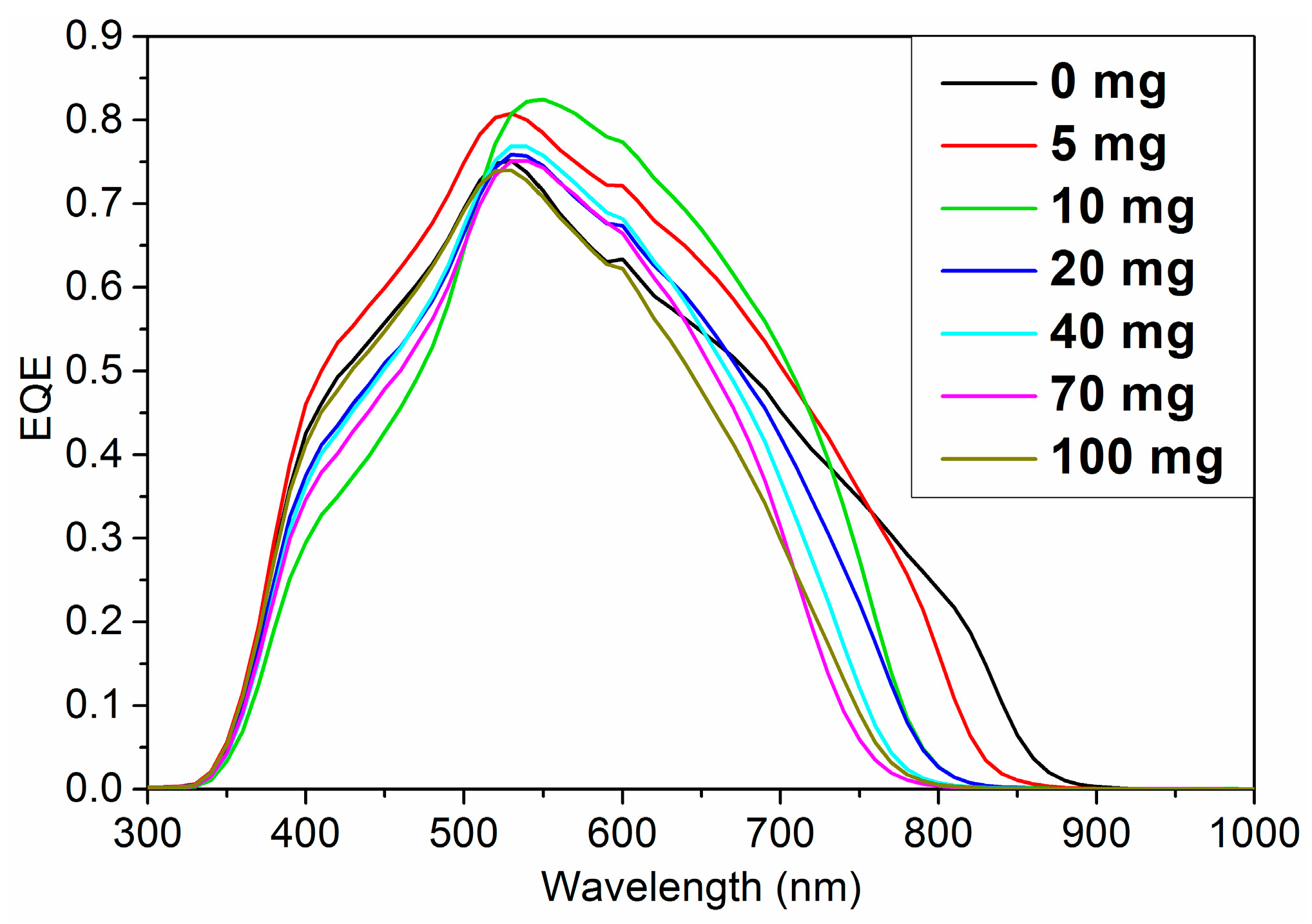
To understand this in more detail, the measurements of the external quantum efficiency (EQE) have to be considered (Figure 5). All samples show strong losses in the region between 450 and 500 nm due to the absorption of the CdS buffer layer. However, the reason for the differences between the individual samples in this wavelength region is not completely understood. One possible explanation is a changed Na concentration at the absorber surface, which is known to influence the CdS growth [23]. Additionally, the diffusion of, e.g., Cd into the absorber, which is known to influence the interface [24], might be different depending on the [S]/([S] + Se]) ratios. However, considerable differences in thickness are very unlikely since the growth can only be affected until the first monolayer of CdS has formed. The best carrier collection is achieved between 520 and 550 nm for all samples; in the longer wavelength region, the charge carrier collection is strictly declining. The reason might be the high number of grain boundaries that are suspected to act as recombination centers [25]. However, for CZTSSe, it was shown that larger grains do not necessarily improve the solar cell efficiency [26]. Additionally, the band gap (EG) can be estimated from the EQE measurements by plotting the squared EQE versus the energy. The results are displayed in Table 2 and show a gradual increase from 1.5 to around 1.7 eV.
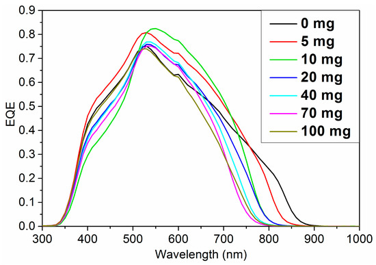
Figure 5.
EQE measurements of solar cells with CZGSSe absorbers that were annealed in the presence of different amounts of GeS as indicated by the labels.
Table 2.
[S]/([S] + [Se]) ratio, estimated band gap, VOC, VOC deficit and activation energy of the dominant recombination path for solar cells with CZGSSe absorbers that were annealed in the presence of different amounts of GeS. Band gap, VOC, and VOC deficit are determined from the same solar cell.
The VOC deficit that is commonly referred to as quality characteristic for solar cells with kesterite absorber can be calculated from Equation (1) (where q is the elementary charge):
The results are displayed in Table 2. In this series, the lowest VOC deficit of 868 mV could be obtained with 5 mg of GeS. However, this value is still much higher than for the most efficient CZTSSe absorber (617 mV [27]) and higher than the deficit of 656 mV that can be obtained for a CZGSe absorber with a band gap of 1.4 eV [4]. As band gap increases, the VOC deficit increases to values larger than 1 V, thereby drastically limiting the photovoltaic performance.
To understand the reason for this increased VOC deficit, temperature-dependent JV-characteristics have been measured in a temperature range between 5 and 65 °C. From a linear extrapolation of VOC to a temperature of 0 K, it is possible to estimate the activation energy of the dominant recombination path. If it is smaller than the band gap, this can be indicative of dominant recombination at the absorber–buffer interface [28,29]. The results for the activation energy EA are displayed in Table 2, and the corresponding plot can be found in the supplementary materials. For all samples, the activation energy is considerably smaller than the band gap, which suggests a strong interface recombination due to a non-ideal band alignment with the CdS buffer. With a larger absorber band gap, the difference between EA and EG considerably increases from 219 to 479 meV, which suggests that the band alignment between CdS and CZGSSe becomes worse and is the main reason for the decrease in photovoltaic performance as the [S]/([S] + Se]) ratio increases.
For further improvement of the solar cell efficiency, an optimization of all layers has to be taken into account. One possibility would be to replace the Mo back contact that is known to be thermodynamically instable [30] with other materials or add a suitable barrier layer between absorber and back contact. The absorber itself also needs to be optimized in terms of grain growth, and the use of a different buffer layer with proper band alignment might be especially promising, since an open-circuit voltage of more than 1 V was recently achieved with a high band gap CuGaSe2 absorber using a Zn1-xSnxOy buffer layer [31].
3. Materials and Methods
The CZGS precursors were prepared by doctor-blading a metal salt solution onto a molybdenum-coated soda lime glass substrate and a subsequent drying step. This procedure was repeated six times to build up a precursor film thickness of approximately 1 µm. The used solution consists of copper(I)-chloride, zinc(II)-chloride, germanium(IV)-chloride, and thiourea with dimethyl formamide as solvent. Further details about the metal salt solution can be found in Ref. [5]. In a second step, the precursor layer was annealed for 15 min at 550 °C in an Se-containing nitrogen atmosphere to induce grain growth and to exchange S for Se to form the CZGSSe absorber. The sample was placed inside a graphite box together with 300 mg of Se and a variable amount of GeS (0 mg, 5 mg, 10 mg, 20 mg, 40 mg, 70 mg, and 100 mg) to control the [S]/([S] + [Se]) ratio of the absorber. The cation composition was approximately [Cu]/([Zn] + [Ge]) = 0.7 and [Zn]/[Ge] = 1.0.
To obtain functional solar cells, the CZGSSe absorber was coated with chemical-bath-deposited CdS, a sputtered undoped ZnO and an aluminum-doped ZnO/Al layer. Further details can be found in Ref. [3].
Current–voltage curves were measured using a Keithley 2400 (Keithley Instruments, Solon, OH, USA) source measuring unit under simulated AM 1.5 global solar irradiation with a 2-lamp sun simulator (Wacom Electric, Tanaka, Japan) at 100 mWcm2. External quantum efficiency measurements were performed with a setup from Optosolar (Merdingen, Germany). X-ray diffraction measurements were performed with the model Empyrean from Panalytical (Almelo, Netherlands) in Bragg–Brentano geometry. The morphology of the absorbers was investigated with a scanning electron microscope (SEM, XL30 SFEG Sirion) from FEI Company (Hillsboro, OR, USA), using a 5 kV acceleration voltage. Raman spectra were obtained using a Vista Control confocal Raman microscope from Spectroscopy & Imaging (Warstein, Germany) with 488 nm, 457 nm, 442 nm, and 325 nm as excitation wavelengths.
4. Conclusions
In summary, Cu2ZnGeSxSe4-x absorbers with [S]/([S] + [Se]) ratios between 0.27 and 0.51 were synthesized by adding different amounts of GeS in the annealing step in an Se atmosphere. Thereby the band gap could be fine-tuned between 1.5 and 1.7 eV, which is an interesting range for top cell absorbers of multijunction solar cells. Detailed absorber characterization by XRD, SEM, and Raman microscopy confirmed the kesterite structure and did not show any indication of secondary phases. Furthermore, sulfoselenide Raman modes were detected and are reported here for the first time. All absorbers have been processed to functional solar cells. The efficiency declines as [S]/([S] + [Se]) ratio increases, but the open-circuit voltage was considerably increased. The VOC deficit remains a challenge. Further bulk and interface optimization will be necessary to increase efficiency and make these types of high-gap kesterites suitable for industrial application.
Supplementary Materials
The following are available online at www.mdpi.com/1996-1073/10/11/1813/s1, Figure S1: Detailed view of the MoSxSe2-x 100-reflection (a) with the reference positions for MoSe2 (JCPDS 065-3481) and MoS2 (JCPDS 37-1492) and the fitted reflection position versus the [S]/([S] + [Se]) ratio of the CZGSSe absorber (b). The position of the reflection is slightly shifted to higher diffraction angles with an increased S-incorporation into the absorber, while the intensity declines due to a reduced MoSxSe2-x layer thickness, Figure S2: The [S]/([S] + [Se]) ratio of the CZGSSe absorber and the MoSxSe2-x layer as determined from the XRD measurements according to Vegard’s law. For the calculation the 100 reflection positions of MoS2 (JCPDS 00-37-1492) and MoSe2 (JCPDS 03-065-3481) were used as reference and the shift of the Mo 110 reflection was corrected according to JCPDS 01-089-5156, Figure S3: Band gap and activation energy of the dominant recombination path for CZGSSe solar cells with different [S]/([S] + [Se]) ratios. The band gap EG was estimated by EQE, while the activation energy EA was determined from the extrapolation of VOC to 0 K. The temperature-dependent measurement of JV-characteristics was carried out in a temperature range between 5 and 65 °C, Figure S4: Plot of the squared quantum efficiency versus the energy to estimate the band gaps for CZGSSe absorbers that were processed in the presence of different amounts of GeS. Colored lines have been added as a guide to the eye, Figure S5: Box plots of fill factor (a) and short-circuit current density (b) of solar cells fabricated from CZGSSe absorbers that were annealed in the presence of different amounts of GeS, Figure S6: JV-characteristics under illumination of solar cells processed from samples that were annealed in the presence of 0–10 mg GeS (a) and 20–100 mg GeS (b).
Acknowledgments
This work was performed within the SWInG project that has received funding from the European Union’s Horizon 2020 research and innovation programme under grant agreement No. 640868.
Author Contributions
Mahmoud Seboui performed the sample preparation and characterization and evaluated the data. Thomas Schnabel assisted with data evaluation, conceived and designed the ideas, and wrote the paper. Erik Ahlswede helped to improve the paper’s quality.
Conflicts of Interest
The authors declare no conflict of interest. The founding sponsors had no role in the design of the study; in the collection, analyses, or interpretation of data; in the writing of the manuscript; or in the decision to publish the results.
References
- Buffiere, M.; ElAnzeery, H.; Oueslati, S.; Ben Messaoud, K.; Brammerth, G.; Meuris, M.; Poortmans, J. Physical characterization of Cu2ZnGeSe4 thin films from annealing of Cu-Zn-Ge precursor layers. Thin Solid Films 2015, 582, 171–175. [Google Scholar] [CrossRef]
- Khadka, D.B.; Kim, J. Study of structural and optical properties of kesterite Cu2ZnGeX4 (x = S, Se) thin films synthesized by chemical spray pyrolysis. CrystEngComm 2013, 15, 10500–10509. [Google Scholar] [CrossRef]
- Schnabel, T.; Seboui, M.; Bauer, A.; Choubrac, L.; Arzel, L.; Harel, S.; Barreau, N.; Ahlswede, E. Evaluation of different buffer materials for solar cells with wide-gap Cu2ZnGeSxSe4-x absorbers. RSC Adv. 2017, 7, 40105–40110. [Google Scholar] [CrossRef]
- Sahayaraj, S.; Brammerth, G.; Vermang, B.; Schnabel, T.; Ahlswede, E.; Huang, Z.; Ranjbar, S.; Meuris, M.; Vleugels, J.; Poortmans, J. Optoelectronic properties of thin film Cu2ZnGeSe4 solar cells. Sol. Energy Mater. Sol. Cells 2017, 171, 136–141. [Google Scholar] [CrossRef]
- Schnabel, T.; Seboui, M.; Ahlswede, E. Evaluation of different metal salt solutions for the preparation of solar cells with wide-gap Cu2ZnGeSxSe4-x absorbers. RSC Adv. 2016, 7, 26–30. [Google Scholar] [CrossRef]
- Timmo, K.; Kauk-Kuusik, M.; Altosaar, M.; Raudoja, J.; Raadik, T.; Grossberg, M.; Varema, T.; Pilvet, M.; Leinemann, I.; Volobujeva, O.; et al. Novel Cu2CdSnS4 and Cu2ZnGeSe4 absorber materials for monograin layer solar cell. In Proceedings of the 28th European Photovoltaic Solar Energy Conference and Exhibition, Villepinte, France, 30 September–4 October 2013. [Google Scholar]
- Shu, Q.; Yang, J.-H.; Chen, S.; Huang, B.; Xiang, H.; Gong, X.-G.; Wei, S.-H. Cu2Zn(Sn,Ge)Se4 and Cu2Zn(Sn,Si)Se4 alloys as photovoltaic materials: Structural and electronic properties. Phys. Rev. B 2016, 87, 115208-1–115208-6. [Google Scholar]
- Gershon, T.; Sardashti, K.; Gunawan, O.; Mankad, R.; Singh, S.; Lee, Y.S.; Ott, J.A.; Kummel, A.; Haight, R. Photovoltaic device with over 5% efficiency based on an n-type Ag2ZnSnSe4 absorber. Adv. Energy Mater. 2016, 6, 1601182. [Google Scholar] [CrossRef]
- Ge, J.; Yu, Y.; Yan, Y. Earth-abundant orthorhombic BaCu2Sn(SexS1-x)4 (x = 0.83) thin film for solar energy conversion. ACS Energy Lett. 2016, 1, 583–588. [Google Scholar] [CrossRef]
- Ge, J.; Yan, Y. Synthesis and characterization of photoelectrochemical and photovoltaic Cu2BaSnS4 thin films and solar cells. J. Mater. Chem. C 2017, 5, 6406–6419. [Google Scholar] [CrossRef]
- Lang, M.; Renz, T.; Mathes, N.; Neuwirth, M.; Schnabel, T.; Kalt, H.; Hetterich, M. Influence of the Cu content in Cu2ZnSn(S,Se)4 solar cell absorbers on order-disorder related band gap changes. Appl. Phys. Lett. 2016, 109, 142103. [Google Scholar] [CrossRef]
- Huang, L.; Deng, H.; He, J.; Meng, X.; Tao, J.; Cao, H.; Sun, L.; Yang, P.; Chu, J. Cu content dependence of morphological, structural and optical properties for Cu2ZnGeS4 thin films synthesized by sulfurization of sputtered precursors. Mater. Lett. 2015, 159, 1–4. [Google Scholar] [CrossRef]
- Vegard, L. Die konstitution der mischkristalle und die raumfüllung der atome. Z. Phys. 1921, 5, 17–21. [Google Scholar] [CrossRef]
- Guc, M.; Levcenko, S.; Izquierdo-Roca, V.; Fontane, X.; Arushanov, V.; Perez-Rodriguez, A. Polarized Raman scattering analysis of Cu2ZnSnSe4 and Cu2ZnGeSe4 single crystals. J. Appl. Phys. 2013, 114, 193514-1–193514-9. [Google Scholar] [CrossRef]
- Guc, M.; Izquierdo-Roca, V.; Perez-Rodriguez, A.; Gurieva, G.; Levcenko, S.; Schorr, S.; Arushanov, E. Raman spectra of wurtzstannite quaternary compounds. Phys. Stat. Solidi C 2013, 10, 1075–1078. [Google Scholar] [CrossRef]
- Grossberg, M.; Timmo, K.; Raadik, T.; Kärber, E.; Mikli, V.; Krustok, J. Study of structural and optoelectronic properties of Cu2Zn(Sn1-xGex)Se4 (x = 0 to 1) alloy compounds. Thin Solid Films 2015, 582, 176–179. [Google Scholar] [CrossRef]
- Khadka, D.B.; Kim, S.Y.; Kim, J. A nonvacuum approach for fabrication of Cu2ZnSnSe4/In2S3 thin film solar cell and optoelectronic characterization. J. Phys. Chem. C 2015, 119, 12226–12235. [Google Scholar] [CrossRef]
- Wiley, J.D.; Buckel, W.J.; Schmidt, R.L. Infrared reflectivity and Raman and scattering in GeS. Phys. Rev. B 1976, 13, 2489–2496. [Google Scholar] [CrossRef]
- Dimitrievska, M.; Xie, H.; Fairbrother, A.; Fontane, X.; Gurieva, G.; Saucedo, E.; Perez-Rodriguez, A.; Schorr, S.; Izquierdo-Roca, V. Multiwavelength excitation Raman scattering of Cu2ZnSn(SxSe4-x)4 polycrystalline thin films: Vibrational properties of sulfoselenide solid sulutions. Appl. Phys. Lett. 2014, 105, 031913. [Google Scholar] [CrossRef]
- Baer, M.; Weinhardt, L.; Heske, C.; Nishiwaki, S.; Shafarman, W.N. Chemical structures of the Cu(In,Ga)Se2/Mo and Cu(In,Ga)(S,Se)2/Mo interfaces. Phys. Rev. B 2008, 78, 075404. [Google Scholar] [CrossRef]
- Li, J.; Wei, M.; Du, Q.; Liu, W.; Jiang, G.; Zhu, C. The band alignment at CdS/Cu2ZnSnSe4 heterojunction interface. Surf. Interfaces Anal. 2013, 45, 682–684. [Google Scholar] [CrossRef]
- Gunawan, O.; Gokmen, T.; Warren, C.W.; Cohen, J.D.; Todorov, T.K.; Barkhouse, D.A.R.; Bag, S.; Tang, J.; Shin, B.; Mitzi, D.B. Band alignment at the Cu2ZnSn (SxSe1-x)4/CdS interface. Appl. Phys. Lett. 2011, 98, 253905-1–253905-4. [Google Scholar]
- Ren, Y.; Scragg, J.J.S.; Edoff, M.; Larsen, J.; Platzer-Björkman, C. Evolution of Na-S(-O) compounds on the Cu2ZnSnS4 absorber surface and their effects on CdS thin film growth. ACS Appl. Mater. Interfaces 2016, 8, 18600–18607. [Google Scholar] [CrossRef] [PubMed]
- Liu, F.; Ya, C.; Huang, J.; Sun, K.; Zhou, F.; Stride, J.A.; Green, M.A.; Hao, X. Nanoscale microstructure and chemistry of Cu2ZnSnS4/CdS interface in kesterite Cu2ZnSnS4 solar cells. Adv. Energy Mater. 2016, 6, 1600706. [Google Scholar] [CrossRef]
- Kim, G.Y.; Jeong, A.R.; Kim, J.R.; Jo, W.; Son, D.-H.; Kim, D.-H.; Kang, J.-K. Surface potential on grain boundaries and intragrains of highly efficient Cu2ZnSn(S,Se)4 thin-films grown by two-step sputtering process. Sol. Energy Mater. Sol. Cells 2014, 127, 129–135. [Google Scholar] [CrossRef]
- Schnabel, T.; Abzieher, T.; Friedlmeier, T.M.; Ahlswede, E. Solution-based preparation of Cu2ZnSn(S,Se)4 for solar cells—Comparison of SnSe2 and elemental Se as chalcogen source. IEEE J. Photovolt. 2015, 5, 670–675. [Google Scholar] [CrossRef]
- Wang, W.; Winkler, M.T.; Gunawan, O.; Gokmen, T.; Todorov, T.K.; Zhu, Y.; Mitzi, D.B. Device characteristics of CZTSSe thin-film solar cells with 12.6 efficiency. Adv. Energy Mater. 2014, 4, 1301465. [Google Scholar] [CrossRef]
- Turcu, M.; Pakma, O.; Rau, U. Interdependence of absorber composition and recombination mechanism in Cu(In,Ga)(Se,S)2 heterojunction solar cells. Appl. Phys. Lett. 2002, 80, 2598–2600. [Google Scholar] [CrossRef]
- Nadenau, V.; Rau, U.; Jasenek, A.; Schock, H.W. Electronic properties of CuGaSe2-based heterojunction solar cells. Part I. transport analysis. J. Appl. Phys. 2000, 87, 584–593. [Google Scholar]
- Scragg, J.J.; Wätjen, T.; Edoff, M.; Ericson, T.; Kubart, T.; Platzer-Björkman, C. A detrimental reaction at the molybdenum back contact in Cu2ZnSn(S,Se)4 thin-film solar cells. J. Am. Chem. Soc. 2012, 134, 19330–19333. [Google Scholar] [CrossRef] [PubMed]
- Larsson, F.; Nilsson, N.S.; Keller, J.; Frisk, C.; Kosyak, V.; Edoff, M.; Törndahl, T. Record 1.0 V open-circuit voltage in wide band gap chalcopyrite solar cells. Prog. Photovolt. Res. Appl. 2017, 25, 755–763. [Google Scholar] [CrossRef]


© 2017 by the authors. Licensee MDPI, Basel, Switzerland. This article is an open access article distributed under the terms and conditions of the Creative Commons Attribution (CC BY) license (http://creativecommons.org/licenses/by/4.0/).