Article

Energy Balance Control of a Cascaded Multilevel Inverter for Standalone Solar Photovoltaic Applications

School of Electric Power Engineering, South China University of Technology, Guangzhou 510641, China
*
Author to whom correspondence should be addressed.
Energies 2017, 10(11), 1805; https://doi.org/10.3390/en10111805
Submission received: 20 September 2017 / Revised: 27 October 2017 / Accepted: 2 November 2017 / Published: 9 November 2017
(This article belongs to the Section I: Energy Fundamentals and Conversion)

Abstract

:
This paper presents a clock phase-shifting (CPS) energy balance control (EBC) method for cascaded half-bridge multilevel inverters in standalone solar photovoltaic (PV) systems. It is based on the conservation of energy in each cascaded unit. By shifting the phase of the clock pulse of each cascaded unit, a staircase-like output voltage is obtained. The CPS EBC not only regulates the staircase-like output voltage of the cascaded multilevel inverters accurately under static conditions, but also suppresses the fluctuations of DC sources and improves its dynamic responses to load steps. Thus, the problems existing in solar PV systems using the cascaded multilevel inverters are avoided. Results obtained from simulations and experiments are presented to verify the feasibility and advantages of the proposed control method.

1. Introduction

Renewable energy sources are becoming increasingly important for electricity generation, since non-renewable energy sources such as fossil fuels are facing serious problems, e.g., pollutions, uncertain future of fossil-fuel prices, being unsustainable and CO2 emissions [1]. Among these alternative energy sources, solar energy has been identified as being clean and easily available [2]. However, DC power produced by PV modules is not compatible with standard electrical appliances operating with AC power. In order to be compatible with the standard AC electrical appliances, various inverter topologies are proposed and employed to convert the DC electricity to the AC form [1]. Among these topologies, multilevel inverters have been receiving much attention, the most popular of them being cascaded multilevel inverter topologies [3,4], diode-clamped multilevel inverter topologies [5,6] and flying-capacitor multilevel inverter topologies [7,8]. A comparative analysis of the three topologies demonstrates that the cascaded topology is simple and uses the least components. Also, the cascaded topology is ideally suited for solar PV systems, where isolated input DC sources are available. Therefore, the cascaded topology is considered as the most suitable for solar PV systems in all multilevel topologies. 
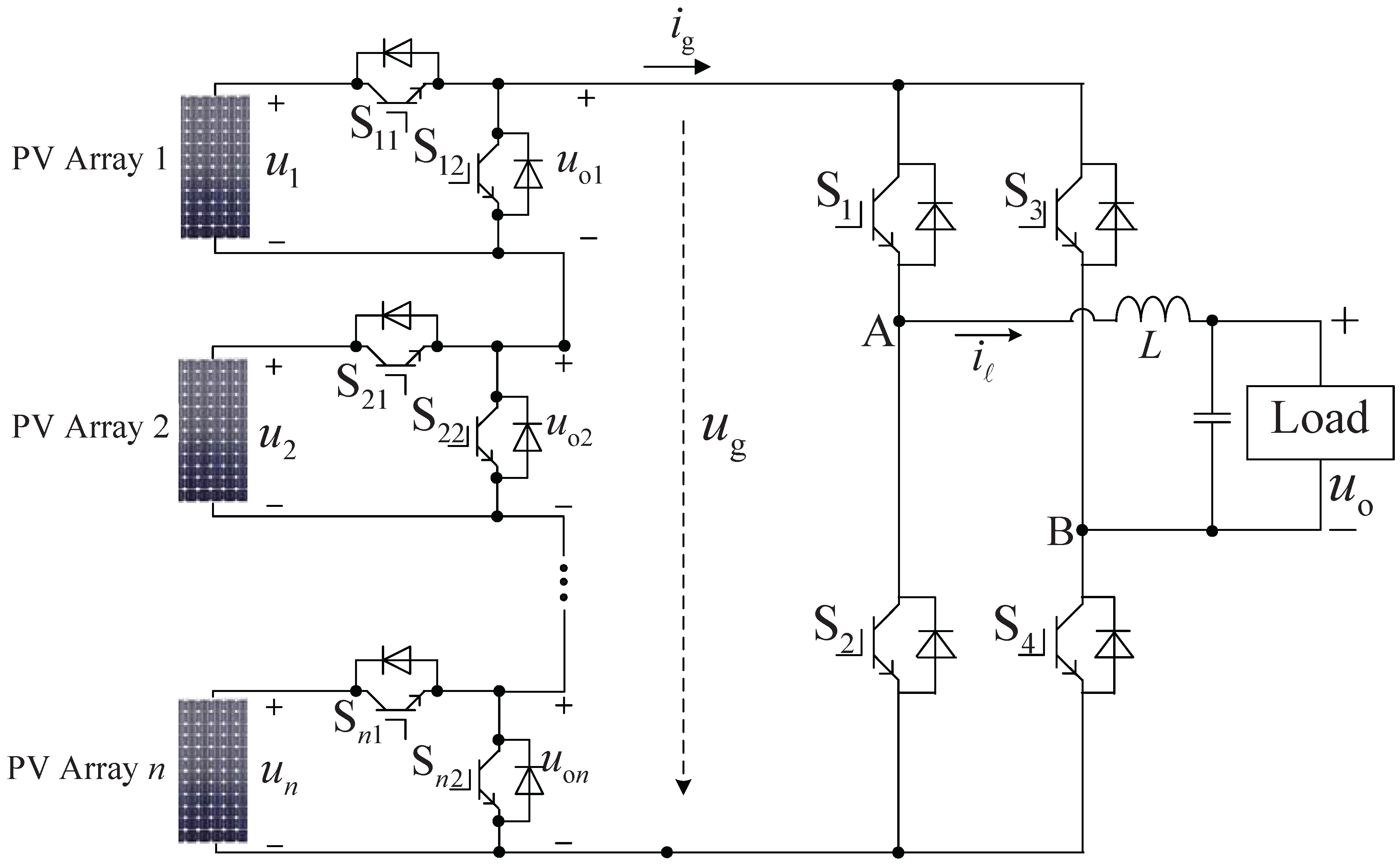
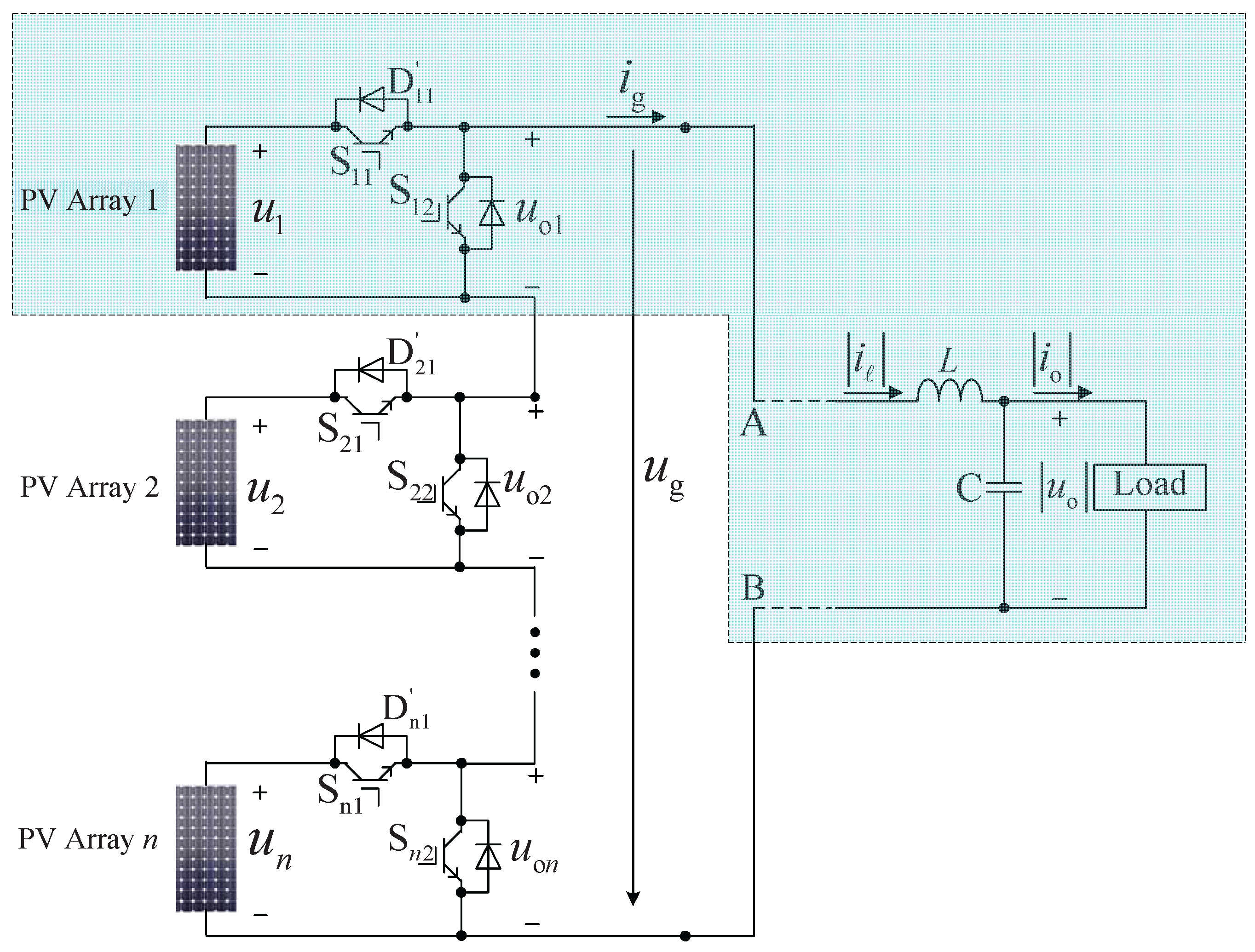
Figure 1 displays the block diagram of a standalone solar PV system using a cascaded half-bridge multilevel inverter [9]. Compared with the typical cascaded H-bridge (CHB) multilevel topology, the cascaded half-bridge multilevel topology reduces nearly half the number of required switches. Recently, a cascaded switched-diode topology has been proposed [10,11]. The comparison with cascaded half-bridge multilevel topology illustrates that more voltage levels are produced with fewer required switches. However, under a case of resistance-inductance (R-L) loads, high voltage spikes occur at the base of the stepped output voltage due to the lack of a path for reverse load currents, which tend to deteriorate power quality [12].
Basic modulations techniques for cascaded multilevel topologies are rooted on the fundamental frequency switching [9], sinusoidal pulse width modulation (PWM) [13,14], and space vector PWM (SV-PWM) [15]. However, in solar PV systems, DC sources of a multilevel inverter topology are supplied by PV modules, as shown in Figure 1, which brings about a series of problems:
  • Power imbalance: the power of a PV array supplied to each cascaded unit of the multilevel inverter may be different, introduced by cloud shading, different irradiance levels and ambient temperatures.
  • DC supply with fluctuations: the DC supply from a PV array is always with fluctuation caused by variety of external factors, such as illumination change, shadow, ambient temperature and etc. More specifically, following variations in a certain range of irradiance level will lead to the instability of the voltage, which manifests as low frequency pulsation.
  • Load variations: with the constant expansion of application fields, loads of an inverter are becoming more and more diversified. Abrupt load variations happen regularly.
The existence of these problems cause distortions or bring lots of low harmonics to the output voltages of the cascaded multilevel inverters using basic modulation techniques, which leads great hazards to electrical equipment. In recent years, some nonlinear control methods, e.g., hysteresis control, sliding mode control, fuzzy logic control and so on, have been attempted in multilevel inverters. As presented in [16], the advantages of using various accessible DC voltage levels have been fully exploited by using the hysteresis control. Sliding-mode control (SMC), as presented in [17], provides fast dynamic responses. However, the variable switching frequency and nonzero steady-state error are the drawbacks of these methods. Then in [18], a fuzzy logic control has been proposed. The dynamic behaviours are improved by considering moving cloud obfuscating the PV arrays.
Among the problems in solar PV systems, the power imbalance can be classified into two categories: (1) the inter-phase power imbalance, which occurs when each phase generates different amount of power; and (2) the inter-bridge power imbalance, which happens when each bridge in the same phase generates different amounts of power [19]. A three-phase system focus more on the interphase power imbalance because three-phase unbalanced currents result in wasted power. New control methods [19,20] or converter topology [21] have been proposed to deal with the interphase power imbalance problem of CHB converters in PV systems. In contrast, the interbridge power imbalance gets more attention in single-phase systems. A continuous time-domain power balancing control algorithm was presented to solve the interbridge imbalance of a single-phase CHB converter [22]. However, this method can improve but not completely suppress fluctuations of the DC supply of the multilevel inverter. Thus, the problem of DC supply with fluctuations in PV application has not been solved. A CPS one-cycle control method was proposed for multilevel inverters. While its inhibitory capability to the interbridge power imbalance and variations of input voltage is satisfactory, the inhibitory capability to load changes is still poor [12].
The objective of this paper is to verify the ability of the proposed CPS EBC method to deal with the problems of a multilevel inverter in standalone solar PV applications. The basic structure of this paper is as follows. Section 2 introduces the cascaded half-bridge topology. The derivation of the control equation, the design and implementation of the proposed CPS EBC method are illustrated in Section 3. Section 4 presents the simulation and experimental results. Final conclusions are given in Section 5.

2. Topology of the Cascaded Half-Bridge Multilevel Topology

Figure 1 displays the cascaded half-bridge topology for standalone solar PV applications. The topology is divided into two stages. The first stage is cascaded by n half-bridge converters. The cascaded unit, e.g., unit 1, as shown in Figure 1, contains a DC source supplied from a PV array, the DC voltage of which is equal to u 1 , switches S 11 and S 12 . The output of the unit 1 u o 1 have two values, which are u 1 when switch S 11 conducts and S 12 is off, and when switch S 11 is off and S 12 is turned on, the value of u o 1 is 0. For states of switches S 11 , S 12 , S 21 , S 22 , ⋯, S ( n 1 ) 1 , S ( n 1 ) 2 , S n 1 S n 2 , the output voltage of the first stage u g obtains 2 n different values, as listed in Table 1, the maximum of them is given as follows:
u g = u o 1 + u o 2 + + u o n .
From Table 1, it can be observed that the first stage generates a positive output voltage. For generating both positive and negative values, the second stage, which is a full-bridge inverter, is required. Table 2 lists the obtained output voltage u o under different switch states. Through the judgement of the positive or the negative sign of a reference voltage u ref , both the positive and negative halves of u o are achieved.
Under the symmetric case, that is, all the DC sources are equal to u dc , the total number of required switches N IGBT against the output voltage levels N level are shown as follows,
N IGBT = N level + 3 .
Compared with the CHB multilevel topology ( N IGBT = 2 ( N level 1 ) ), the cascaded half-bridge multilevel topology reduces nearly half the number of required switches. However, in designing such a multilevel topology, it should be noted that the switches of the full-bridge converter S 1 , ⋯, S 4 have to withstand the total voltage of all cascaded units, while the switches of the first stage S 11 , S 12 , ⋯, S n 1 , S n 2 only withstand a fraction of the total voltage of all cascaded units. This indicates that the four switches in the full-bridge cell of the second stage are with a high capability of the voltage rating, which makes the total voltage rating increase and leads to the limitation of the high voltage applications. Thus, the cascaded half-bridge multilevel topology is more suitable for medium voltage ( 2.3 , 3.3 , 4.16 or 6.9 kV ) applications [23].

3. The CPS EBC Method for Cascaded Half-Bridge Multilevel Topology

3.1. The Design of the CPS EBC

According to the topology analysis in Section 2, the second stage implements the generation of the positive and negative halves of output voltage by comparing the reference voltage u ref with zero. Thus, the second stage in Figure 1 can be omitted. Then a topology is constructed for the design of the CPS EBC, as shown in Figure 2. Compared with Figure 1, it can be seen that the second stage is omitted.
Figure 3 shows the structure of the proposed CPS EBC method to control the topology shown in Figure 2. The structure displays that a CPS EBC contains n independent EBC controllers. Each independent EBC controller corresponds to a cascaded unit, for instance, the EBC controller 1 in Figure 3 is used for controlling cascaded unit 1, which is the part of the dotted box in Figure 2. The n independent EBC controller are similar but with a T s / n phase-shift of the clock pulse, where T s denotes the switching cycle of the multilevel inverter. For an example of cascaded unit 1, the control equation of the EBC controller 1 is derived as follows. From Figure 2, it can be seen that the part of the dotted box can be regarded as a buck circuits: the circuit, constructed by u 1 , S 11 , S 12 , L, C. Then similar to that of [24], the control principle of the EBC controller 1 is that, by keeping the balance between the energy injected into the circuit from DC sources W in 1 ( k ) and the sum of the output energy W out 1 ( k ) and the energy the inductor L stores Δ W ( k ) in a switch cycle, e.g., the k th switching cycle [ ( k 1 ) T s , k T s ) [24], the EBC controller forces the output voltage to be a desired value , as
W in 1 ( k ) = W out 1 ( k ) + Δ W ( k ) ( k = 1 , 2 , )
During the k th switching cycle, the part of the dotted box in Figure 2 operates as a buck converter in two states. In state 1, S 11 is on for the duration t on 1 ( k ) . In this switching state, DC sources injects energy into the circuit and i g = | i | flows through the loop ( u 1 S 11 L C R S n 2 S ( n 1 ) 2 S 22 u 1 ). L is charged, and R consumes energy, then u o 1 is obtained using
u o 1 ( t ) = u 1 ( t [ ( k 1 ) T s , ( k 1 ) T s + t on 1 ( k ) )
In state 2, S 11 is turned off and S 12 is on for the duration t off 1 ( k ) . In this switching state, no energy is fed into the circuit, and i g = | i | flows through the loop ( S 12 L C R S n 2 S ( n 1 ) 2 S 12 ). L is discharged, and R consumes energy. Then u o 1 is obtained using
u o 1 ( t ) = 0 ( t [ ( k 1 ) T s + t on 1 ( k ) , k T s )
The above analysis of the operation states illustrates that the DC source u 1 of the cascaded unit 1 works in the time interval [ ( k 1 ) T s , ( k 1 ) T s + t on 1 ( k ) ), while L and R operate in the entire switching cycle. The energy values of W in 1 ( k ) , W out 1 ( k ) and Δ W 1 ( k ) during the k th switching cycle are calculated as follows:
W in 1 ( k ) = ( k 1 ) T s ( k 1 ) T s + t on 1 ( k ) u 1 ( t ) i g ( t ) d t
as i g = | i ( t ) | , then W in 1 ( k ) is derived as below:
W in 1 ( k ) = ( k 1 ) T s ( k 1 ) T s + t on 1 ( k ) u 1 ( t ) | i ( t ) | d t
W out 1 ( k ) = ( k 1 ) T s ( k 1 ) T s + T s | u ref 1 ( t ) i o ( t ) | d t
Δ W 1 ( k ) is calculated as the following:
Δ W 1 ( k ) = ( k 1 ) T s ( k 1 ) T s + T s | u ( t ) i ( t ) | d t
Substituting the values of W in 1 ( k ) , W out 1 ( k ) and Δ W ( k ) into (3) derives:
( k 1 ) T s ( k 1 ) T s + t on 1 ( k ) u 1 ( t ) | i ( t ) | d t = | u ref 1 i o ( t ) | T s + ( k 1 ) T s k T s | u ( t ) i ( t ) | d t ( k = 1 , 2 , )
Combining the aforementioned state analysis, (10) can be realized by controlling u o 1 , which is expressed in
( k 1 ) T s k T s u o 1 ( t ) | i ( t ) | d t = | u ref 1 i o ( t ) | T s + ( k 1 ) T s k T s | u ( t ) i ( t ) | d t ( k = 1 , 2 , )

3.2. The Implementation of CPS EBC

As a part of the control reference, | u ref 1 i o ( t ) | T s is calculated instantaneously. The other part ( k 1 ) T s k T s | u ( t ) i ( t ) | d t is calculated in the instant of the beginning of the k th switching cycle and kept the same during the entire switching cycle. Note here, the value of ( k 1 ) T s k T s | u ( t ) i ( t ) | d t is collected only in the time point k th T s , thus there is a switching cycle lag. The errors due to this switching cycle lag are ignored here, since the duration of the switching cycle is short. This means that the value used in the k th switching cycle is actually the value obtained in the ( k 1 ) th switching cycle.
After the computation of the control reference, the CPS EBC method is implemented with comparison and integration as shown in Figure 3. Here, the implementation of the EBC controller 1 is described as follows. When S 11 is turned on by a clock pulse with fixed frequency, the integral operation starts and u o 1 ( t ) = u 1 . Thus the output of the integrator W int 1 ( t ) is calculated as follows:
W int 1 ( t ) = ( n 1 ) T s t u o 1 ( t ) | i ( t ) | d t = ( n 1 ) T s t u 1 | i ( t ) | d t
as time goes on, W int 1 ( t ) increases from its initial value and is compared with the control reference instantaneously. At the instant when W int 1 ( t ) reaches W out 1 ( k ) + Δ W 1 ( k ) , a reset pulse is generated by the comparator to reset the RS flip-flop to be ( Q = 0 ). Then S 11 is turned off, while S 12 is turned on. At the same time, W int 1 ( t ) is reset to zero. The switching state is kept until the arrival of the next clock pulse, which starts the ( k + 1 ) th switching cycle.
As the design and implementation for other EBC controllers are similar to that of the EBC controller 1, the details are not presented here.

4. Simulation and Experimental Results

When designing solar PV fed inverters, the estimation of PV characteristics and maximum power point tracking (MPPT) control are one focus for solar PV modelling, meanwhile another way to simulate PV arrays employs a DC power supply with variable output voltage. Concerning stand-alone PV systems, the extraction of energy from PV arrays depends on the load demand [18,25]. In this research, on the premise of guaranteeing the installed output power of PV arrays, each PV array is only simulated by a V-I characteristic with an open-circuit voltage that is equal to 80 V . It should be noticed that the PV modelling method employed in this research cannot represent the PV arrays controlled by a MPPT algorithm. At first, a five-level and nine-level two-stage half-bridge multilevel inverter with a switching frequency of 2,500 Hz are set up. The parameters are u 1 = u 2 = = u n = 80 V , R = 50 Ω , L = 16 mH , C = 10 μ F , u ref 1 = u ref 2 = = u ref n = 60 V 
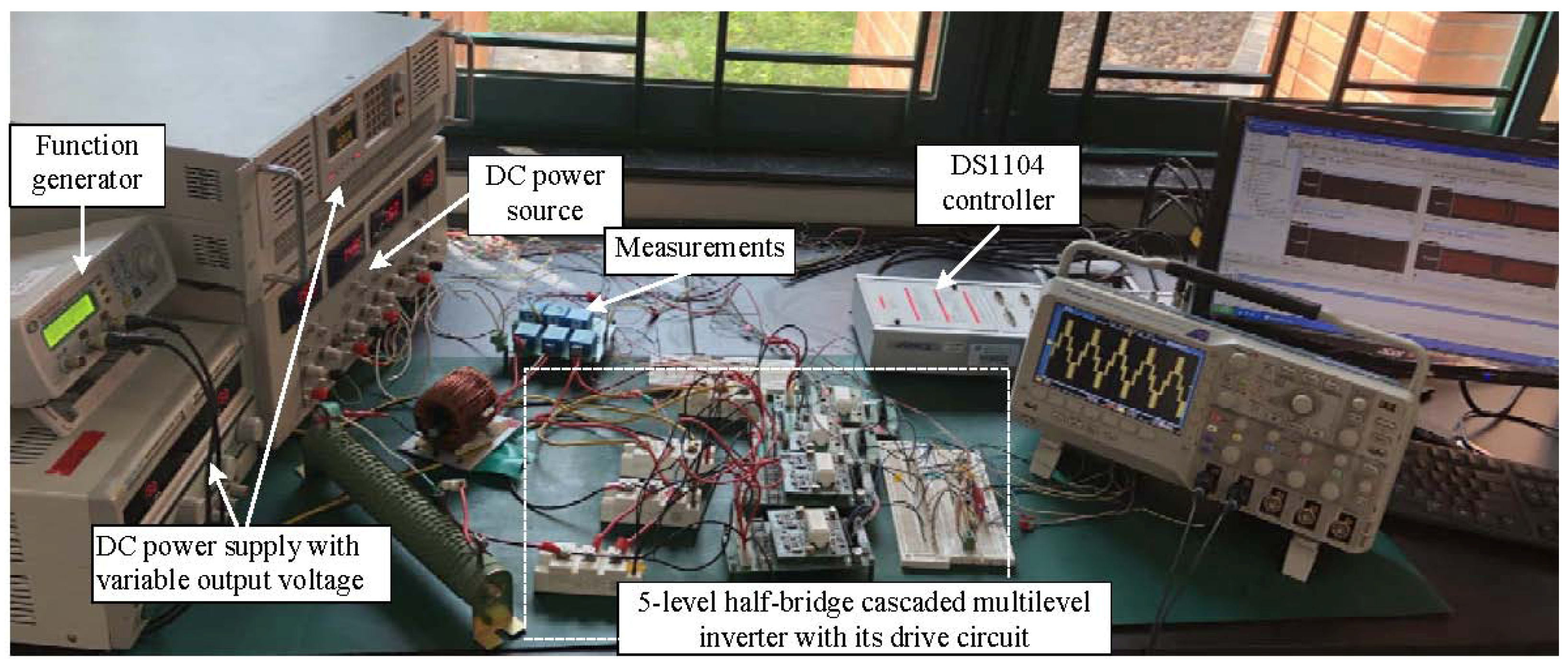
. Then a five-level experimental prototype, the parameters of which are identical with that of the simulation model, is built. In the experimental prototype shown in Figure 4, the voltage and current are sampled by the measurement, which is made up of HALL voltage sensors CHV-25P/100 (Measurement range: 0– ± 150 V ; Measurement accuracy: ± 0.1 % ) and HALL current sensors CHB-25NP/6 A (Measurement range: 0– ± 9 A ; Measurement accuracy: ± 0.8 % ), respectively. The gate drivers of the IGBT are configured on SKYPER 32R (SEMIKRON, Nuremberg, Germany), which are powered with the DC power source ( 0 / 15 V 
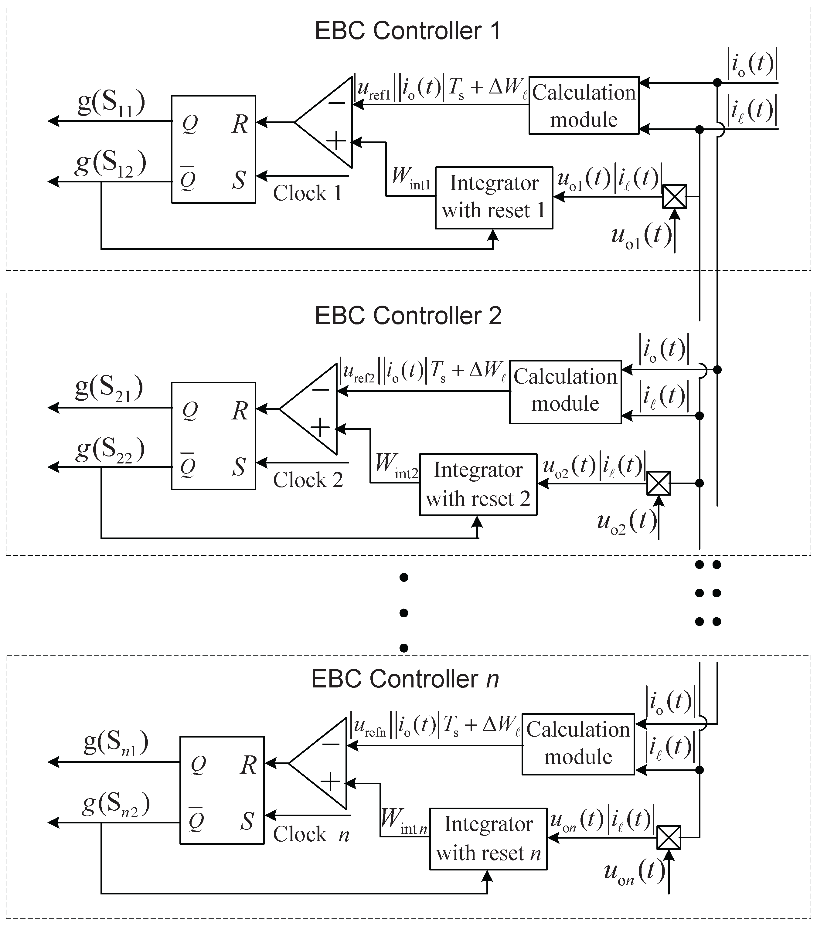
). In the experiment, PV arrays are emulated by DC power with variable output voltage and a function generators. The function generator TFG1900B (Suin Instuments, Nanjing, China) is connected in series with the DC power, which generate fluctuations (here is the low frequency ripples) to simulate the variations in irradiance and temperature of PV array outputs. The overall control strategy is implemented on a DS1104 (dSPACE company, Padbourne, Germany) system, where the proposed CPS EBC controller was programmed for the five-level half-bridge cascaded multilevel inverter.
To reveal the limitations of the conventional controller for solar PV applications, a carrier phase-shifted sinusoidal pulse width modulation (CPS SPWM) controller is configured. Although in recent years some nonlinear control methods have been attempted for controlling multilevel inverters, the CPS SPWM controller based on the sinusoidal PWM is still the most typical modulation strategy in cascade multilevel converter applications, as the CPS SPWM has the advantages of low-switching technique, balancing switching loads and good harmonic characteristics. The comparative studies demonstrate the ability to suppress DC source fluctuations and the improved dynamic responses to load variations using the CPS EBC. A comparison is made with the CPS SPWM because it is most frequently used for controlling cascaded multilevel inverters.

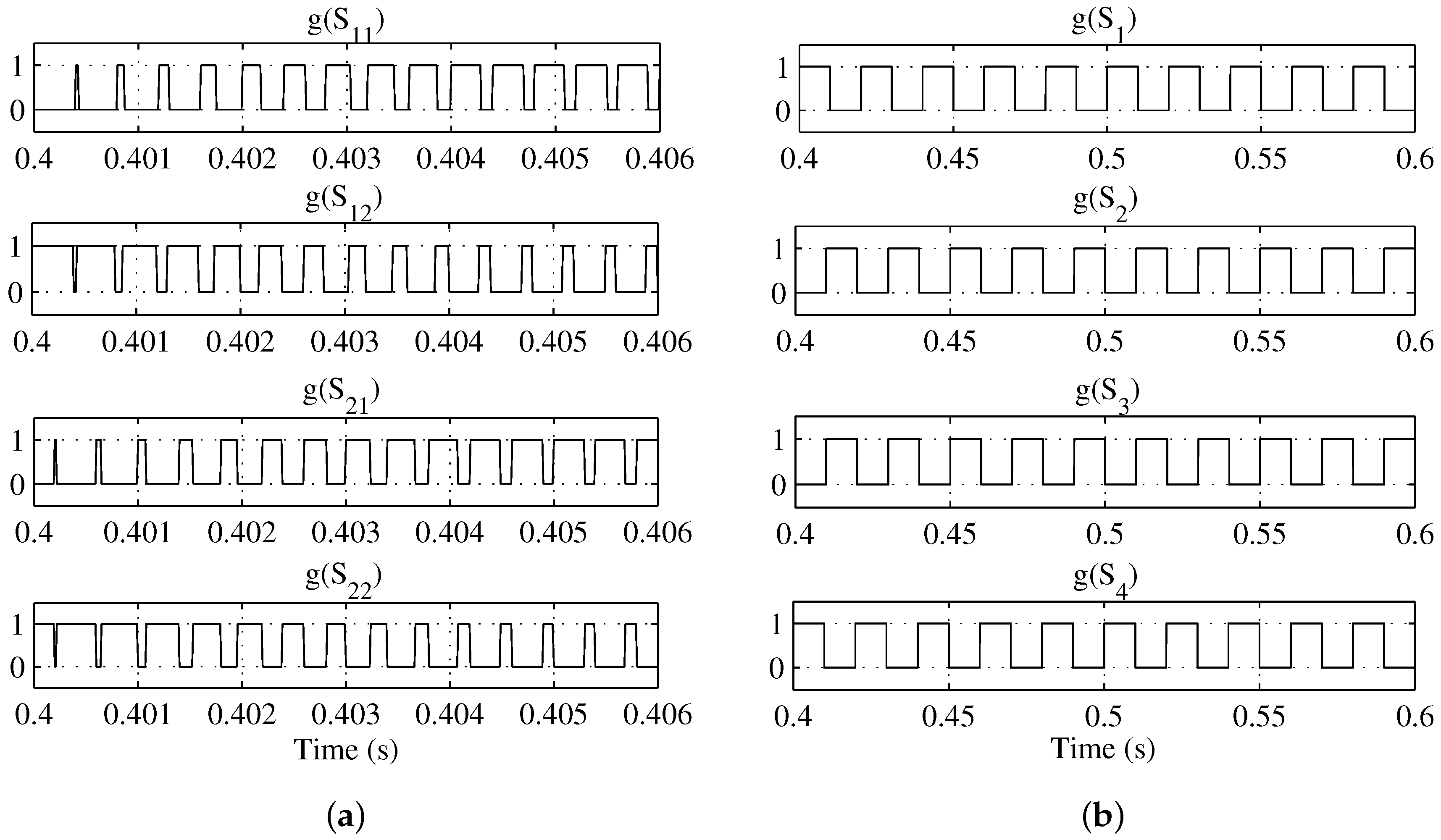
4.1. The Operation of CPS EBC

Figure 5 shows the gate signals of the cascaded half-bridge multilevel inverter. From Figure 5a, it can be seen that when S 11 is on, S 21 is off; When S 11 is turned off, S 21 is on. The gate signals of the second stage are shown in Figure 5b. S 1 and S 4 are on-state when u ref 0 . In this switching state, u o = u g . When u ref < 0 , S 1 and S 4 are turned off and S 2 and S 3 are turned on. In this switching state, u o = u g for the negative half cycle. By judging the sign of u ref , both the positive and negative halves of output voltage are obtained.
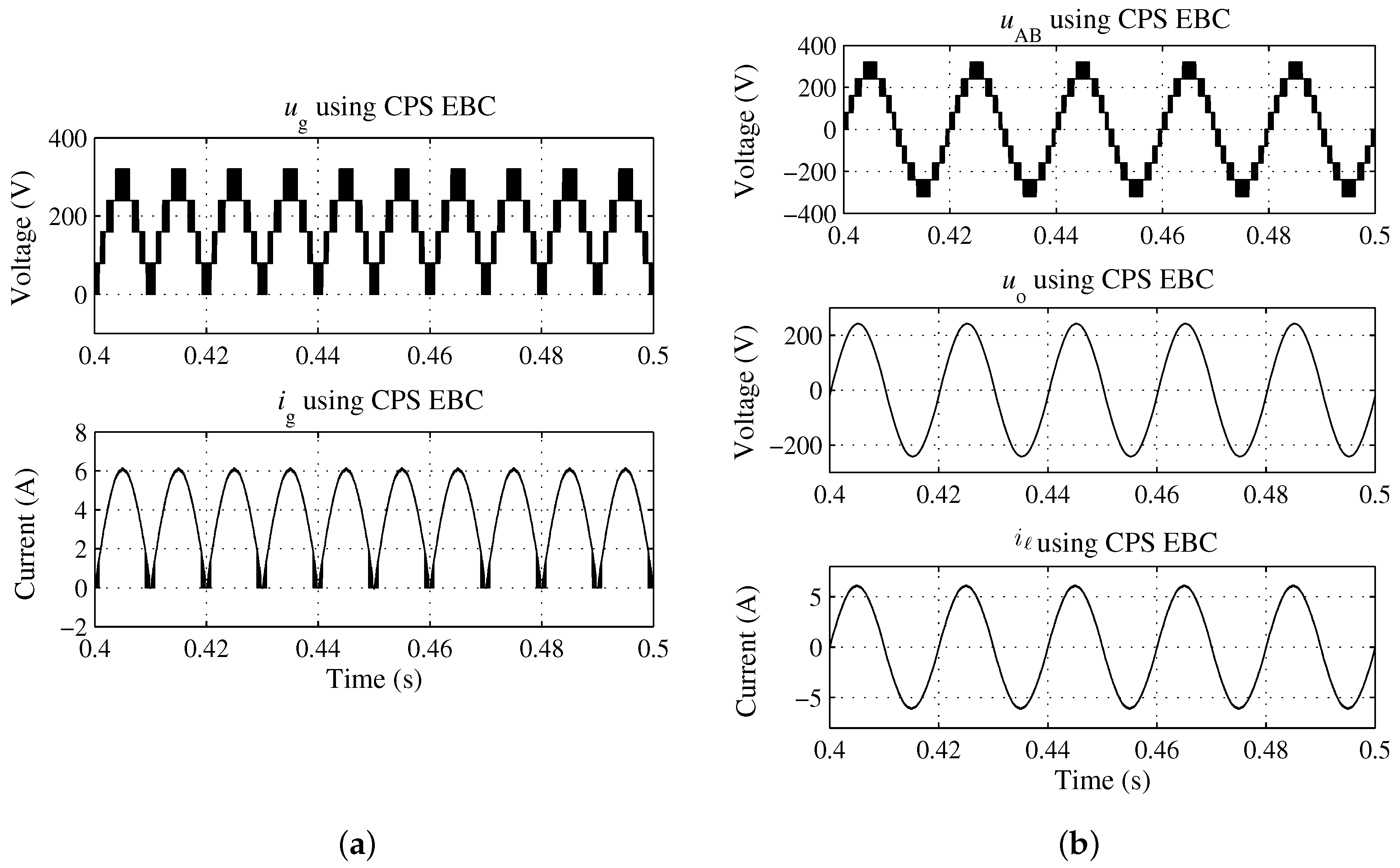
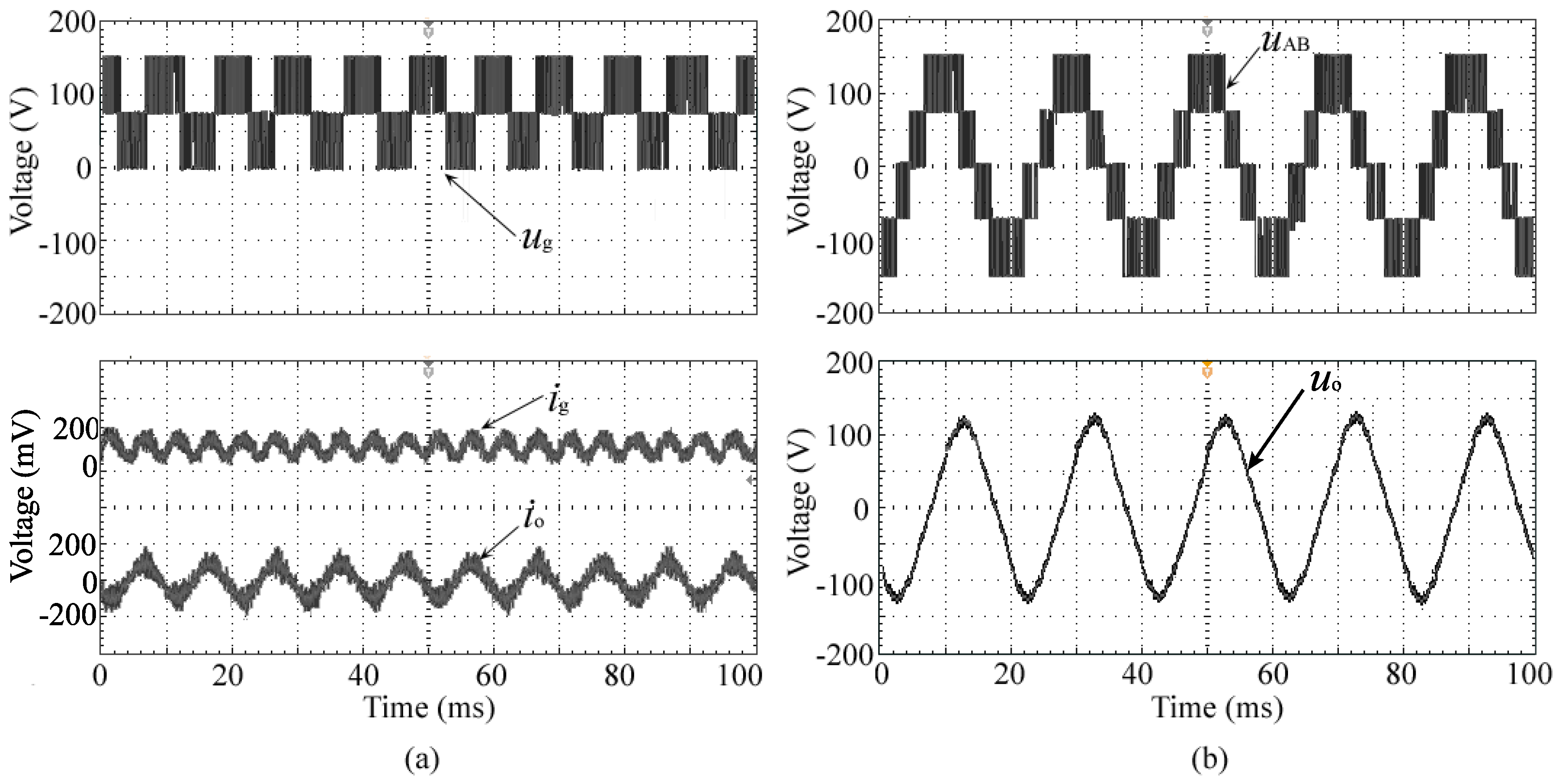
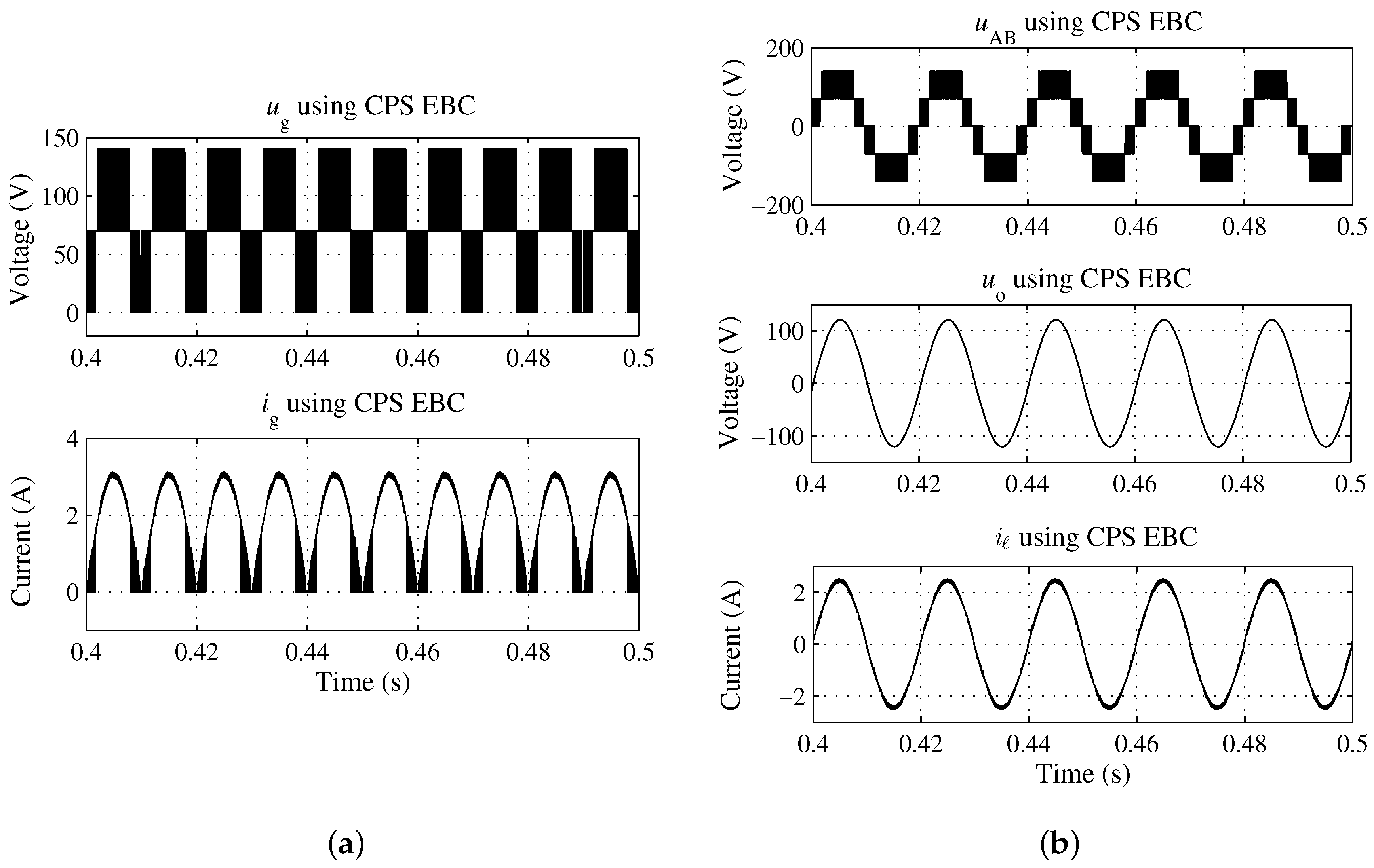
As shown in Figure 6a, the output of the first stage u g , which is the sum of the output voltage of all the cascaded units, has positive and zero values. The output current i g of the first stage is also positive. The voltage between points A and B u AB , the output voltage u o and the inductor current i of the multilevel inverter are shown in Figure 6b. From the waveforms in the figure, it can be seen that u AB is a staircase waveform with a frequency of 50 Hz and an amplitude of 160 V . After the ( L C ) filter, u o and i are almost sinusoidal waveforms. 
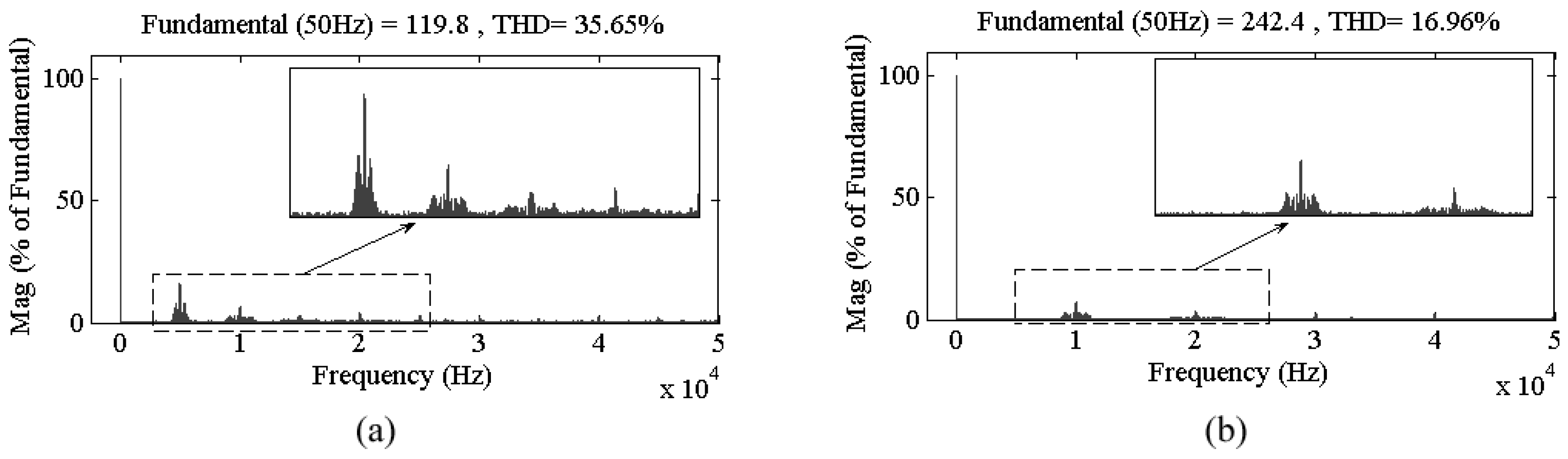
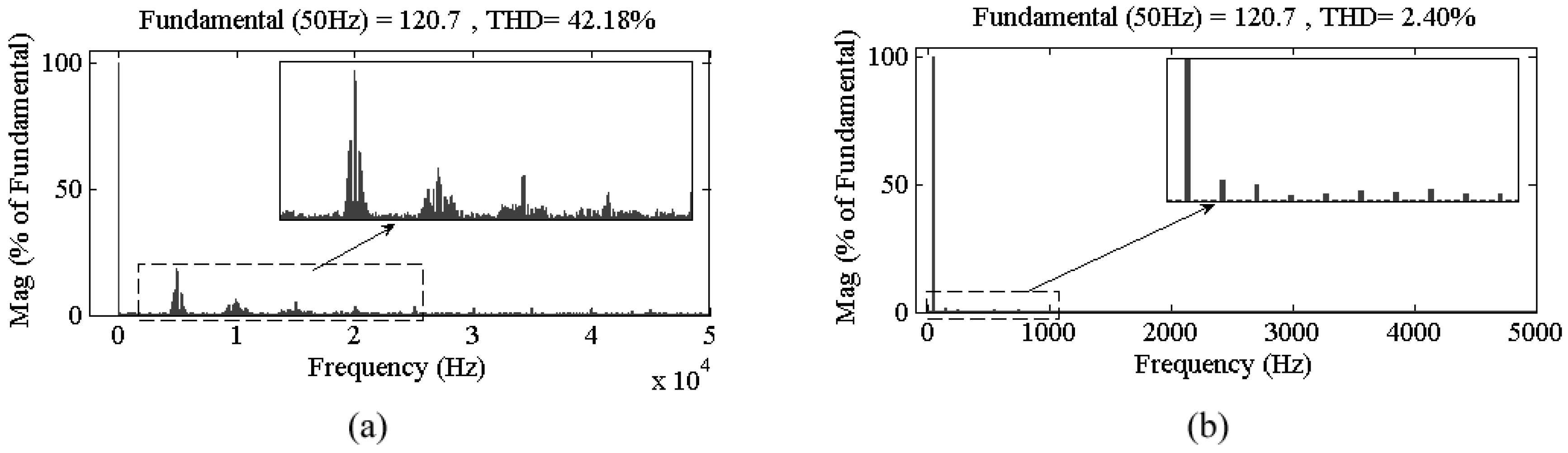
Figure 7a demonstrates that the total harmonic distortion (THD) of u AB of the five-level simulation prototype is 35.65% and the frequencies that the main harmonics focus on is multiples of 5000 Hz (5000 Hz , 10,000 Hz , 15,000 Hz , ), where 5,000 Hz is twice of the switching frequency (2500 Hz ).
Figure 8 illustrates the simulation results of the operation of a nine-level multilevel topology. It is observed from Figure 8a that u g and i g have zero and positive values. Figure 8b shows the waveforms of u AB , u o and i of the nine-level multilevel topology. The waveforms in the figure demonstrate that u AB is a staircase waveform with a frequency of 50 Hz and an amplitude of 320 V . After the ( L C ) filter, u o and i are almost sinusoidal waveforms. The THD of u AB of the nine-level multilevel inverter is 16.96%, as shown in Figure 7b. The frequencies that the main harmonics focus on is multiples of 10,000 Hz (10,000 Hz, 20,000 Hz, 30,000 Hz,…), where 10,000 Hz is four times of the switching frequency 2500 Hz. The comparison with THD of u AB of the five-level prototype, the THD is reduced and the frequencies that the main harmonics focus on move backward, which reduces the designing standards of the output filter.
The experimental results of the five-level prototype using the CPS EBC are shown in Figure 9 and Figure 10. The figures illustrate that the results are consistent with the simulation results in Figure 6. u g and i g of the first stage are positive. u AB is a five-level staircase waveform. The THD of u AB is 42.18% and the frequencies that the main harmonics focus on is (5000 Hz, 10,000 Hz, 15,000 Hz, …) , as shown in Figure 10a. After the ( L C ) filter, u o and i are sinusoidal waveforms. The THD of u o is 2.40%, as shown in Figure 10b.
The above simulation and experimental results verify the feasibility of the CPS EBC method for the cascaded half-bridge multilevel inverter in standalone solar PV applications.

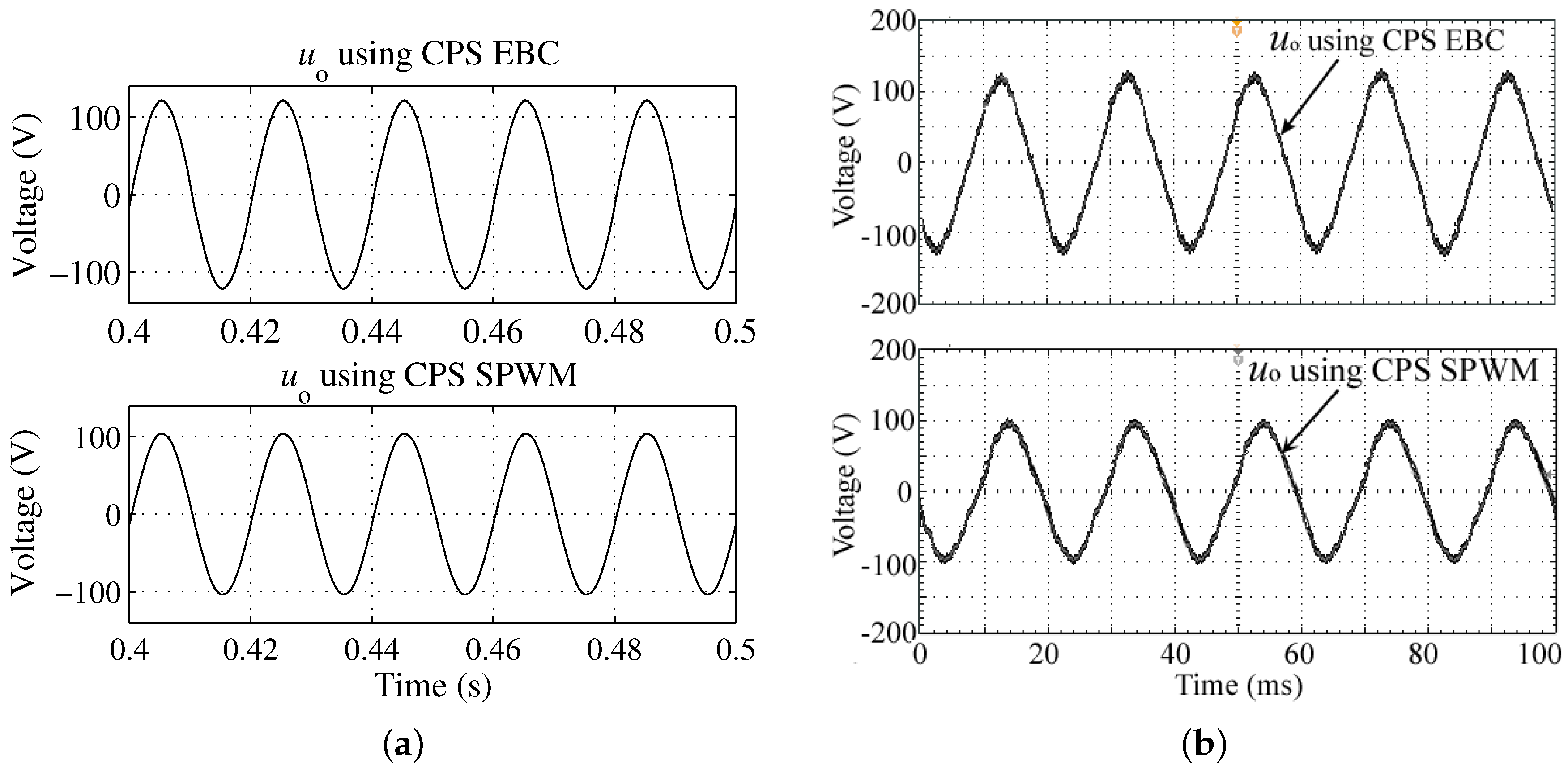
4.2. The Suppression Ability of the CPS EBC against Interbridge Power Imbalance in DC Sources

To evaluate the ability of the CPS EBC to suppress the power imbalance of the PV arrays, DC sources ( u 1 , u 2 , , u n ) are designed by different DC voltages. The simulation and experimental results are demonstrated in Figure 11.
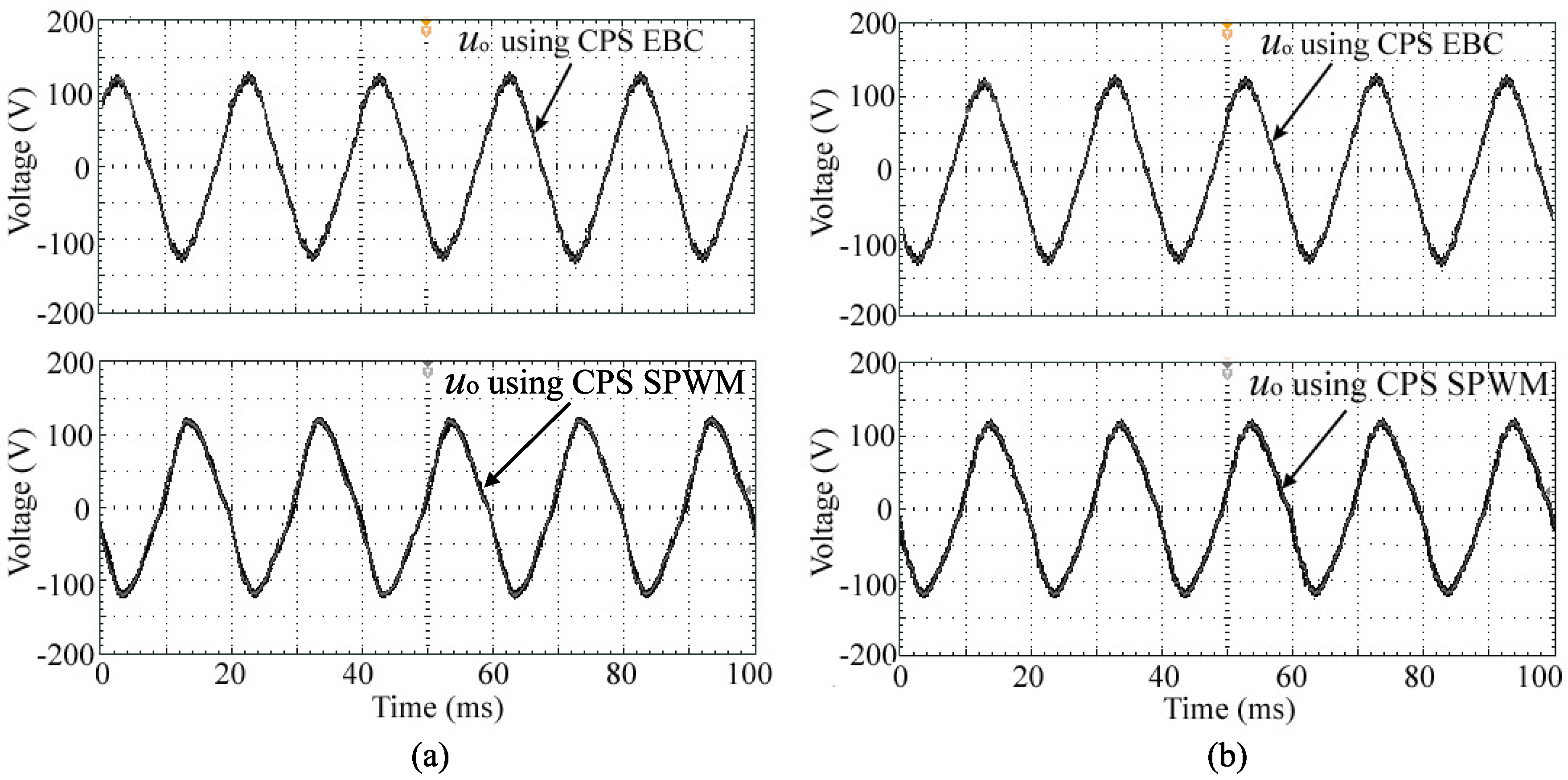
Figure 11a shows the simulation results under power imbalance (under the obfuscation of cloud shadowing, the PV unit 1 ( u 1 ) is with a voltage drop 15 V ). The comparison results demonstrate that u o using CPS SPWM tracks its reference 120 V with a drop 18 V . In contrast, u o using CPS EBC tracks its reference with no voltage drop. Figure 11b display the experimental results using the CPS EBC and the CPS SPWM under the cases of power imbalance. From the comparisons, it can be observed that the experimental results are consistent with the simulation results in Figure 11a. Thus the ability of the proposed CPS EBC against the interbridge power imbalance is verified.

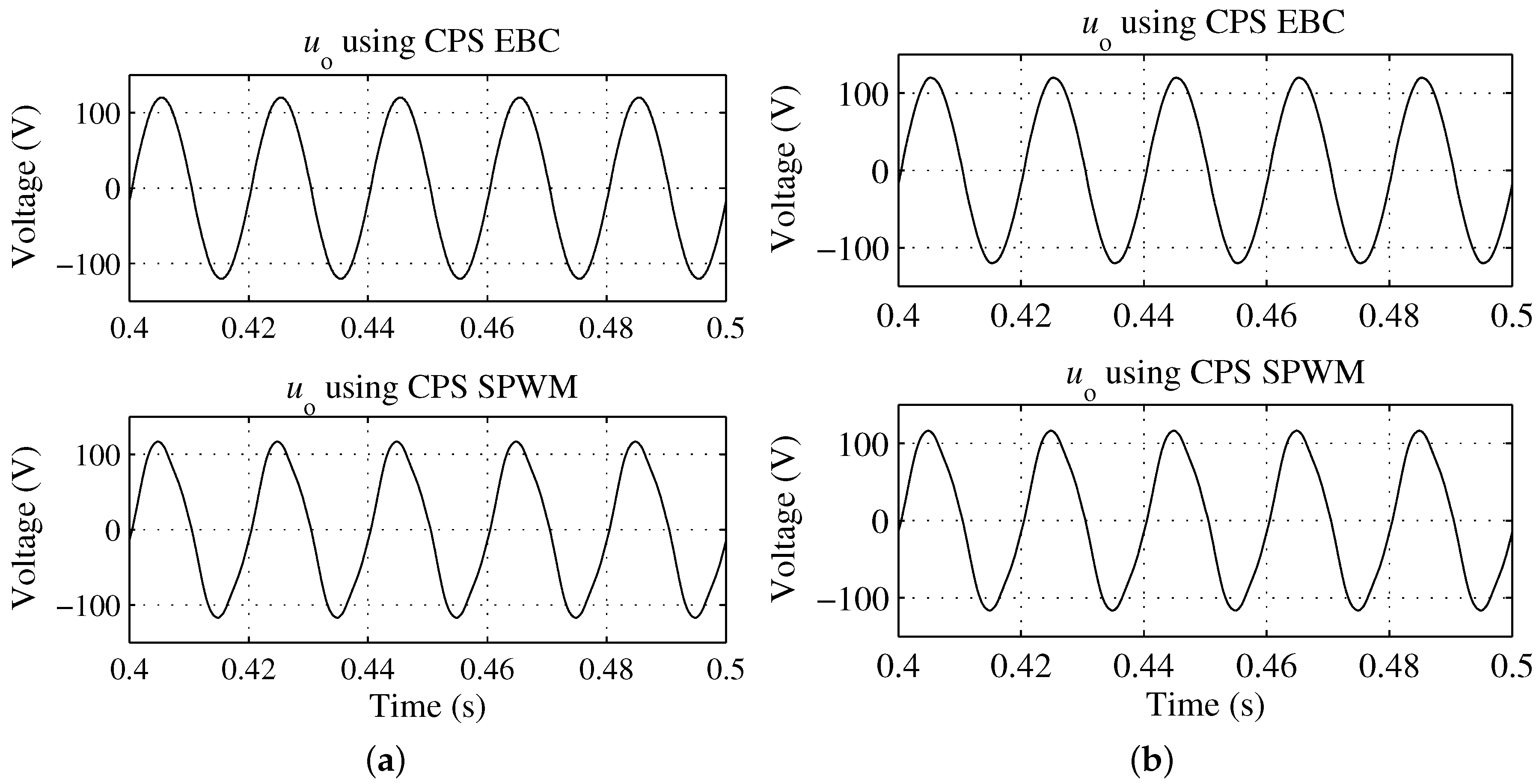
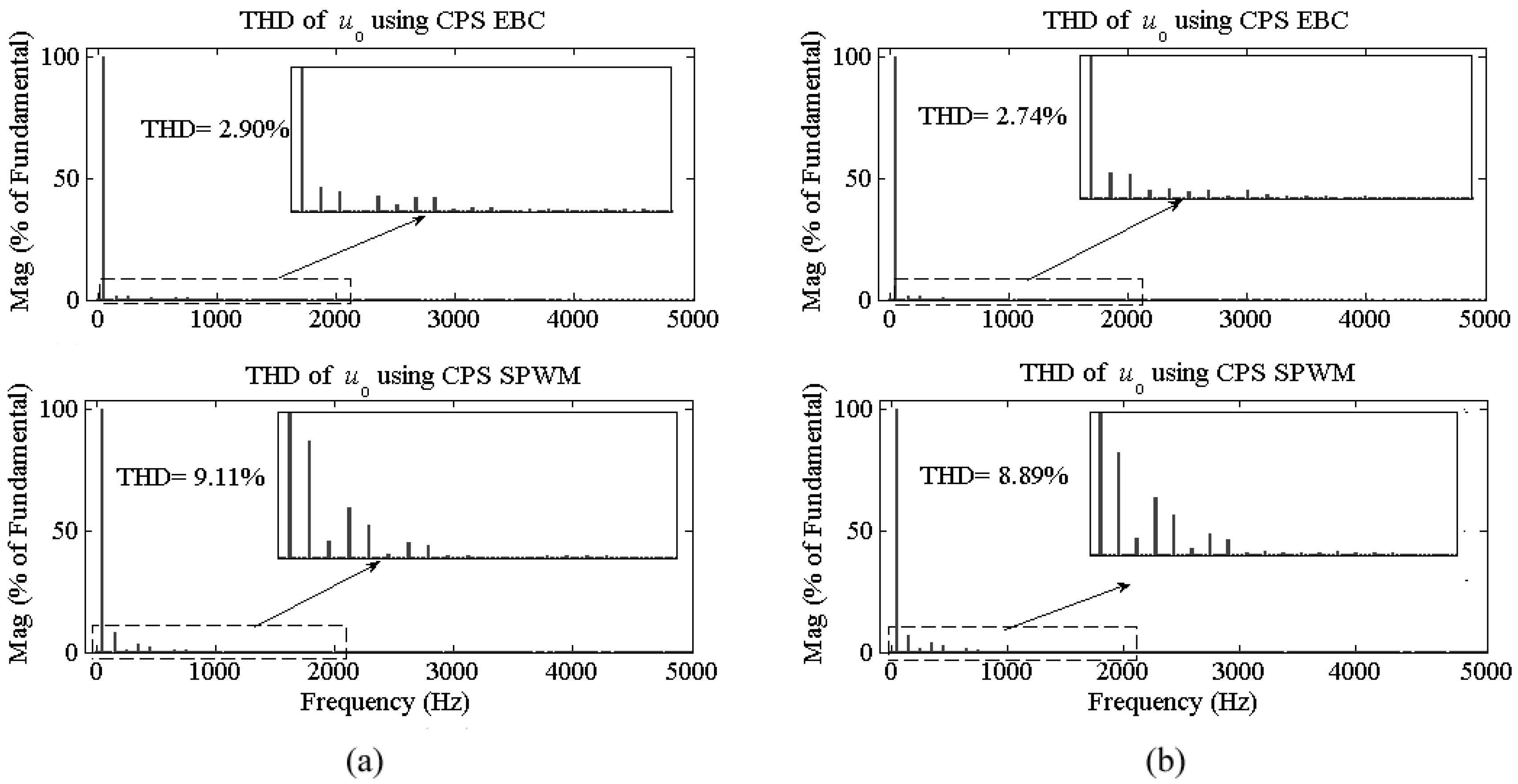
4.3. The Suppression Ability of the CPS EBC against Interferences in DC Sources

To evaluate the ability of the CPS EBC to suppress the fluctuations of DC sources, DC sources ( u 1 , u 2 , , u n ) are designed by DC voltage mixed with low frequency interferences. The simulation and experimental results are demonstrated in Figure 12, Figure 13, Figure 14 and Figure 15.
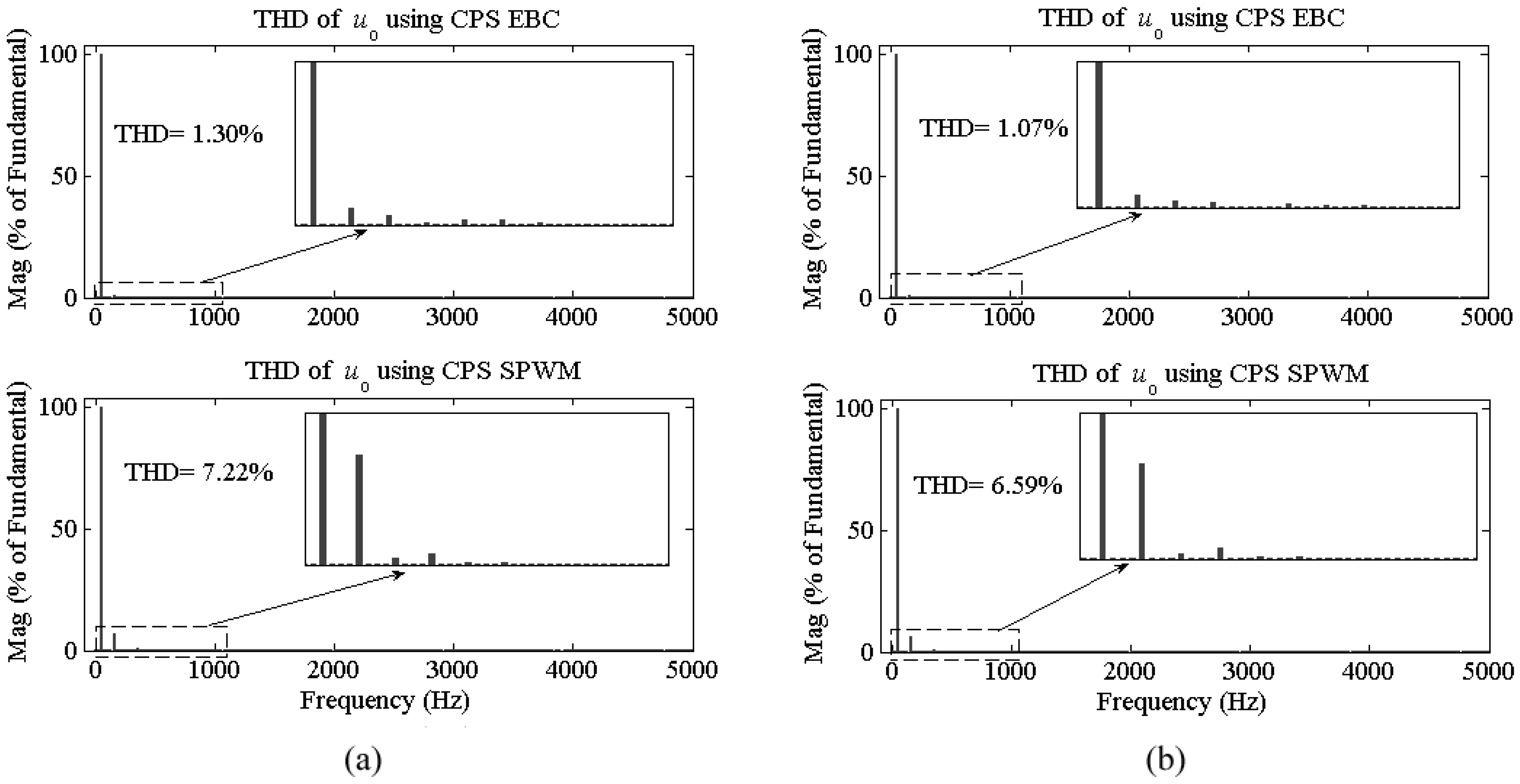
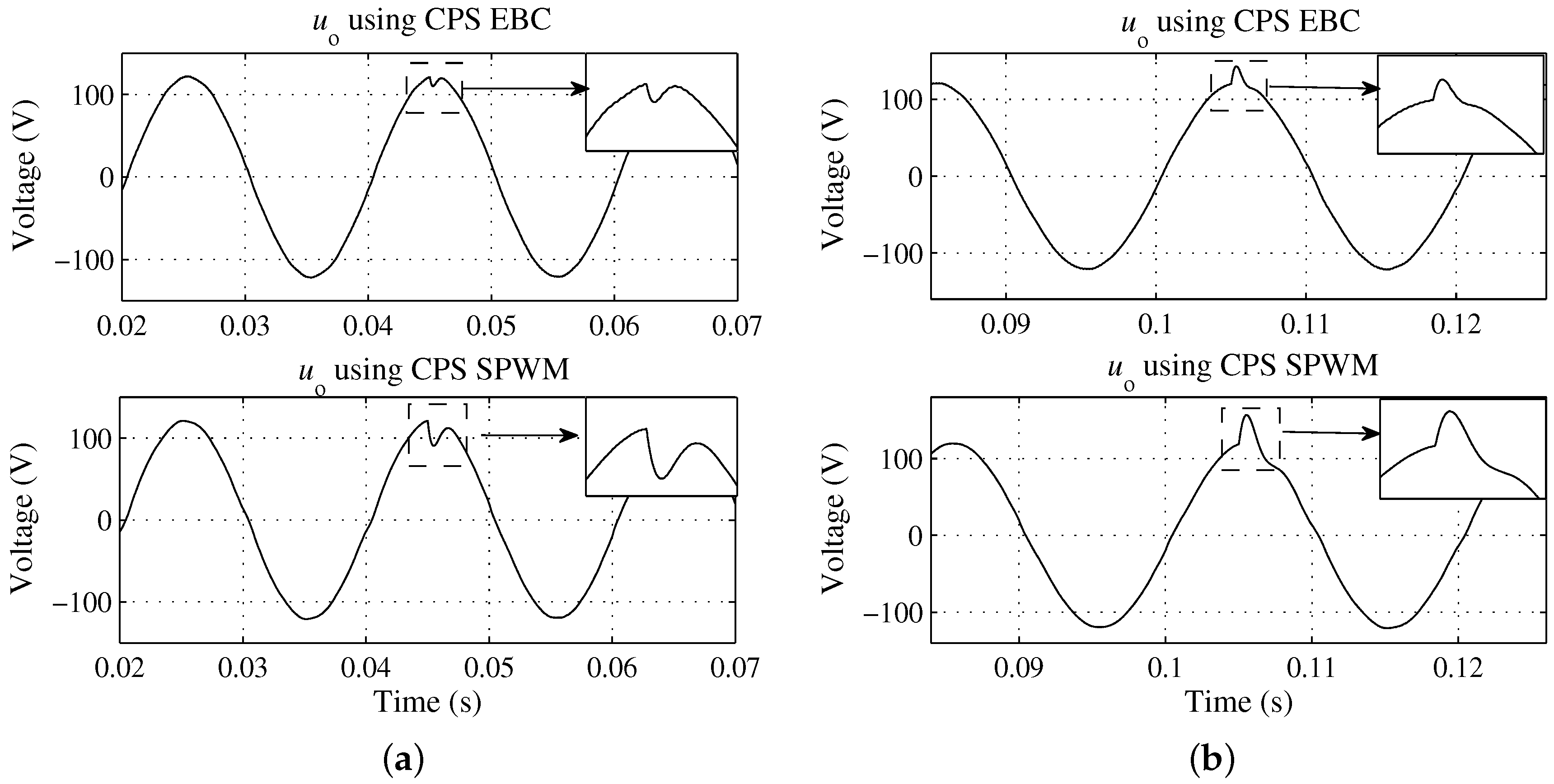
Figure 12a shows the simulation results under unbalance DC voltages (a ripple with a frequency 100 Hz and an amplitude 16 V is added in u 1 ). The comparison results demonstrate that u o using CPS SPWM is not a ideal sine wave but with distortions. The FFT analysis in Figure 13a shows low order harmonic voltages are contained in u o . In comparison, u o using the CPS EBC is kept as a ideal sine wave. No low order harmonic voltages are brought into u o , as shown in Figure 13a. Similarly, under the DC voltages mixed with low frequency ripples ( 100 Hz ripples with an amplitude 8 V are added in u 1 and u 2 , respectively). The comparison results in Figure 12b illustrate that u o using the CPS SPWM distorts due to the low order harmonic voltages. However, u o using the CPS EBC, is kept as a ideal sine wave. This can also be observed from the comparison of the FFT analysis in Figure 13b. Figure 14 and Figure 15 display the experimental results using the CPS EBC and the CPS SPWM under the cases of unbalanced DC voltage and DC voltage with fluctuations. From the comparisons, it can be observed that the experimental results are consistent with the simulation results in Figure 12. All the comparison results of the THD of u o under the cases of unbalance DC voltages and DC voltages containing low frequency ripples are summarized in Table 3. The figures and tables verify that the CPS EBC has strong inhibitions against fluctuations of DC sources.

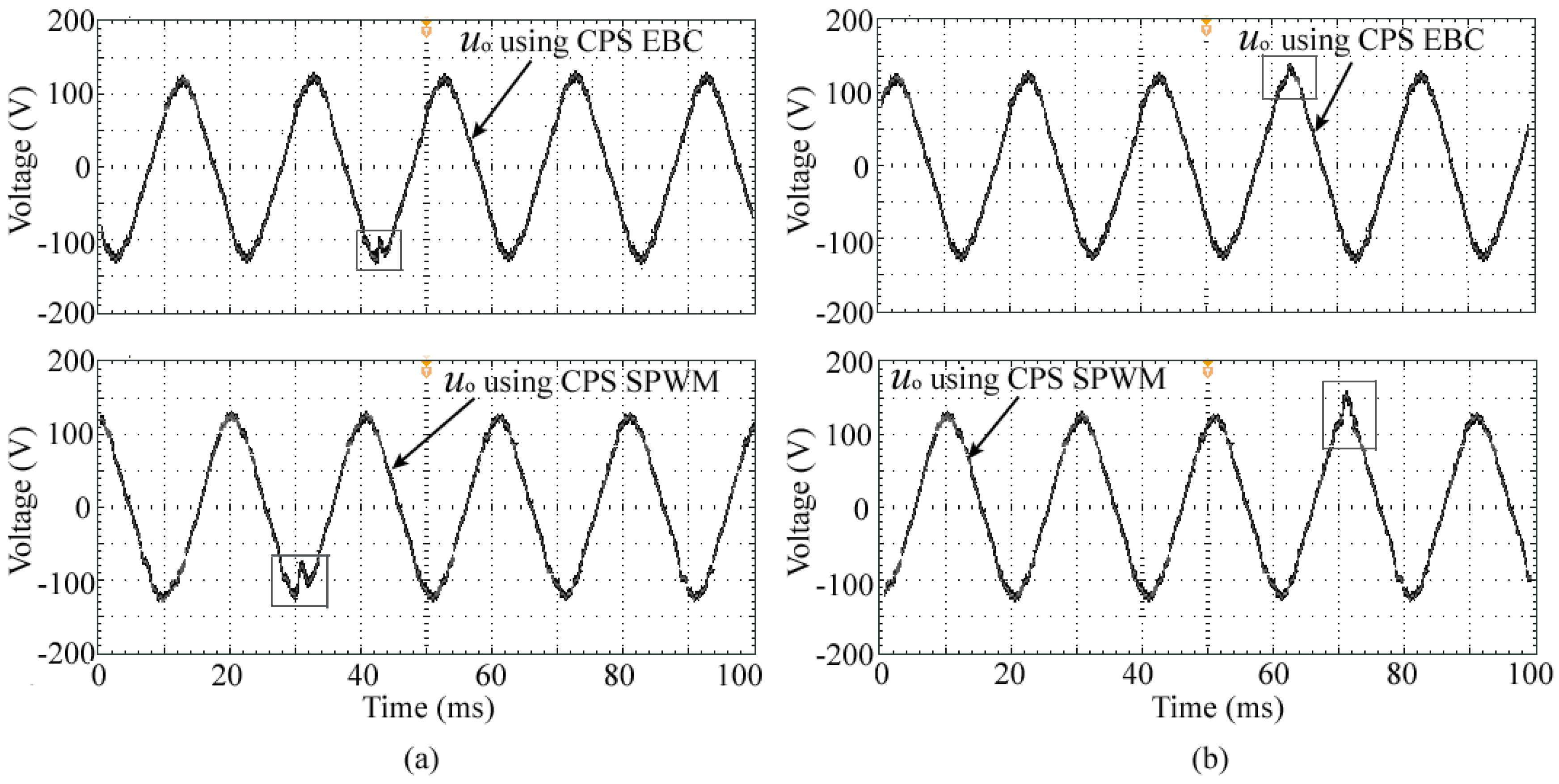
4.4. The Dynamic Responses of CPS EBC to Load Variations

To evaluate the dynamic performances of the proposed CPS EBC, the responses to variations in the load of the converter using the CPS EBC is compared with that of the CPS SPWM. Figure 16 and Figure 17 demonstrate the comparison results.
In the simulation and experiment, the load steps from 50 Ω 25 Ω at t = 0.045 s and 25 Ω 50 Ω at t = 0.105 s . The comparison results of the voltage shoot Δ u o and the settling time t settling of the dynamic responses to the load variations are summarized in Table 4. From the figures and table, it can be observed that, under the load variation, Δ u o and t settling are significantly reduced by using the proposed CPS EBC. For instance, under the load variation from 50 Ω to 25 Ω , the simulation results of Δ u o is reduced from 26 V (using CPS SPWM) to 10 V (using CPS EBC) and t settling is reduced from 1.9 ms (using CPS SPWM) to 0.9 ms (using CPS EBC).
Thus, the improved dynamic responses to load variations of the CPS EBC method are verified from the above simulation and experimental results.

5. Conclusions

The CPS EBC method has been proposed and implemented for controlling the cascaded half-bridge multilevel inverters for standalone solar PV applications. It is composed by n similar but independent EBC controllers. DC sources mixed with fluctuations are designed to simulate the DC voltage supplied by the solar PV arrays. Simulation and experimental results demonstrate that, by shifting the phase of the clock pulse of each cascaded half-bridge, staircase-like voltage waveforms are obtained. Under the cases of unbalance DC voltage, DC voltages with low frequency ripples and load variations, the comparison results between the CPS EBC and the CPS SPWM method reveal that the CPS EBC produces a superior ability in suppressing the fluctuations in DC voltages and improved dynamic performances under load variations, in terms of shorter settling time and smaller voltage shoots. Thus, the distortions of the output voltage of the solar PV systems, due to the power imbalance, the DC supply with fluctuations are avoided. Meanwhile the dynamic responses to load variations are improved. These results illustrate that the CPS EBC method is more suitable than the CPS SPWM to control multilevel inverters for standalone solar PV applications.

Acknowledgments

The work is supported by Guangdong Innovative Research Team Program (No. 201001 N0104744201) and in part by the State Key Program of National Natural Science of China under Grant 51437006.

Author Contributions

All the authors conceived and designed the study. Lei Wang performed the simulation and the experiment and wrote the manuscript with guidance from Qinghua Wu and Wenhu Tang.

Conflicts of Interest

The authors declare no conflict of interest.

Abbreviations

The following abbreviations are used in this manuscript:
CPSClock phase-shifting
EBCEnergy balance control
PVPhotovoltaic
CHBCascaded H-bridge
R-LResistance-inductance
PWMPulse-width Modulation
SV-PWMSpace vector PWM
SMCSliding-mode control
CPS SPWMCarrier phase shifted-sinusoidal pulse width modulation
MPPTMaximum power point tracking
THDTotal harmonic distortion
FFTFast fourier transform

References

  1. Chye, M.S.; Tan, Y.C.; Soo, J.A.; Ong, S.L.; Azmi, S.A.; Leong, J.H. Standalone solar power generation using 3-phase multilevel inverter with simpler basic unit cells. In Proceedings of the 2016 3rd International Conference on Electronic Design (ICED), Phuket, Thailand, 11–12 August 2016; pp. 531–536. [Google Scholar] [CrossRef]
  2. Duman, T.; Marti, S.; Moonem, M.A.; Krishnaswami, H. A modular multilevel converter with power mismatch control for grid-connected photovoltaic systems. Energies 2017, 10, 698. [Google Scholar] [CrossRef]
  3. Villanueva, E.; Correa, P.; Rodriguez, J.; Pacas, M. Control of a single-phase cascaded H-bridge multilevel inverter for grid-connected photovoltaic systems. IEEE Trans. Ind. Electron. 2009, 56, 4399–4406. [Google Scholar] [CrossRef]
  4. Ebrahim, B.; Somayeh, A.; Laali, S. A new general topology for cascaded multilevel inverters with reduced number of components based on developed H-Bridge. IEEE Trans. Ind. Electron. Convers. 2014, 61, 3932–3939. [Google Scholar] [CrossRef]
  5. Khajehoddin, S.A.; Bakhshai, A.; Jain, P.K. A simple voltage balancing scheme for m-level diode-clamped multilevel converters based on a generalized current flow model. IEEE Trans. Power Electron. 2008, 23, 2248–2259. [Google Scholar] [CrossRef]
  6. Nami, A.; Zare, F.; Ledwich, G.; Ghosh, A.; Blaabjerg, F. Comparison between symmetrical and asymmetrical single phase multilevel inverter with diode-clamped topology. In Proceedings of the 2008 IEEE Power Electronics Specialists Conference (PESC), Rhodes, Greece, 15–19 June 2008; pp. 2921–2926. [Google Scholar] [CrossRef]
  7. Sepahvand, H.; Corzine, K.A.; Ferdowsi, M.; Khazraei, M. Active capacitor voltage balancing in single-phase flying-capacitor multilevel power converters. IEEE Trans. Ind. Electron. 2012, 59, 769–778. [Google Scholar] [CrossRef]
  8. Khoshkbar-Sadigh, A.; Dargabi, V.; Corzine, K. New flying-capacitor-based multilevel converter with optimized number of switches and capacitors for renewable energy integration. IEEE Trans. Energy Convers. 2016, 31, 846–859. [Google Scholar] [CrossRef]
  9. Babaei, E.; Hosseini, S.H. New cascaded multilevel inverter topology with minimum number of switches. Energy Convers. Manag. 2009, 50, 2761–2767. [Google Scholar] [CrossRef]
  10. Alishah, R.S.; Nazarpour, D.; Hosseini, S.H. Novel topologies for symmetric, asymmetric, and cascade switched-diode mutilevel converter with minimum number of power electronic components. IEEE Trans. Ind. Electron. 2014, 61, 5300–5310. [Google Scholar] [CrossRef]
  11. Alishah, R.S.; Nazarpour, D. New hybrid structure for multilevel inverter with fewer number of components for high-voltage levels. IET Power Electron. 2013, 7, 96–104. [Google Scholar] [CrossRef]
  12. Wang, L.; Wu, Q.H.; Tang, W.H. Novel cascaded switched-diode multilevel inverter for renewable energy integration. IEEE Trans. Energy Convers. 2017, PP, 1–1. [Google Scholar] [CrossRef]
  13. McGrath, B.P.; Holmes, D.G. Multicarrier PWM strategies for multilevel inverters. IEEE Trans. Ind. Electron. 2002, 49, 858–867. [Google Scholar] [CrossRef]
  14. Zhou, F.; Luo, A.; Li, Y.; Xu, Q.; He, Z.; Guerrero, J.M. Double-carrier phase-disposition pulse width modulation method for modular multilevel converters. Energies 2017, 10, 581. [Google Scholar] [CrossRef]
  15. Tang, X.; Zhang, J.; Liu, Z.; Zhang, M. A switching frequency optimized space vector pulse width modulation (SVPWM) scheme for cascaded multilevel inverters. Energies 2017, 10, 725. [Google Scholar] [CrossRef]
  16. Shukla, A.; Ghosh, A.; Joshi, A. Hysteresis modulation of multilevel inverters. IEEE Trans. Power Electron. 2011, 26, 1396–1409. [Google Scholar] [CrossRef]
  17. Gupta, R.; Ghosh, A.; Joshi, A. Multi-band hysteresis modulation and switching characterization for sliding mode controlled cascaded multilevel inverter. IEEE Trans. Ind. Electron. 2010, 57, 2344–2353. [Google Scholar] [CrossRef]
  18. Cecati, C.; Ciancetta, F.; Siano, P. A multilevel inverter for photovoltaic systems with fuzzy logic control. IEEE Trans. Ind. Electron. 2010, 57, 4115–4125. [Google Scholar] [CrossRef]
  19. Yu, Y.F.; Konstantinou, G.; Hredzak, B.; Vassilios, G.A. Power balance of cascaded H-bridge multilevel converters for large-scale photovoltaic integration. IEEE Trans. Power Electron. 2016, 31, 292–303. [Google Scholar] [CrossRef]
  20. Christopher, D.T.; Yu, Y.F.; Konstantinou, G.; Vassilios, G.A. Cascaded H-bridge multilevel PV topology for alleviation of per-phase power imbalances and reduction of second harmonic voltage ripple. IEEE Trans. Power Electron. 2016, 31, 5574–5586. [Google Scholar] [CrossRef]
  21. Yu, Y.F.; Konstantinou, G.; Hredzak, B.; Vassilios, G.A. Predictive control of cascaded H-bridge converters under unbalanced power generation. IEEE Trans. Power Electron. 2017, 64, 292–303. [Google Scholar] [CrossRef]
  22. Chavarria, J.; Biel, D.; Guinjoan, F.; Meza, C.; Negroni, J. Energybalance control of PV cascaded multilevel grid-connected converters under level-shifted and phase-shifted PWMs. IEEE Trans. Ind. Electron. 2013, 60, 98–111. [Google Scholar] [CrossRef]
  23. Rodriguez, J.; Lai, J.S.; Peng, F.Z. Mutilevel inverters: A survey of topologies, controls, and application. IEEE Trans. Ind. Electron. 2002, 49, 724–738. [Google Scholar] [CrossRef]
  24. Wang, L.; Wu, Q.H.; Tao, Y.K.; Tang, W.H. Switching control of buck converter based on energy conservation principle. IEEE Trans. Control Syst. Technol. 2016, 24, 1779–1787. [Google Scholar] [CrossRef]
  25. Alexander, A.; Thathan, M. Modelling and analysis of modular multilevel converter for solar photovoltaic applications to improve power quality. IET Renew. Power Gener. 2015, 9, 78–88. [Google Scholar] [CrossRef]
Figure 1. Standalone solar PV system with a cascaded half-bridge multilevel inverter.
Energies 10 01805 g001
Figure 2. The structure of the topology leaving out the details of the second stage.
Energies 10 01805 g002
Figure 3. The structure of the CPS EBC method for the topology leaving out the details of the second stage.
Energies 10 01805 g003
Figure 4. The hardware and interface of the experimental prototype.
Energies 10 01805 g004
Figure 5. Gate signals of the five-level simulation prototype. (a) The gates of the first stage; and (b) The gates of the second stage.
Energies 10 01805 g005
Figure 6. The simulation results of the five-level prototype. (a) The output voltage u g and current i g of the first stage; (b) The output voltage u o and current i o of the second stage.
Energies 10 01805 g006
Figure 7. The fast fourier transform (FFT) analysis result of u AB . (a) The five-level simulation prototype; and (b) The nine-level simulation prototype.
Energies 10 01805 g007
Figure 8. The simulation results of the nine-level prototype. (a) The output voltage u g and current i g of the first stage; and (b) The output voltage u o and current i o of the second stage.
Energies 10 01805 g008
Figure 9. The experimental results of the operation of the five-level prototype using CPS EBC. (a) The output voltage u g of the first stage (figure top); The current i g and i o (figure bottom); and (b) The stepped voltage u AB (figure top); The output voltage u o (figure bottom).
Energies 10 01805 g009
Figure 10. The FFT analysis result of the experimental prototype. (a) The stepped voltage u AB ; and (b) The output voltage u o .
Energies 10 01805 g010
Figure 11. The results of the five-level prototype under the case of power imbalance ( u 1 = 65 V and u 2 = 80 V ). (a) Simulation results; and (b) Experimental results.
Energies 10 01805 g011
Figure 12. The simulation results of the five-level prototype under the case of unbalance DC voltages and DC voltages with fluctuations. (a) DC voltage u 1 contains a ripple with a frequency of 100 Hz and an amplitude of 16 V ; and (b) DC voltage of each cascaded unit contains a frequency of 100 Hz and an amplitude of 8 V .
Energies 10 01805 g012
Figure 13. The comparison of the THD of the five-level simulation prototype under the case of DC voltages with fluctuations. (a) DC voltage u 1 contains a ripple with a frequency of 100 Hz and an amplitude of 16 V ; and (b) DC voltage of each cascaded unit contains a frequency of 100 Hz and an amplitude of 8 V .
Energies 10 01805 g013
Figure 14. The experimental results of the five-level prototype under the case of DC voltages with fluctuations. (a) DC voltage u 1 contains a ripple with a frequency of 100 Hz and an amplitude of 16 V ; and (b) DC voltage of each cascaded unit contains a frequency of 100 Hz and an amplitude of 8 V .
Energies 10 01805 g014
Figure 15. The comparison of the THD of the five-level experimental prototype under the case of DC voltages with fluctuations. (a) DC voltage u 1 contains a ripple with a frequency of 100 Hz and an amplitude of 16 V ; and (b) DC voltage of each cascaded unit contains a frequency of 100 Hz and an amplitude of 8 V .
Energies 10 01805 g015
Figure 16. The simulation results of the five-level prototype under cases of load steps. (a) load steps as 50 Ω 25 Ω ; and (b) load steps as 25 Ω 50 Ω .
Energies 10 01805 g016
Figure 17. The experiment results of the five-level prototype under cases of load steps. (a) load steps as 50 Ω 25 Ω ; and (b) load steps as 25 Ω 50 Ω .
Energies 10 01805 g017
Table 1. Values of u g under different switch states of the first stage.
StateSwitches States u g
S 11 S 12 S 21 S 22 S ( n 1 ) 1 S ( n 1 ) 2 S n 1 S n 2
1 off on off on off on off on 0
2 on off off on off on off on u 1
3 off on on off off on off on u 2
n off on off on off on on off u n
n + 1 on off on off off on off on u 1 + u 2
2 n on off on off on off on off i = 1 n u i
Table 2. Values of u o under different switch states of the second stage.
StateSwitches States u o Condition
S 1 S 2 S 3 S 4
1 on off off on u g u ref > 0
2 off on on off u g u ref < 0
Table 3. Simulation and Experimental results under DC voltages with fluctuation.
CasesSimulationExperiment
CPS EBCCPS SPWMCPS EBCCPS SPWM
THD (%)Unbalance DC sources1.307.222.909.11
DC sources with fluctuation1.076.592.748.89
Table 4. Simulation and Experimental results under load variations.
R ( Ω ) CPS EBCCPS SPWM
Δ u o ( V ) t settling ( ms ) Δ u o ( V ) t settling ( ms )
Simulation50 → 25 10 0.9 26 1.9
25 → 50181.2322
Experiment50 → 25−161.2−322.2
25→ 50181.4362.3

