Article

A Digital Hysteresis Current Control for Half-Bridge Inverters with Constrained Switching Frequency

Internet of Energy Laboratory, Department of Technology Management for Innovation, The University of Tokyo, Tokyo 113-8656, Japan
*
Author to whom correspondence should be addressed.
Energies 2017, 10(10), 1610; https://doi.org/10.3390/en10101610
Submission received: 7 September 2017 / Revised: 9 October 2017 / Accepted: 12 October 2017 / Published: 14 October 2017
(This article belongs to the Special Issue Power Electronics and Power Quality)

Abstract

:
This paper proposes a new robustly adaptive hysteresis current digital control algorithm for half-bridge inverters, which plays an important role in electric power, and in various applications in electronic systems. The proposed control algorithm is assumed to be implemented on a high-speed Field Programmable Gate Array (FPGA) circuit, using measured data with high sampling frequency. The hysteresis current band is computed in each switching modulation period based on both the current error and the negative half switching period during the previous modulation period, in addition to the conventionally used voltages measured at computation instants. The proposed control algorithm is derived by solving the optimization problem—where the switching frequency is always constrained at below the desired constant frequency—which is not guaranteed by the conventional method. The optimization problem also keeps the output current stable around the reference, and minimizes power loss. Simulation results show good performances of the proposed algorithm compared with the conventional one.

1. Introduction

Nowadays, inverters and their controllers play an important role in the enabling of a wider proliferation of renewable energy generation [1,2], the realization of new grid concepts with high efficiency [3,4], and various applications in electronic systems [5,6]. Among various current control techniques developed over last few decades, there are three major classes of control scheme: sine-triangle Pulse Width Modulation (PWM), predictive dead-beat, and hysteresis current control. While the asynchronous sine-triangle PWM is a popular technique to modulate current error, it requires a PI (Proportional-Integral) regulator and often results in unavoidable delays. The predictive dead-beat control technique tends to give good performance in terms of response and accuracy. However, this technique is highly dependent on the accuracy of the predictive model and is complicated to implement [7]. Hysteresis current control, on the other hand, is simpler to implement and does not have such drawbacks. It has a fast dynamic response, and does not require any information about the system parameters, which enhances its robustness [5,8]. For this reason, it finds applications in a large variety of switching inverters.
The basic implementation of hysteresis current control is based on the switching signal that is derived by comparing the actual current and the reference current so that the current error is kept within the tolerance current band. In classical hysteresis current controllers, the hysteresis current band is normally fixed to a certain value, which makes the switching frequency vary in order to contain the current ripple within the band. This leads to unwanted heavy interference among the phases in the three-phase system [9]. In order to overcome this problem, an adaptive hysteresis current control technique has been developed and used in many applications [10,11,12]. In this technique, the hysteresis current band is not fixed, but controlled adaptively in each switching modulation period, and based on the measured output voltage values and the desired constant switching frequency [13].
Digital hysteresis current control usually requires a sufficiently high sampling frequency to control the switch devices with accurate switching time [14,15]. The ripple current varies during each switching modulation at a very fast rate, which is inversely proportional to the output inductance and proportional to the difference between the dc and output voltages. Because, during the sampling interval, the hysteresis current band could not be observed until the arrival of the next data sample, the low sampling frequency may lead to a large ripple current overshoot from the hysteresis current band. A high sampling frequency at the MHz level seems to be quite high for conventional Digital Signal Processors (DSP) and microcontrollers, which are employed in most power electronic applications at present. Additionally, such a high sampling frequency is beyond the scope of the Field Programmable Gate Array (FPGA) circuit, which has a high-speed clock and is becoming more and more popular in inverter control [16,17,18].
In many applications, the high switching frequency has several advantages including lower current ripple, faster transient response, and effective size reduction for the inverter circuit [19,20,21]. In some cases, the switching devices are operated near the highest possible switching frequency, for example when the controller is redesigned for an existing device, or in order to reduce the price of the inverters. For instance, when a motor is accelerated from a standstill to rated speed, an inverter is usually designed to operate near its highest possible switching frequency in order to achieve a low current distortion [22]. In these cases, if the switching devices are forced to change their on-off states at a frequency beyond their limit, especially under the influence of noise, short-circuit fault can occur and may lead to breakage of the switching device [23]. Therefore, it is important to properly control the hysteresis current band so that the frequency of the switching device does not exceed its highest possible switching frequency. However, the switching frequency fluctuation controlled by the conventional method is not guaranteed to never exceed this limit, especially with noise. The conventional method of computing a hysteresis current band uses only the measured voltage values at the instant when the switches start a new modulation period [13,24]. The present study proposes a new digital hysteresis current control algorithm that takes the feedback information from the preceding modulation period into account, keeping the switching frequency constant and always below the highest possible switching frequency of the switching device, even when noise is present. The controller is assumed to be using an FPGA while the sampling interval is at the MHz level.
This paper is organized as follows. Section 2 presents a conventional method of using the fixed band hysteresis current. In Section 3, a conventional adaptive hysteresis current control is described and its disadvantages are explained. Then, a new robustly-adaptive hysteresis current control algorithm is proposed in Section 4. In Section 5, the simulation results are shown to demonstrate that the proposed method has better performance than the conventional method. Conclusions are given in Section 6.

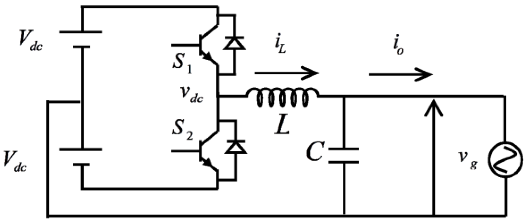
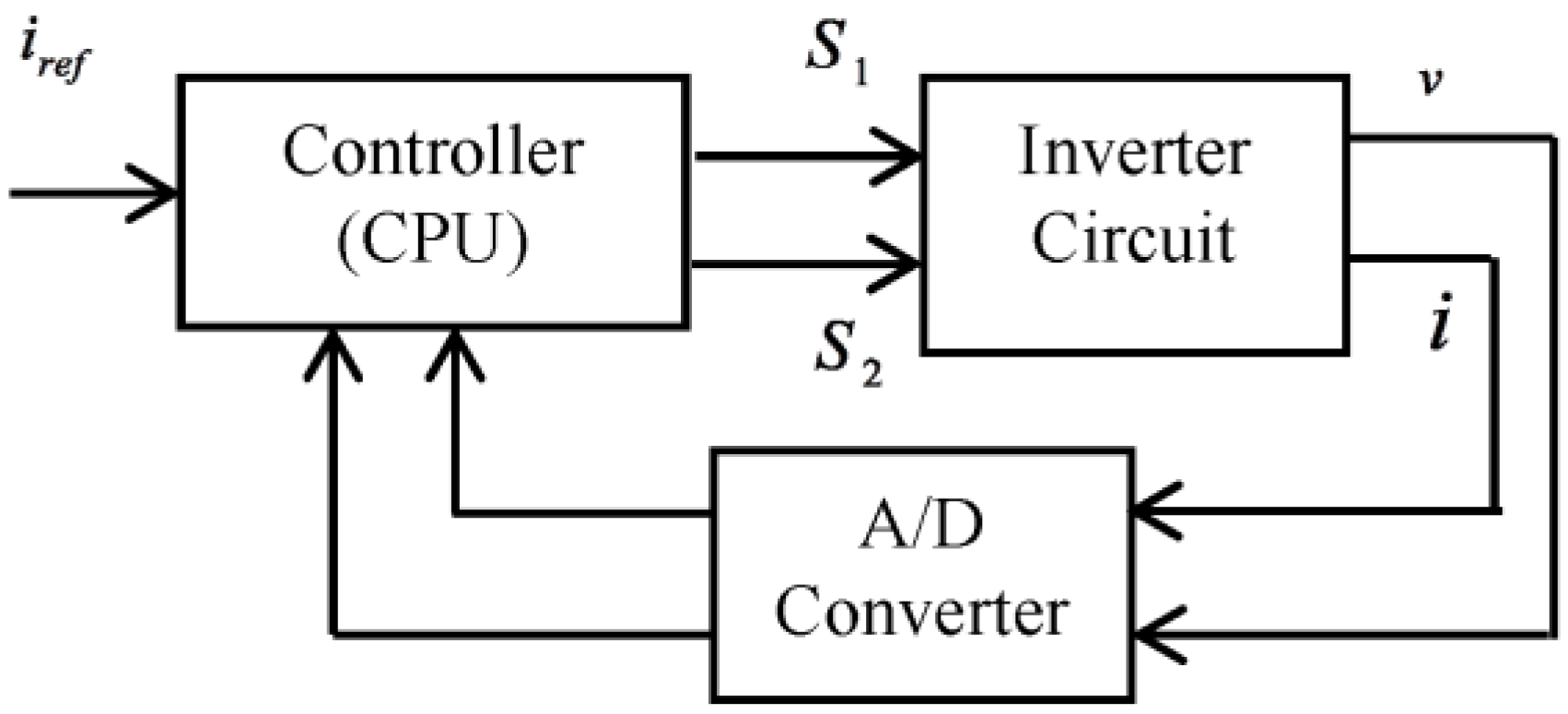
2. Classical Fixed Band Hysteresis Current Control

Consider a single-phase half-bridge inverter circuit, where the output is connected to a grid ac voltage v g as in Figure 1. The dc voltage is supplied by two constant and balanced dc sources, each of which has a value of V d c . Parameters L , C , and R present the output inductance, current ripple filter, and load respectively. The inverter output current i L is controlled by the switching devices S 1 and S 2 to track a given reference current i r e f . The ripple component of the output current i L is filtered by the current ripple filter, and the grid current i o is derived without a ripple component.
Figure 2 shows the structure of the digital control system. The measured output voltages, and currents are sampled by analog/digital converters, and used for computing on/off pulses of switches S 1 and S 2 . The states of the switches and the corresponding inputs and outputs of the inverter are shown in Table 1.
In the classical fixed band hysteresis current control, the tolerance current band is fixed to a certain value Δ i b [25]. While the measured output current i L is between the upper and lower limits, no switching occurs. When the measured output current crosses above the upper limit of the hysteresis band ( i r e f + Δ i b ) , the switch S 1 is turned off, the switch S 2 is turned on and the current starts to decay. In contrast, when the measured current crosses below the lower limit of the hysteresis band ( i r e f Δ i b ) , the switch S 1 is turned on, the switch S 2 is turned off and the current starts to increase (Figure 3).
The hysteresis current band value is directly proportional to the current ripple and inversely proportional to the switching frequency. Thus, increasing the value of the hysteresis current band will increase the current ripple while a decrease in the band will increase the switching losses. In analog controllers, the current ripple is always kept exactly within the hysteresis band. However, in digital controllers, the hysteresis control is shown to be effective only if the current band is chosen to satisfy the following condition [5]:
Δ i b > max ( d i r e f d t ) 1 f s p ,
where f s p is the sampling frequency. The maximum switching frequency f s w _ max should be smaller than half the sampling frequency f s p , i.e.,:
f s w _ max 1 2 f s p .

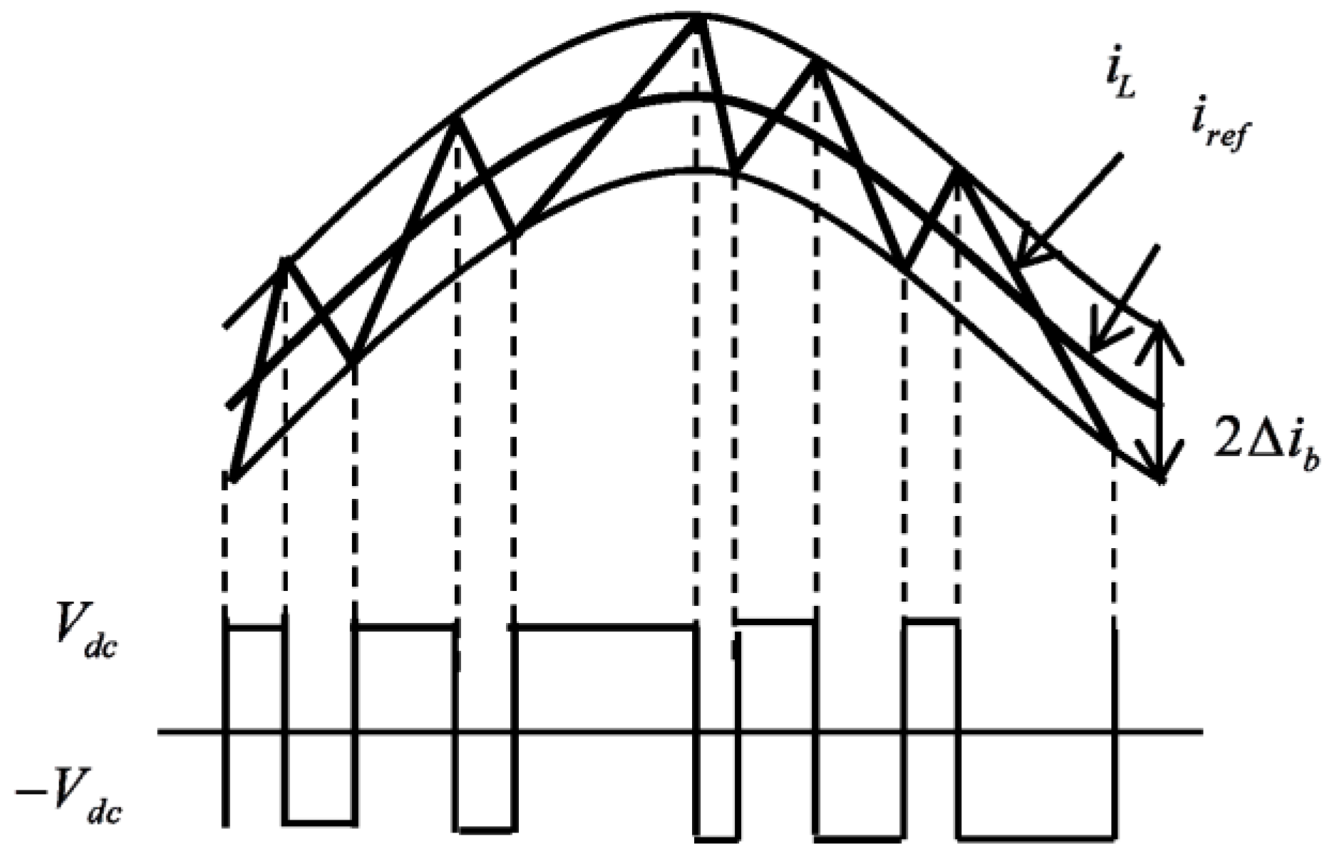
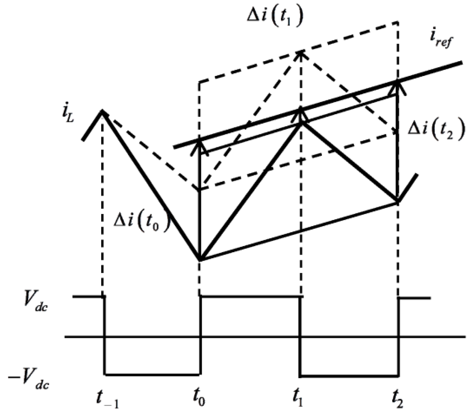
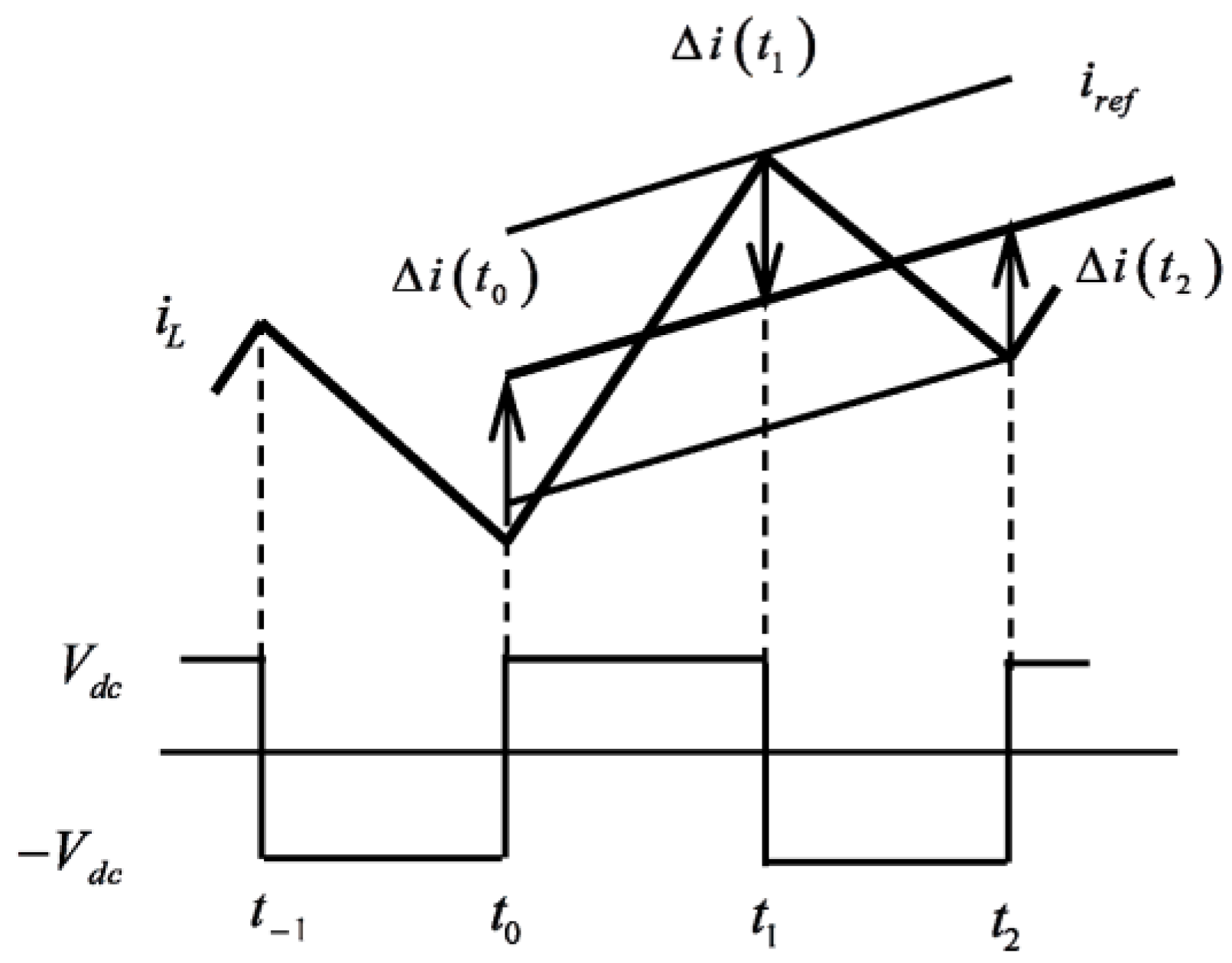
3. Conventional Adaptive Hysteresis Current Control

3.1. Algorithm of the Convention Adaptive Hysteresis Current Control

The above mentioned fixed band hysteresis control has many advantages: its simplicity, its fast and stable response, and its independence from system parameters. However, a disadvantage is that the switching frequency needs to vary in order to keep the peak-to-peak current ripple controlled at all points on the fundamental frequency wave [10]. In order to solve this problem, the adaptive hysteresis current control technique has been presented in the literature [7,26]. In this technique, the hysteresis current band is not fixed, but controlled adaptively in each switching modulation period, based on the measured output voltage values and the desired constant switching frequency. The adaptive hysteresis current control is employed as shown below.
Define the current error Δ i ( t ) as:
Δ i ( t ) = i L ( t ) i r e f ( t ) ,
where i L ( t ) , and i r e f ( t ) are the inverter output and the reference currents, respectively, at instant t . Consider the instant t 0 , when the output current i L tends to cross the lower hysteresis band, and the switch S 1 is switched on. The current error at t 0 is Δ i ( t 0 ) (Figure 4). Assume that the switch S 1 is switched on during [ t 0 , t 1 ) , and is switched off during [ t 1 , t 2 ) intervals. These intervals are called positive and negative half switching periods respectively.
The output current dynamic equation can be written as:
d i L ( t ) d t = v d c ( t ) v g ( t ) L
for t 0 t t 2 , where v g is the instantaneous grid voltage, L is the output inductance, and v d c ( t ) is the inverter dc voltage, and can be elaborated as:
v d c ( t ) = { V d c i f S 1 i s O n V d c i f S 1 i s O f f .
Define the output current slopes in the on and off periods by I ˙ o n , and I ˙ o f f respectively. Assuming that the output voltage is slowly varying during the switching modulation period [ t 0 , t 2 ] , the output current slopes (4) can be expressed as:
I ˙ o n = d i L ( t ) d t = V d c v g ( t 0 ) L
for t [ t 0 , t 1 ) , and:
I ˙ o f f d i L ( t ) d t = V d c v g ( t 0 ) L
for t [ t 1 , t 2 ) .
The current errors in the positive and negative half switching periods are given as:
Δ i ( t 1 ) = i L ( t 1 ) i r e f ( t 1 ) = i r e f ( t 0 ) +   Δ i ( t 0 ) +   I ˙ o n T o n i r e f ( t 1 )   ,
Δ i ( t 2 ) = i L ( t 2 ) i r e f ( t 2 ) = i r e f ( t 0 ) +   Δ i ( t 0 ) + ( I ˙ o n T o n +   I ˙ o f f T o f f )   i r e f ( t 2 ) .
where T o n and T o f f are the on and off periods of switch S 1 , given as:
T o n = t 1 t 0
T o f f = t 2 t 1
The reference current i r e f ( t ) is slowly varying during the modulation period, such that it can be approximated as:
i r e f ( t 1 ) = i r e f ( t 0 ) + I ˙ r e f ( t 0 ) T o n ,
i r e f ( t 2 ) = i r e f ( t 0 ) + I ˙ r e f ( t 0 ) ( T o n + T o f f ) ,
where:
I ˙ r e f ( t 0 ) = d i r e f ( t ) d t | t = t 0
By substituting Equations (12) and (13) into Equations (8) and (9), one can write the current errors Δ i ( t 1 ) , and Δ i ( t 2 ) as:
Δ i ( t 1 ) = Δ i ( t 0 ) + I ˙ o n T o n
Δ i ( t 2 )   =     Δ i ( t 0 ) + I ˙ o n T o n + I ˙ o f f T o f f = Δ i ( t 1 ) + I ˙ o f f T o f f
where I ˙ o n and I ˙ o f f are the current error slopes in positive and negative half switching periods, given as:
I ˙ o n = I ˙ o n I ˙ r e f ( t 0 ) = V d c v g ( t 0 ) L I ˙ r e f ( t 0 ) ,
I ˙ o f f = I ˙ o f f I ˙ r e f ( t 0 ) = V d c v g ( t 0 ) L I ˙ r e f ( t 0 )
Let f s w be the desired constant switching frequency. In the conventional adaptive hysteresis current control method, the hysteresis current band Δ i b ( t 0 ) is derived by using the following conditions:
Δ i ( t 1 )   Δ i ( t 0 )   = 2 Δ i b ( t 0 )
Δ i ( t 2 )   Δ i ( t 1 )   = 2 Δ i b ( t 0 ) ,
T o n + T o f f = T s w ,
where T s w = 1 / f s w is the desired constant switching period. Substituting Equations (19)–(21) into Equations (15) and (16), we can derive the hysteresis current band as:
Δ i b ( t 0 ) = 1 2 I ˙ o n I ˙ o f f I ˙ o f f I ˙ o n T s w
By substituting Equations (17) and (18) into Equation (22), the hysteresis band in Equation (22) can also be written in the form of [26] :
Δ i b ( t 0 ) = V d c T s w 4 L ( 1 m 2 ( t 0 ) ) ,
where:
m ( t 0 ) = 1 V d c ( v g ( t ) + L I ˙ r e f ( t ) )

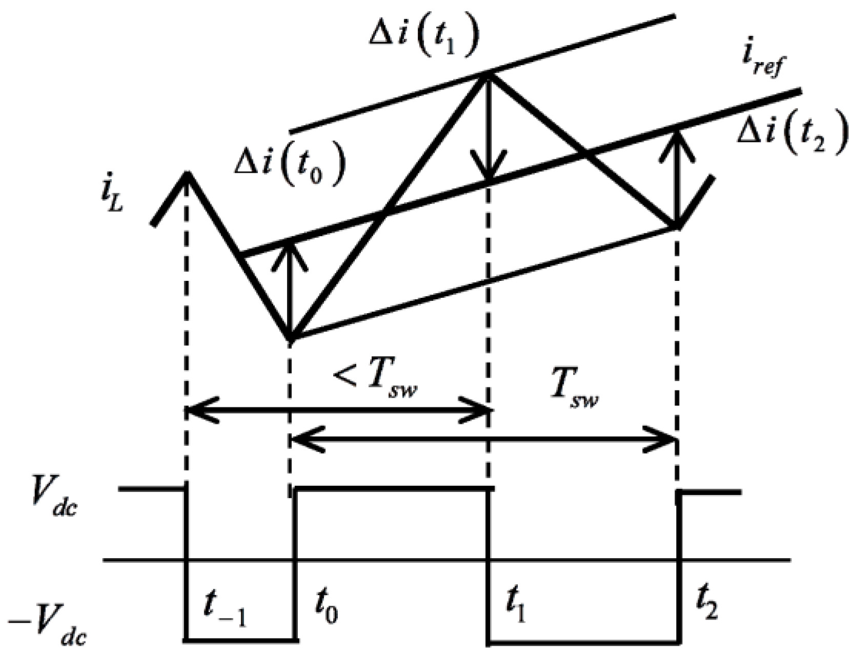
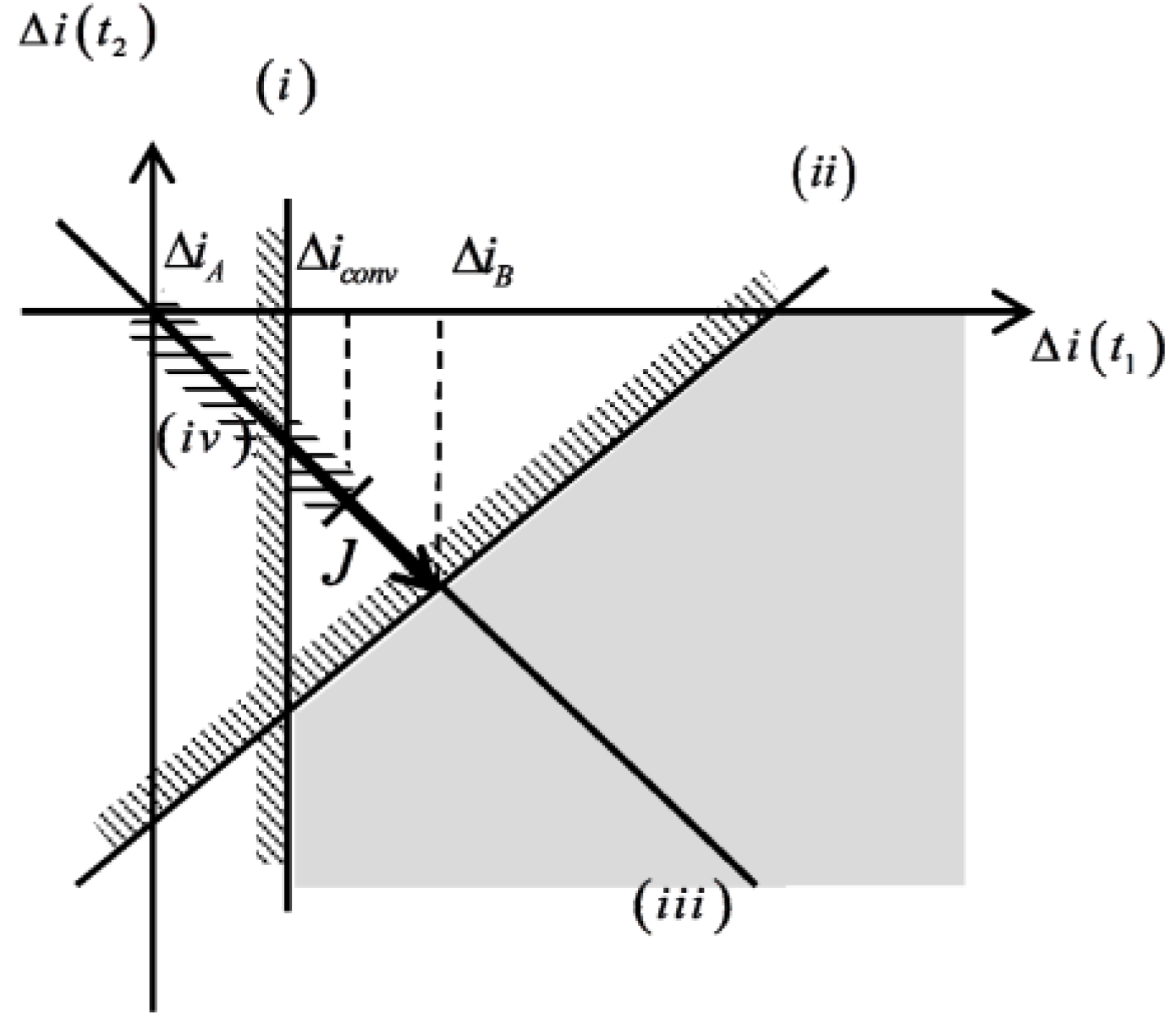
3.2. Disadvantages of Conventional Adaptive Hysteresis Current Control

Consider the case where the inverter needs to be controlled so that the operating switching frequency is always strictly equal to or lower than a constant frequency, which may be the highest possible switching frequency of the switching devices.
The conventional adaptive hysteresis current control described in Section 3.1 has been shown to be able to improve on the disadvantage of the fixed band hysteresis current control of the varying switching frequency [8]. However, when the inverter is operated under the effect of noise or disturbances, this conventional method does not guarantee a stable response and constant switching frequency as, for example, in the following problems.
Problem 1.
If the negative half switching period of switch S 1 in the previous modulation period is T o f f _ p r e , as shown in Figure 5, then:
T o f f _ p r e = t 0 t 1
While the operating switching frequency can be defined from both the time periods T o n + T o f f and T o f f _ p r e + T o n , the calculation of the conventional hysteresis current band only guarantees that modulation period T o n + T o f f is equal to the desired constant switching period T s w , as in Equation (21). If the noise or disturbances to voltage and current make the negative half switching period T o f f _ p r e in the previous modulation shorter than the calculated value, then the operating switching frequency of the conventional method may exceed the highest possible switching frequency of the switching devices.
Problem 2.
In order to keep the average value of the output current equal to the reference current in each switching modulation, the hysteresis current band should be computed so that:
Δ i ( t 1 ) =   Δ i ( t 2 )   = Δ i b
However, the hysteresis current band computed by the conventional method, as in Equations (19) and (20), in general, does not satisfy the Condition (26), except in the case of the ideal condition shown by the dashed line in Figure 6, where the current error at instant t 0 is identical to the computed hysteresis current band Δ i b , i.e.,:
Δ i ( t 0 ) =   Δ i b
When the Condition (27) is not satisfied, the average value of the output current during a switching modulation period deviates from the reference current, which may lead to an unstable response as shown in Figure 6 by the solid line.

4. Proposed Robustly Adaptive Hysteresis Current Control

Consider the instant t 0 , when the output current crosses to pass the lower limit of the hysteresis band i r e f + Δ i ( t 0 ) and the switch S 1 starts to be switched on as shown in Figure 7. The negative half switching period of switch S 1 in the previous modulation period T o f f _ p r e is:
T o f f _ p r e = t 0 t 1 .
In order to solve the problem of unstable switching frequency of the conventional adaptive hysteresis current control mentioned in Section 3, this study proposes a new hysteresis current band computation method by setting an optimization problem as:
( i ) T o f f p r e + T o n T s w , ( i i ) T o n + T o f f T s w , ( i i i ) Δ i b = Δ i ( t 1 )   = Δ i ( t 2 ) , ( i v ) Δ i b Δ i c o n v , minimize Δ i J = ( Δ i ( t 1 ) ) 2   + ( Δ i ( t 2 ) ) 2 ,
where Δ i c o n v is the hysteresis current band computed by the conventional method as in Equation (22), and J is the objective function.
Constraint conditions (i) and (ii) in Equation (29) maintain the operating switching frequency to always be equal to or smaller than the desired instant switching frequency. Condition (iii) keeps the average value of the output current identical to the reference current during the switching modulation period. Condition (iv) keeps the output current from deviating from the reference current. The objective function J represents the power loss from the inverter in each switching modulation period. The hysteresis current band is computed such that the power loss J is minimized.
Equations (15) and (16) can be written as:
T o n = 1 I ˙ o n ( Δ i ( t 1 ) Δ i ( t 0 ) ) ,
T o f f = 1 I ˙ o f f ( Δ i ( t 2 ) Δ i ( t 1 ) )
Substituting Equations (30) and (31) into Equation (29), the optimization problem (29) can be written as:
( i ) Δ i ( t 1 ) I ˙ o n ( T s w T o f f p r e ) + Δ i ( t 0 ) , ( i i ) ( 1 I ˙ o n I ˙ o f f ) Δ i ( t 1 ) + I ˙ o n I ˙ o f f Δ i ( t 2 ) I ˙ o n T s w + Δ i ( t 0 ) , ( i i i ) Δ i ( t 1 )   = Δ i ( t 2 ) = Δ i , ( i v ) Δ i Δ i c o n v , minimize Δ i J = ( Δ i ( t 1 ) ) 2   + ( Δ i ( t 2 ) ) 2 .
The constraints in the optimization problem given in Equation (32) are linear. They can be solved by using the graphical method for minimization problems [27], as below. The feasible region representing constraint conditions (iiv) can be represented by the dark area on the phase-plane ( Δ i ( t 1 ) , Δ i ( t 2 ) ) as in Figure 8. The objective function J is represented by the distance from the original phase-plane to the point ( Δ i ( t 1 ) , Δ i ( t 2 ) ) . Thus, the optimal solution for Problem (32) is the point ( Δ i ( t 1 ) s , Δ i ( t 2 ) s ) on the feasible region, which is closest to the original point. The solution can be derived as:
Δ i o p t = max ( Δ i c o n v , Δ i A , Δ i B ) ,
where Δ i A , Δ i B , Δ i c o n v are the points which satisfy pair constraint conditions (i, iii), (ii, iii), (iv, iii), respectively, and are given by:
Δ i A = I ˙ o n ( T s w T o f f p r e ) + Δ i ( t 0 ) ,
Δ i B = I ˙ o n T s w + Δ i ( t 0 ) 1 2 I ˙ o n / I ˙ o f f ,
Δ i c o n v = 1 2 I ˙ o n I ˙ o f f I ˙ o f f I ˙ o n T s w
When the optimal solution is at Δ i A , it means that, for example under the effect of noise, the negative half switching period T o f f _ p r e in the previous switching modulation was smaller than the regular value (Problem 1 in Section 3) and the hysteresis current band needs to be broadened to satisfy condition (i) in Equation (29). When the optimal solution is at Δ i B , it means that the average output current deviated from the reference current (Problem 2 in Section 3) and the hysteresis current band needs to be broadened to satisfy condition (ii) in Equation (29). When the optimal solution is at Δ i c o n v , it means that the conditions (i) and (ii) are satisfied and the hysteresis current band should be brought to the steady state as in the conventional method.
Remark 1.
In an ideal state, where the effect of noise is sufficiently small, the proposed method gives the same hysteresis current band as the conventional adaptive hysteresis current control method.

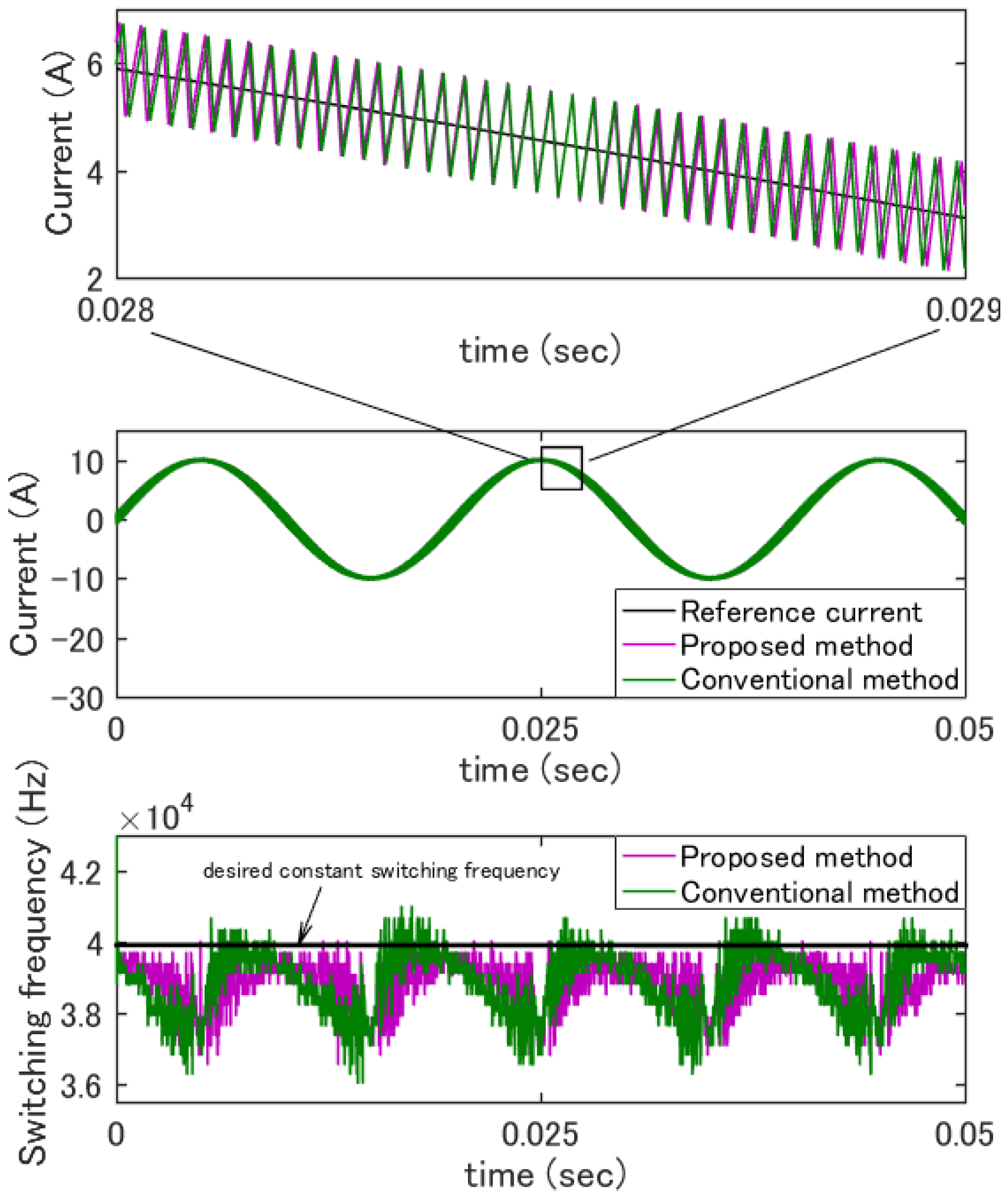
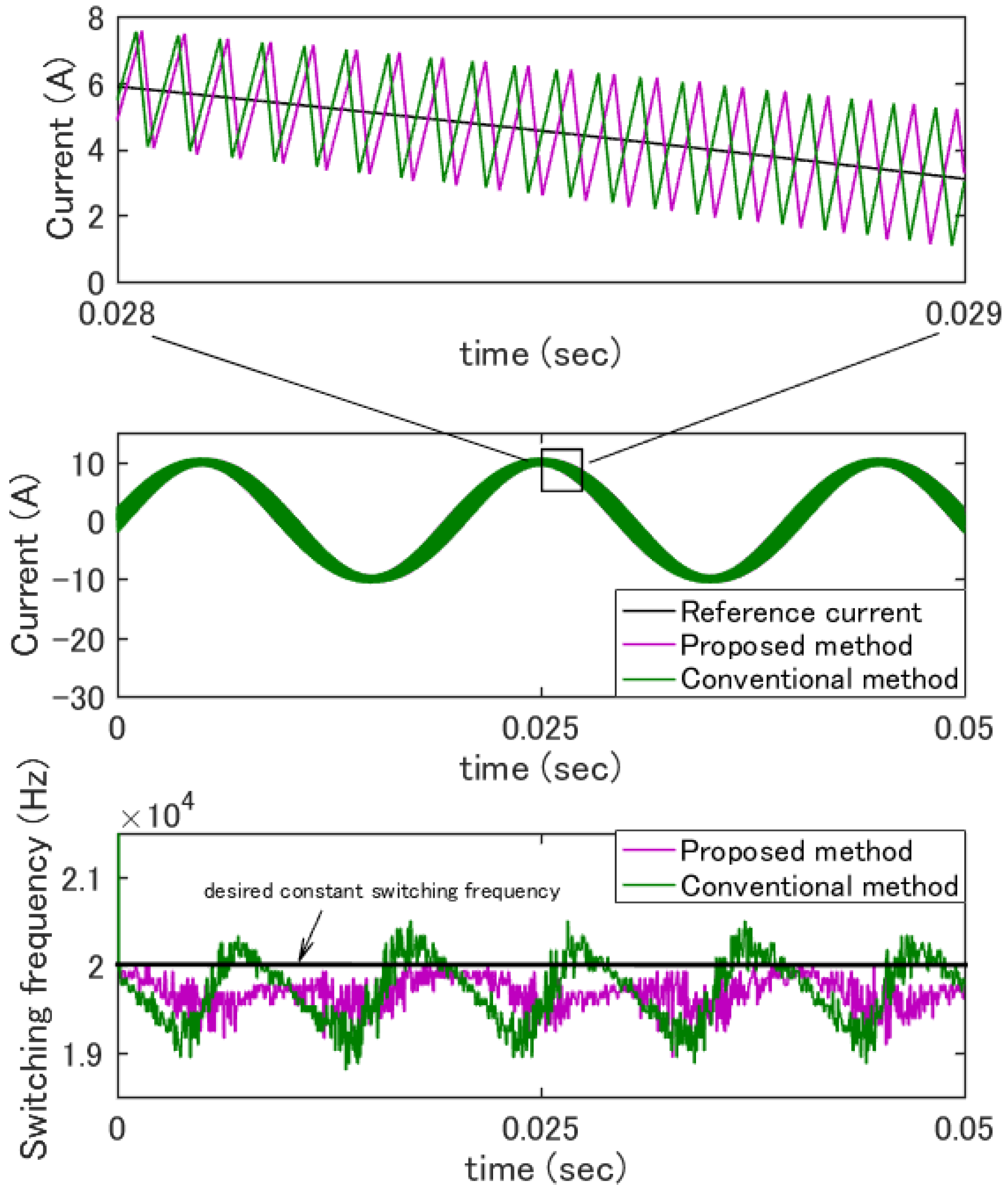
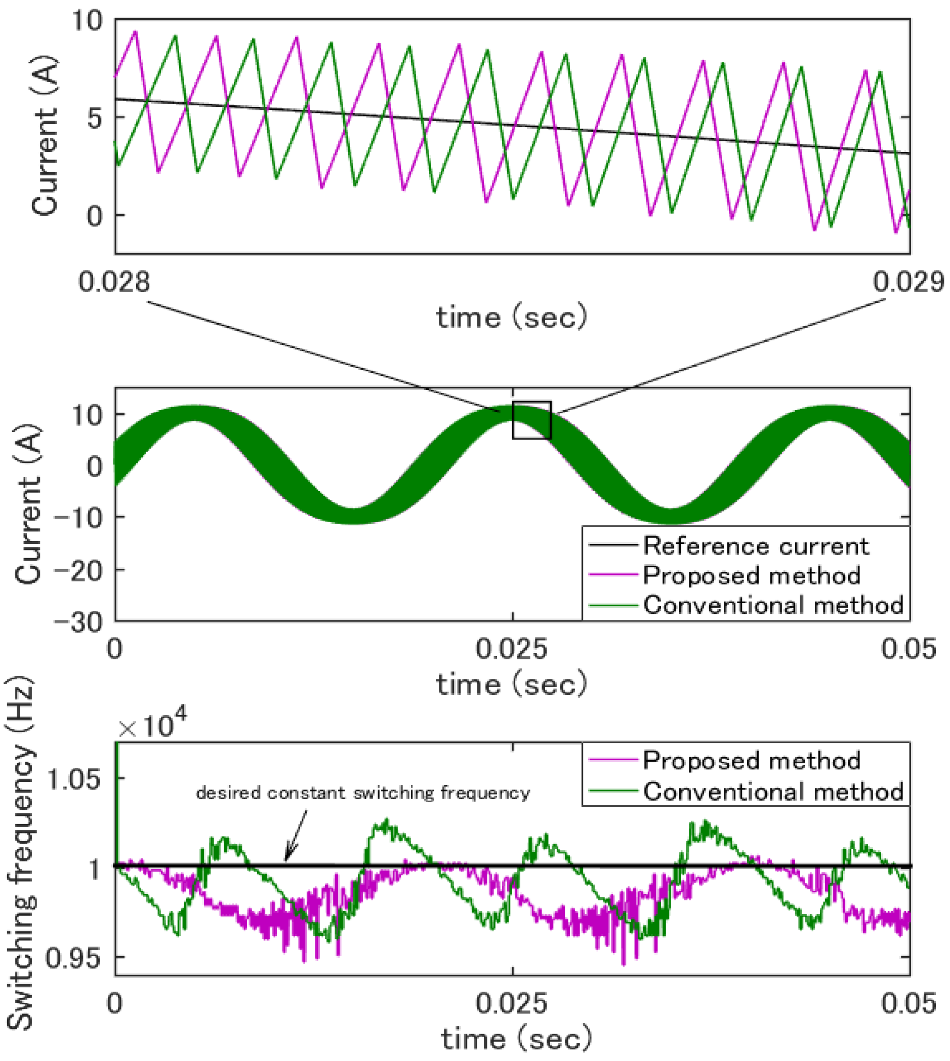
5. Simulation Results

Simulations have been carried out to assess the performance of the proposed method as compared with the conventional method [13] using the Matlab-Simscape Power System. A single-phase half-bridge inverter was employed with the following parameters: an output inductance of L = 1 mH and a filter capacitor of C = 10 μ F. The switching transistors in the inverter circuit were modeled by the Insulated Gate Bipolar Transistor (IGBT) block in the Matlab-Simscape(R2016a, MathWorks, Natick, MA, USA) Power System. The IGBTs have internal and snubber resistances of 1 mΩ and 1 kΩ, respectively. The inverter was connected to the dc voltage source V d c = 175 V, and the ac voltage of the grid was v g = 100 2 sin ( 100 π t ) V. The sampling frequency of the analog/digital converters was f s p = 2 MHz. The reference current was set at i r e f = 10 sin ( 100 π t ) A. The noise in the measured current, which may have come from the current sensor or the analog/digital converter, was assumed to be white noise with a variance of 0.01 A. Figure 9, Figure 10 and Figure 11 show the operating switching frequencies and the output currents of the proposed and conventional methods compared with the reference current for the desired constant switching frequency f s w at 40 kHz, 20 kHz, and 10 kHz respectively. The upper sub-figures show a part of the current hysteresis response. Regarding the desired constant switching frequencies, both methods yielded hysteresis output currents that were similar to the reference current. However, the operating switching frequency of the conventional method oscillated and went over the desired constant switching frequency. On the other hand, the proposed method yielded a switching frequency that was more stable than that of the conventional method and was always maintained at equal to or lower than the desired constant switching frequency. All the Figures also show that the hysteresis current band increased when the desired constant switching frequency was increased.
The power efficiency of the inverter has been calculated, taking into account hysteresis current loss. Table 2 shows the power efficiencies of the proposed and conventional methods with the tested switching frequencies. The efficiencies of both methods decreased when the switching frequency was decreased. It can be seen that the proposed method performed better than the conventional method in terms of power efficiency in all cases.

6. Conclusions

A new digital hysteresis current control algorithm for single-phase half-bridge inverters has been proposed. By taking advantage of digital controls, the hysteresis current band is computed in each switching modulation period based on both the negative half switching period and the current error during the previous switching modulation period, in addition to the usual measured voltage value at the instant of computing. The hysteresis current control, with its simplicity and its fast and stable response, may be implemented on high-speed FPGA boards with a high sampling frequency. The proposed algorithm for computing the hysteresis current band is derived by solving the optimization problem where (i) the switching frequency is stable and always maintained at equal to or lower than the desired constant frequency; (ii) the output current is kept stable around the reference current; and (iii) the power loss is minimized. Although the proposed control method has not been evaluated in experiments, the theoretical numerical and simulation results show good performance of the proposed algorithm compared with those of the conventional method. The proposed method is expected to contribute to the control theory of high-speed FPGA-based hysteresis current control.

Author Contributions

Triet Nguyen-Van, Rikiya Abe, Kenji Tanaka performed and discussed the research; Triet Nguyen-Van carried out the simulations, analyzed the data, and wrote the paper.

Conflicts of Interest

The authors declare no conflict of interest.

References

  1. Justo, J.J.; Mwasilu, F.; Lee, J.; Jung, J.-W. AC-microgrids versus DC-microgrids with distributed energy resources: A review. Renew. Sustain. Energy Rev. 2013, 24, 387–405. [Google Scholar] [CrossRef]
  2. Khayyer, P.; Ozguner, U. Decentralized Control of Large-Scale Storage-Based Renewable Energy Systems. IEEE Trans. Smart Grid 2014, 5, 1300–1307. [Google Scholar] [CrossRef]
  3. Abe, R.; Taoka, H.; McQuilkin, D. Digital Grid: Communicative Electrical Grids of the Future. IEEE Trans. Smart Grid 2011, 2, 399–410. [Google Scholar] [CrossRef]
  4. Liu, C.-C.; McArthur, S.; Lee, S.-J. Smart Grid Handbook; Wiley: West Sussex, UK, 2016. [Google Scholar]
  5. Marian, P.K.; Krishnan, R.; Blaabjerg, F.; Irwin, J.D. Control in Power Electronics Selected Problems; Academic Press: San Diego, CA, USA, 2002. [Google Scholar]
  6. Séguier, G.; Labrique, F. Power Electronic Converters: DC-AC Conversion; Electric Energy Systems and Engineering Series; Springer: Berlin, Germany; New York, NY, USA, 1993. [Google Scholar]
  7. Vazquez, G.; Rodriguez, P.; Ordonez, R.; Kerekes, T.; Teodorescu, R. Adaptive hysteresis band current control for transformerless single-phase PV inverters. In Proceedings of the 35th Annual Conference of IEEE. Industrial Electronics IECON, Porto, Portugal, 3–5 November 2009. [Google Scholar]
  8. Buso, S.; Malesani, L.; Mattavelli, P. Comparison of current control techniques for active filter applications. IEEE Trans. Ind. Electron. 1998, 45, 722–729. [Google Scholar] [CrossRef]
  9. Buso, S.; Fasolo, S.; Malesani, L.; Mattavelli, P. A dead-beat adaptive hysteresis current control. IEEE Trans. Ind. Appl. 2000, 36, 1174–1180. [Google Scholar] [CrossRef]
  10. Kale, M.; Ozdemir, E. An adaptive hysteresis band current controller for shunt active power filter. Electr. Power Syst. Res. 2005, 73, 113–119. [Google Scholar] [CrossRef]
  11. Bose, B.K. An adaptive hysteresis-band current control technique of a voltage-fed PWM inverter for machine drive system. IEEE Trans. Ind. Electron. 1990, 37, 402–408. [Google Scholar] [CrossRef]
  12. Malesani, L.; Mattavelli, P.; Tomasin, P. Improved constant-frequency hysteresis current control of VSI inverters with simple feedforward bandwidth prediction. IEEE Trans. Ind. Appl. 1997, 33, 1194–1202. [Google Scholar] [CrossRef]
  13. Poulsen, S.; Andersen, M.A.E. Hysteresis controller with constant switching frequency. IEEE Trans. Consum. Electron. 2005, 51, 688–693. [Google Scholar] [CrossRef] [Green Version]
  14. Attaianese, C.; Monaco, M.D.; Tomasso, G. High Performance Digital Hysteresis Control for Single Source Cascaded Inverters. IEEE Trans. Ind. Inform. 2013, 9, 620–629. [Google Scholar] [CrossRef]
  15. Hao, Y.; Fang, Z.; Feng, Z.; Zhenxiong, W. A Digital Hysteresis Current Controller for Three-Level Neural-Point-Clamped Inverter With Mixed-Levels and Prediction-Based Sampling. IEEE Trans. Power Electron. 2016, 31, 3945–3957. [Google Scholar]
  16. Jens, O.K.; Markus, H.; Andreas, R.; Rolf, R. FPGA-based Control of Three-Level Inverters, in International Exhibition & Conference for Power Electronics. In Proceedings of the Intelligent Motion and Power Quality, Nuremberg, Germany, 17–19 May 2011; pp. 378–384. [Google Scholar]
  17. Nguyen-Van, T.; Abe, R. An Indirect Hysteresis Voltage Digital Control for Half Bridge Inverters. In Proceedings of the 2016 IEEE Global Conference on Consumer Electronics, Kyoto, Japan, 11–14 October 2016. [Google Scholar]
  18. Javier, C.; Domingo, B.; Francesc, G.; Alberto, P.; Francesc, M.; Eduard, A. FPGA-based design of a step-up photovoltaic array emulator for the test of PV grid-connected inverters. In Proceedings of the 2014 IEEE 23rd International Symposium on Industrial Electronics (ISIE), Istambul, Turkey, 1–4 June 2014; pp. 485–490. [Google Scholar]
  19. Ang, S.S.; Oliva, A. Power-Switching Converters, 2nd ed.; Electrical and Computer Engineering; Taylor & Francis: Boca Raton, FL, USA, 2005. [Google Scholar]
  20. Thiyagarajah, K.; Ranganathan, V.T.; Iyengar, B.S.R. A high switching frequency IGBT PWM rectifier/inverter system for AC motor drives operating from single phase supply. IEEE Trans. Power Electron. 1991, 6, 576–584. [Google Scholar] [CrossRef]
  21. Stefan, H.; Eckart, H.; Oleg, Z.; Klaus-Dieter, L.; Gudrun, F. Reducing Inductor Size in High Frequency Grid Feeding Inverters. In Proceedings of the PCIM Europe 2015 International Exhibition and Conference for Power Electronics, Intelligent Motion, Renewable Energy and Energy Management, Nuremberg, Germany, 19–20 May 2015; pp. 196–203. [Google Scholar]
  22. Tooley, M.H. Plant and Process Engineering 360, 1st ed.; Butterworth-Heinemann: Amsterdam, The Netherlands; Boston, MA, USA; London, UK, 2010. [Google Scholar]
  23. Pei, X.; Kang, Y. Short-Circuit Fault Protection Strategy for High-Power Three-Phase Three-Wire Inverter. IEEE Trans. Ind. Inform. 2012, 8, 545–553. [Google Scholar] [CrossRef]
  24. Nguyen-Van, T.; Abe, R. New hysteresis current band digital control for half bridge inverters. In Proceedings of the 2016 IEEE International Conference on Consumer Electronics-Taiwan (ICCE-TW), Nantou, Taiwan, 27–29 May 2016. [Google Scholar]
  25. Zare, F.; Ledwich, G. A hysteresis current control for single-phase multilevel voltage source inverters: PLD implementation. IEEE Trans. Power Electron. 2002, 17, 731–738. [Google Scholar] [CrossRef] [Green Version]
  26. Buso, S.; Caldognetto, T. A non-linear wide bandwidth digital current controller for DC-DC and DC-AC converters. IEEE Trans. Ind. Electron. 2015, 62, 7687–7695. [Google Scholar] [CrossRef]
  27. Baker, K.R. Optimization Modeling with Spreadsheets, 3rd ed.; Wiley: West Sussex, UK, 2015. [Google Scholar]
Figure 1. Single-phase half-bridge inverter circuit.
Energies 10 01610 g001
Figure 2. Structure of the digital control system.
Energies 10 01610 g002
Figure 3. Fixed band hysteresis current control.
Energies 10 01610 g003
Figure 4. Conventional adaptive hysteresis current control.
Energies 10 01610 g004
Figure 5. Conventional adaptive hysteresis current control does not guarantee that the operating switching frequency will be lower than the desired constant frequency.
Energies 10 01610 g005
Figure 6. Conventional adaptive hysteresis current control does not guarantee the stability of the response current.
Energies 10 01610 g006
Figure 7. Proposed adaptive hysteresis current control.
Energies 10 01610 g007
Figure 8. Domain and optimal solution for the hysteresis current band.
Energies 10 01610 g008
Figure 9. Current and switching period of the proposed method and conventional method for the desired switching frequency at 40 kHz.
Energies 10 01610 g009
Figure 10. Current and switching period of the proposed method and conventional method for the desired switching frequency at 20 kHz.
Energies 10 01610 g010
Figure 11. Current and switching period of the proposed method and conventional method for the desired switching frequency at 10 kHz.
Energies 10 01610 g011
Table 1. States of switches and corresponding outputs.
Half PeriodS1S2Input Voltage vdcOutput Current iL
PositiveOnOff V d c Increase
NegativeOffOn V d c Decrease
Table 2. Power efficiency with various switching frequencies (%).
Switching frequency f s w = 10 kHz f s w = 20 kHz f s w = 40 kHz
Proposed method97.198.499.3
Conventional method95.297.298.5

