Abstract
In the application of rail transit vehicles, when using typical wireless power transfer (WPT) systems with series–series (SS) compensation supply power for supercapacitors, the output current is in an approximately inverse relationship with the duty cycle in a wide range. This renders the typical buck circuit control inappropriate. In order to help resolve the above issues, this paper designs inductor/capacitor/capacitor (LCC) compensation with new compensation parameters, which can achieve an adjustable quasi-constant voltage from the input of the inverter to the output of the rectifier. In addition, the two-port network method is used to analyze the resonant compensation circuit. The analysis shows that LCC compensation is more suitable for the WPT system using the supercapacitor as the energy storage device. In the case of LCC compensation topology combined with the charging characteristics of the supercapacitor, an efficient charging strategy is designed, namely first constant current charging, followed by constant power charging. Based on the analysis of LCC compensation, the system has an optimal load, by which the system works at the maximum efficiency point. Combined with the characteristics of the constant voltage output, the system can maintain high efficiency in the constant power stage by making constant output power the same as the optimal power point. Finally, the above design is verified through experiments.
1. Introduction
Wireless power transfer (WPT) systems have been widely developed for applications to rail transit vehicles because they avoid direct electrical connection, which can help eliminate the danger of electrical sparks and provide automatic power supply [1,2,3,4]. In recent years, some initiatives (Bombardier´s PRIMOVE and South Korea´s KAIST) have introduced the WPT technology power supply mode combined with the energy storage-type tram [5,6] to provide more convenient and safe traffic vehicles. Such vehicles do not require a large number of energy storage devices, and this can help make the vehicle more lightweight. In addition, the WPT system renders the power supply safer and more reliable, thus reducing the influence of environmental conditions.
For this type of WPT system applied in rail transit vehicles, a three-phase rectifier is used to convert the grid alternating current (AC) to the direct current (DC) bus voltage. The primary-side coil is typically fed with a high-frequency AC current, which is converted via a single-phase inverter, and generates an AC magnetic flux linkage. Then, a secondary-side coil will induce an AC current to supply power to the load. The electrical equipment requires a small DC voltage and/or a current ripple, an AC/DC rectifier, and a DC/DC converter consisting of a regulation circuit, which is typically connected between it and the load. The topology is displayed in Figure 1.
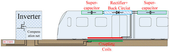
Figure 1.
Wireless power transfer (WPT) system configuration in rail transit vehicles.
In the WPT system, resonance compensation design is an important method by which suitable characteristics of the system may be achieved, such as constant voltage or constant current. Authors in [7] propose a series-parallel/series (SPS) compensation topology which can ensure that the load stabilizes the active power even if there is alignment error in the coupling coils, while the input resistance of the inverter is much higher. In [8], the characteristics of SS compensation and PS compensation are analyzed, and a method is proposed to improve the efficiency in the full range by switching compensation. Other resonant compensations, such as inductor/capacitor/inductor (LCL), and inductor/capacitor/capacitor/inductor (LCCL), are found in [9,10,11]. These papers focus on improving performance indicators such as system efficiency, transfer power level and so on, and give the corresponding resonant compensation design criteria. Authors of [12,13] describe how to achieve resonant compensation design to obtain a soft switching inverter. For the battery load, the system efficiency, transfer power and voltage gain are analyzed under the condition of SS compensation [14,15].
The above research focuses on the resistance or battery load, but the energy storage device is typically a supercapacitor, so as to meet the demand of fast charging. There has been no further research on resonant compensation considering the WPT system with a supercapacitor as the load.
Considering the supercapacitor to be the load of the WPT system, and adding buck circuit to control the charging current, it is hoped that the DC voltage after the secondary-side rectifier is constant so as to easily control the output power. The typical series–series (SS) compensation method [16,17] is unable to meet such requirements. The compensation structures which have constant voltage output are the series/parallel (SP) compensation [18], LCL compensation [9] and the secondary-side controlled rectifier [14]. However, the SP compensation voltage gain is too high, while the LCL compensation voltage gain is too low for high power level WPT systems, and the controllable rectifier renders the control too complex. In order to resolve these issues, this paper presents a compensation structure which includes primary-side LCC compensation and the secondary-side series compensation (known as LCC compensation), and gives the design of the compensation parameters. This LCC compensation can achieve adjustable quasi-constant voltage output to make input voltage of the secondary buck circuit work at the constant value. The primary side and secondary side of WPT system can be separated structures, and this can therefore reduce the information interaction between the primary side and secondary side. In addition, combined with the charging requirements of the supercapacitor, an efficient charging strategy is proposed to allow the WPT system to work in optimal efficiency conditions.
The organization of this paper is as follows: The model and analysis or the WPT system is shown in Section 2. The problems of SS compensation are given and the LCC compensation analysis is carried out. Next, Section 3 proposes the supercapacitor charging strategy using the WPT system, and system efficiency is given. In Section 4, an experimental prototype is fabricated to achieve the WPT system power supply for the supercapacitor (SC), and to verify the theory correctness of the LCC compensation topology and feasibility of the supercapacitor charging strategy. Finally, conclusions are given.
2. Model and Analysis of the WPT System
2.1. Mode of SS Compensation Cascade Buck Circuit
In the application of rail transit, the bidirectional DC/DC converter is used to realize the function of charging/discharging an SC. The bidirectional DC/DC is equivalent to the buck converter when charging for an SC. When using a WPT system that adopts the typical SS compensation mode supplying power to an SC, the buck converter will cascade after the rectifier, and the system can be defined as the SS compensation cascade buck circuit mode as shown in Figure 2.
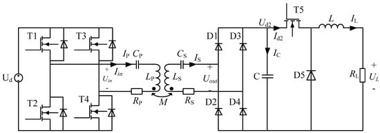
Figure 2.
Series–series (SS) compensation cascade buck circuit mode.
The system consists of DC bus voltage, an inverter (working at tens of kHz), the primary- and secondary-side coils, a rectifier, a buck converter and a load, where Ud is the DC bus voltage, UL/IL is the load voltage/current, Uin/Iin is the input voltage and current of the coupling coils, Uout is the output voltage of the coupling coils, IP and IS are the root-mean-square (RMS) values of the primary- and secondary-side currents, respectively, and Ud2 is the DC voltage after rectifier. T1–T4 are the full-bridge semiconductor switches, D1–D4 are the rectifier diodes, RP (RS), LP (LS) and CP (CS) are the primary (secondary) side coil resistance, inductance and series compensation capacitors respectively, M is the mutual inductance of the primary- and secondary-side coils, and C and L are the DC side filter inductor and capacitor, respectively. Finally, T5/D5 is the semiconductor switch and diode of the buck converter, and RL is the load resistance.
In order to simplify the analysis of the transfer characteristics of the system, the SS compensation WPT system may be arranged as shown in Figure 3. According to Kirchhoff’s voltage law, the following equations are obtained:
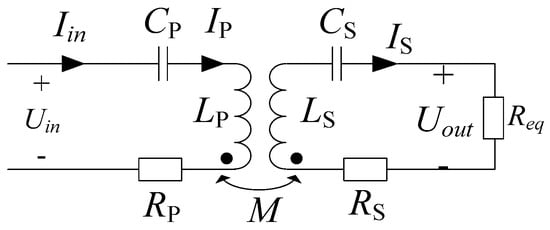
Figure 3.
SS compensation equivalent circuit.
The operating frequency ω is the angular frequency of the high frequency inverter, IP and IS are the primary and secondary side current. Based on the working principle of the rectifier and buck circuit, the relationship between the output equivalent resistance of coupling coils (Req) and load resistance (RL) is achieved as follows,
where D is the duty cycle of the buck circuit.
In order to reduce the power converter volt-ampere (VA) rating and improve the transfer efficiency of the system [19], the compensation capacitance parameters are determined by Formula (3) in the SS compensation topology.
The secondary side current IS can be calculated according to Formulas (1) and (3):
According to the relationship of the parameters of input/output voltage and current of the rectifier and buck circuit, the load current can be determined as follows:
When Uin and M are fixed values, the relationship between D and IL is as shown in Figure 4. The parameters of SS compensation are shown in Table 1. It can be found that when the D is gradually increased, the IL first increases and then decreases, and the maximum value of IL is obtained when the critical value of Db is equal to that shown in Formula (6). RP is a relatively low value, thus the critical value of Db is very small. In a large range of Db < D < 1, the load current IL and duty cycle D present an approximate inverse proportion of the variation. The mode of the SS compensation cascade buck circuit is different from the typical buck converter, in which the relationship between IL and D is a monotone function. Therefore, the WPT system needs to be designed suitably, and then the Buck converter can be used with a dynamic changing input voltage and the constant output voltage/current is adjusted using the proportional integral (PI) control strategy [20]. However, for practical applications, the buck circuit is expected to have constant input voltage for reliable control.
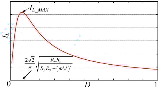
Figure 4.
The relationship between D and IL.

Table 1.
Experiment platform parameters.
Using Formula (7), it can be found that the reason for this is that the variations of duty cycle D will result in the change of the output voltage of the rectifier Ud2, and is thus inversely proportional to D2.
In order to allow the input voltage of the secondary buck circuit to work at the constant value, the secondary-side voltage needs to be constant or nearly constant. The primary side and secondary side of WPT system are expected to be separated structures, therefore interaction of information between the primary side and secondary side can be reduced.
Considering the above factors, this paper redesigns the LCC resonance compensation topology to achieve the constant output voltage characteristics of the buck circuit.
2.2. LCC Compensation Topology Analysis
In view of the above problems, this paper proposes a compensation topology. The mode by which the primary side provides LCC compensation and secondary side provides series compensation has the characteristic of quasi constant voltage output, which can allow the buck circuit to use the traditional control method. In addition, this mode has adjustable voltage gain and is suitable for the application of a high power WPT system.
Figure 5 shows the principle of the resonant compensation topology. Resonant inductance Lr and capacitor Cr are additional elements compared with SS resonant compensation mode, RLr is the self-resistance of Lr.
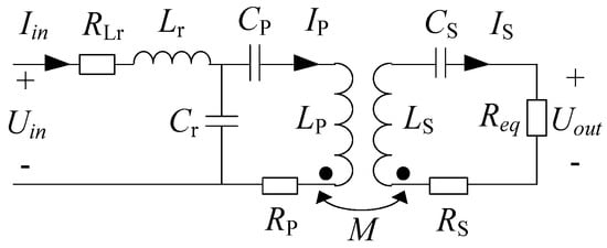
Figure 5.
LCC compensation equivalent circuit.
According to the principle of the circuit, the secondary-side coil parameters are converted to the primary-side system, as shown in Figure 6a, ZRE is the reaction impedance. The secondary side is series resonant compensation method, so the reaction impedance ZRE can be calculated as follows,
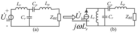
Figure 6.
Equivalent transformation of LCC compensation.
To achieve constant output voltage of the receiving side, it is necessary to meet the requirement that the primary-side coil current is constant. Then, in the case of secondary-side series compensation, the constant voltage output can be achieved. According to the Norton theorem, LLC compensation circuit can be equivalent to that shown in Figure 6b. Therefore, in the case of constant-voltage-source input, the constant-current-source can be obtained by series inductor Lr. If the parallel compensation capacitor Cr is resonant with Lr, the constant current characteristic of the primary-side coil can be achieved. As shown in Figure 6b. The constant current value of the primary-side coils can be obtained when the self-resistance of inductance is ignored:
The values of LS, CS, Cr and Lr are given by the following formula
To reduce the power converter VA rating, the primary-side capacitor is typically tuned so that the input voltage and current is in zero-phase under certain coupling and load conditions, and the value of the capacitor CP is determined by the following formula:
According to (10) and (11), CP can be determined:
Next, the two-port network theory [19] is introduced to analyze the equivalent circuit of the primary side, and the system has constant-voltage-source input as shown in Figure 7, where URE and IRE are the voltage and current of the reactance resistance.
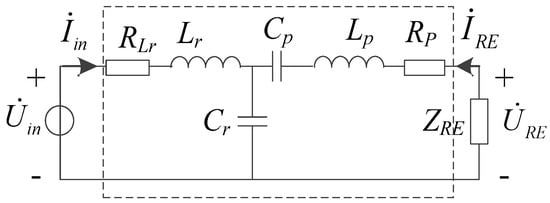
Figure 7.
Two port network of LCC compensation.
As the input type of LCC compensation system is a voltage source, a two-port network [21] can be expressed as follows:
where
When the parameters satisfy the compensation requirements of (10) and (12), Equations (14)–(17) can be simplified as follows:
Therefore, the output and input voltage gain of the two-port network is:
The voltage gain of the output of the coupling coil to the reactance resistance can be calculated as:
It can be concluded that the voltage gain from the output of the inverter to the output of the coupling coil is as follows:
Under the condition of ignoring the self-resistance of the coils and the resonant inductance, the voltage gain (HU) can be simplified as:
HU can be approximated as the ratio of M and Lr, and when the equivalent resistance Req changes, Uout can be maintained as a quasi-constant state. In addition, when the duty cycle of the buck circuit is changed, the secondary-side DC bus voltage Ud2 will remain in the quasi-constant state. Furthermore, if M is determined, then the voltage gain of the system can be adjusted by the appropriate choice of the Lr value.
According to the parameters shown in Table 1, Figure 8 shows the comparison of the voltage gain between the SS compensation and LCC compensation. It can be found that the LCC topology has a more stable voltage gain even if the load changes.
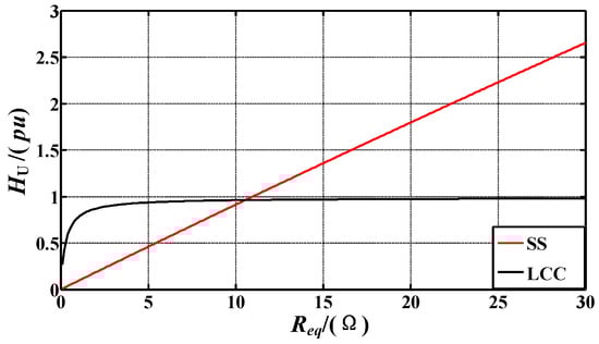
Figure 8.
The comparison of the voltage gain between SS and LCC compensation.
The output current of the inverter Iin and primary-side coil current IP can be calculated according to the characteristics of the two port network,
Ignoring the self-resistance of the coils and the resonant inductance, (23) and (24) can be simplified as follows:
When the parking error causes the decrease of the mutual inductance, the output current of the inverter will reduce according to Equation (25), which ensures the safe operation of the system. When the inverter output voltage Uin is fixed, the current flow through the primary-side coil IP has a quasi-constant current characteristic according to Equation (26) which is consistent with Equation (9). The quasi-steady characteristic of IP leads to the primary coil magnetic field stability which guarantees the transmission of electrical energy. This also proves that the LCC compensation topology has better fault tolerance ability and is more suitable for application in rail transit.
3. Supercapacitor Charging Strategy Using WPT System
3.1. Characteristics Analysis of Super Capacitor Load
The supercapacitor is typically used as the energy storage device in rail transit vehicles due to its advantage of high power density, and the equivalent circuit of the supercapacitor can be seen in Figure 9. When the WPT system charges for the supercapacitor, the voltage and current of supercapacitor will change in real time due to the charging process. This paper adopts an equivalent variable resistance RL to represent the supercapacitor. The relationship between them can be determined as follows:
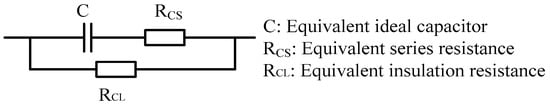
Figure 9.
Simplified equivalent model of the supercapacitor.
The instantaneous equivalent load value RL is the ratio of the supercapacitor voltage and the charging current.
The use of supercapacitor is typically based on the charge and discharge curve. The most common method is constant current charging at the beginning, followed by adopting low charging current charging to the rated voltage when the supercapacitor reaches rated voltage. This paper considers the constant power charge to the rated voltage. The charging curve is shown in Figure 10.
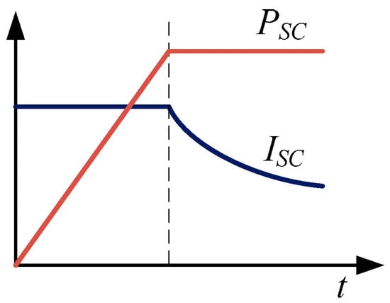
Figure 10.
Supercapacitor (SC) charging method.
The charging process will have an effect on the characteristics of the WPT system. Considering the supercapacitor´s charging features, this paper proposes a new segmented charging strategy for the supercapacitor using the LCC compensation-mode WPT system. The following subsection will provide an introduction.
3.2. Segmented Charging Strategy
The supercapacitor charging process is divided into two stages, namely the constant current and constant power stage. In the constant current stage, the LCC compensation mode can ensure that the output voltage of the rectifier remains constant, which signifies that the input voltage of the buck converter is constant. Therefore, the constant charging current of the supercapacitor is easily achieved by controlling the buck circuit, and the control method can use PI control to adjust the duty cycle of the buck circuit. This is consistent with the typical control of the buck circuit.
When the supercapacitor voltage increases to the reference voltage value USC* at the end of the constant current charging, it will enter the constant power charging stage. The system efficiency is more important when USC is in the range from the reference voltage USC* to the rated voltage UMAX, as the charging power is greater. This provides a constant power charging strategy based on the LCC compensation method to maintain a high charging efficiency of the WPT system.
The current gain of the two port network is determined as follows:
When the system is under the resonance and when the converter (including inverter, rectifier and buck converter) losses are ignored the system efficiency expression can be obtained:
According to the formula of GU and GI, the system efficiency based on LLC compensation can be expressed as follows:
Considering the system parameters listed in Table 1, the relationship between η and Req is shown in Figure 11 according to (30). In the process of the equivalent load Req gradually increases. The system efficiency will first increase, then decrease, which is similar with the SS compensation mode. If the output equivalent resistance of the coupling coil is the optimal load Ropt, the system can maintain the efficient operation, namely Req = Ropt, and then the system achieves maximum efficiency.
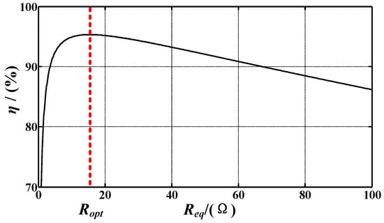
Figure 11.
The relationship between η and Req.
By differentiating η with respect to Req and equating the differential function to zero,
The optimum value Ropt for maximum efficiency can be obtained as follows:
As the self-resistance (RP, RS, RLr) is further decreased, the reactance (ωM, ωLr), Ropt can be simplified as shown in (33),
When the load RL changes, it is found that the duty cycle of the buck circuit can be adjusted to make Req = Ropt according to Formula (2) which can ensure that the system has been working at the maximum efficiency point. In order to simplify the control difficulty in the actual control, combined with Formula (22) the optimal load control can be converted to optimal power control. When the output power of system is the constant Popt, the maximum efficiency of the system based on the LCC compensation structure can be obtained:
Based on the above analysis, an efficient charging strategy for the supercapacitor is designed combined with the WPT system, as shown in Figure 12. The supercapacitor voltage and current are detected in real time, and if the supercapacitor voltage USC is smaller than the reference voltage USC*, the buck circuit is controlled under the constant current charging model. When the super capacitor voltage USC is greater than the USC* instruction, then the product of the super capacitor voltage and current is calculated as the supercapacitor charging power, and the constant power reference PSC* is used to adjust the buck circuit duty cycle D to achieve constant power charging.
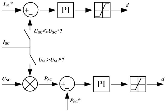
Figure 12.
Charging strategy for supercapacitor.
In order to satisfy the output requirements of the system and maintain high system efficiency, the traditional methods are based on dual-side control, namely the inverter and DC/DC which adjust the efficiency and the output power respectively. This method skillfully uses the characteristics of LCC constant voltage output, further combined with the requirements of the supercapacitor´s constant power supply to design an efficient charging strategy. To a certain extent, system efficiency is improved, and the complicated dual side control is avoided, which can prove the stable operation of the WPT system.
4. Experiment Verification
4.1. Setup of Experiment
In order to verify the constant voltage characteristics of LCC compensation mode and feasibility of the proposed charging strategy, a WPT system experimental prototype is fabricated, and shown in Figure 13. The topology of the WPT system using SC as a load is similar to that shown in Figure 2, but the SS compensation is replaced by LCC compensation. The parameters are consistent with those in Table 2.
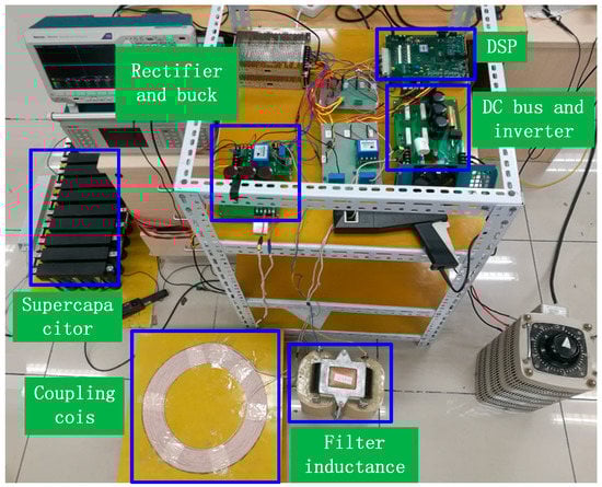
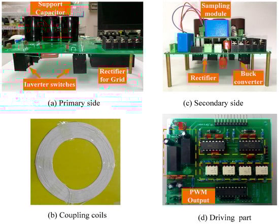
Figure 13.
Demo SC-load wireless power transfer (WPT) system (up) and each part (down).
Table 2.
Experiment platform parameters.
The SanRex three-phase bridge DF100AA160 (Osaka, Japan) is used to convert the grid alternating current (AC) to direct current (DC). CREE SiC MOSFET C2M0080120D (Durham, NC, USA) is adopted as the active switch of inverter (DC/AC) on the 58 kHz switching frequency. CREE SiC SBD C4D20120D (Durham, NC, USA) is used as the anti-parallel diode of the inverter (DC/AC) and the switch of the rectifier (AC/DC). The transmitter and receiver inductors are circular coils with a single layer and a turn number of 18, composed of tightly-wound litz wires with a diameter of 3 mm. The external diameter of coil is 40 cm and the gap between the transmitter and receiver is 15 cm. The inductor and capacitor are chosen under the resonance for both the transmitter and receiver, and the resonant frequency is same as the operating frequency for improving the efficiency and reducing the VA rating of the WPT system. The SC voltage, charging current, transmitter and receiver AC currents and voltages are tested using a Tektronic DPO3034 Digital Phosphor Oscilloscope (Beaverton, OR, USA). Based on the test results, the transmitting power, receiving power and transfer efficiency are calculated using MATLAB software according to the definition of power.
The supercapacitor charging process is as follows. First, constant current (ISC*) charging is performed until the supercapacitor voltage increases to the reference voltage (USC*), the ISC* is 12 A and the USC* is 50 V. Then, when the supercapacitor voltage is greater than USC*, the charging process changes to constant power charging, and the power reference PSC* is 600 W. The capacitance of the supercapacitor is 18 F.
4.2. Setup of Experiment
When supercapacitor charging adopts an efficient charging strategy, the inverter output voltage and current waveform are as shown in Figure 14 under the mode of the constant power. It can be seen that the phase of inverter output voltage is ahead of the current phase. This is because the above theoretical analysis is based on the fundamental waveform, however the output of the inverter is a square wave at three times and has higher harmonics, thus there is only a light phase difference of the voltage and current. This also enables the system to achieve zero voltage switching (ZVS).
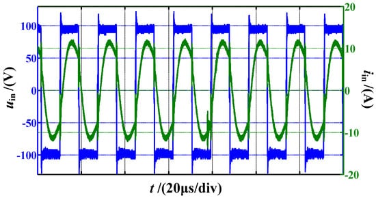
Figure 14.
Output voltage(uin) and current(iin) of the inverter in constant power mode.
Figure 15 shows the waveform of the secondary-side DC bus voltage Ud2 during the supercapacitor charging process. It was found that the amplitude of Ud2 decreased from 100 V to 83 V, which is because with the increase of the output power, the DC bus voltage decreases, and during the constant power process Ud2 is constant. Thus, the voltage gain HU can maintain a quasi-steady state. Since the voltage gain is approximately 1 (corresponding to the ratio value of M and Lr) this verifies the accuracy of the analysis.
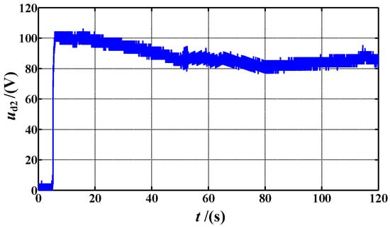
Figure 15.
DC Voltage of rectifier at secondary side.
Figure 16 represents the waveforms of the supercapacitor charging current, charging voltage and charging power. The constant charging power is 593 W, which is essentially in agreement with reference power PSC*. According to the output voltage and current of the inverter as shown in the Figure 14, the inverter output active power (Pin) is obtained as shown in Figure 17. The constant power Pin is 675 W.
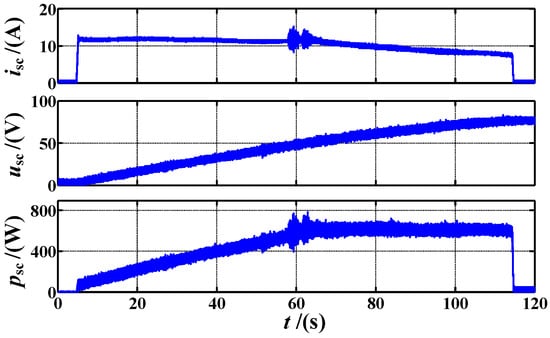
Figure 16.
Voltage, current and power of supercapacitor.
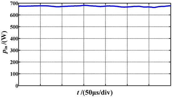
Figure 17.
Output power of the inverter at constant power mode.
The variation of the coupling system efficiency of the charging process is shown in Figure 18. It can be found that during constant current charging, the efficiency will increase and the maximum efficiency will be obtained with constant power charging. That is because the optimal power is obtained. The experimental results are almost the same with the calculation results in accordance with Equation (30), and the maximum efficiency is about 95%.
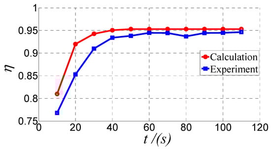
Figure 18.
Calculation and experimental results of the coupling coils efficiency.
According to the experimental results, the overall efficiency of the inverter to the supercapacitor (including the efficiency of the rectifier and the buck circuit) was found to be 87.8% in the constant power stage as shown in Figure 19. Overall efficiency can be maintained at the maximum efficiency point.
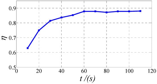
Figure 19.
Experimental results of the overall system efficiency.
The experimental results verify the correctness of the theoretical derivation of the LCC compensation WPT system, and the efficient segmented charging strategy is performed using the experiments.
5. Conclusions
This paper presents a new compensation mode which includes primary-side LCC compensation and secondary-side series compensation, and is based on the deficiency of the typical mode of SS compensation cascade buck circuit. In this manner, the WPT system can achieve adjustable quasi-constant voltage output, which renders the buck circuit control method easier to use and more reliable. This allows the design method of the compensation parameters to achieve adjustable voltage gain. Based on this LCC compensation topology, an efficient supercapacitor segmented charging strategy is proposed, namely first constant current charging and then constant power charging, and the system can be operated efficiently at a constant power stage. Finally, the theory correctness of the LCC compensation topology and feasibility of the supercapacitor charging strategy are verified through experiments.
In future works, the constant power charging process will be optimized further to improve overall system efficiency. For example, the losses of the converter will be considered, such as the loss model of rectifier and buck converter. The charging time of the constant current charging process will be designed under the condition that the charging requirements have been satisfied, such as the charging time and energy.
Acknowledgments
Thanks for Fuji Electric Co., Ltd. support the IGBT devices and Nippon Chemi-con Corporation for supplying the supercapacitor for the experiments.
Author Contributions
Fei Lin contributed to the conception of the study, Yuyu Geng and Bin Li contributed significantly to analysis and manuscript preparation, Zhongping Yang helped perform the analysis with constructive discussions and Hu Sun provided experimental assistance.
Conflicts of Interest
The authors declare no conflict of interest.
References
- Covic, G.A.; Boys, J.T. Modern trends in inductive power transfer for transportation applications. IEEE J. Emerg. Sel. Top. Power Electron. 2013, 1, 28–41. [Google Scholar] [CrossRef]
- Covic, G.A.; Boys, J.T. Inductive power transfer. Proc. IEEE 2013, 101, 1276–1289. [Google Scholar] [CrossRef]
- Shin, J.; Shin, S.; Kim, Y.; Ahn, S.; Lee, S.; Jung, G.; Jeon, S.J.; Cho, D.H. Design and implementation of shaped magnetic-resonance-based wireless power transfer system for roadway-powered moving electric vehicles. IEEE Trans. Ind. Electron. 2014, 61, 1179–1192. [Google Scholar] [CrossRef]
- Yusop, Y.; Saat, S.; Nguang, S.K.; Husin, H.; Ghani, Z. Design of Capacitive Power Transfer Using a Class-E Resonant Inverter. J. Power Electron. 2016, 16, 1678–1688. [Google Scholar] [CrossRef]
- Ko, Y.D.; Jang, Y.J. The Optimal System Design of the Online Electric Vehicle Utilizing Wireless Power Transmission Technology. IEEE Trans. Intell. Transp. Syst. 2013, 14, 1255–1265. [Google Scholar] [CrossRef]
- Cheng, S.; Chen, X.; Wang, J.; Wen, J.; Li, J. Key Technologies and Applications of Wireless Power Transmission. Trans. China Electrotech. Soc. 2015, 30, 68–84. [Google Scholar] [CrossRef]
- Villa, J.L.; Sallan, J.; Sanz Osorio, J.F.; Llombart, A. High-Misalignment Tolerant Compensation Topology for ICPT Systems. IEEE Trans. Ind. Electron. 2012, 59, 945–951. [Google Scholar] [CrossRef]
- Matsumoto, H.; Neba, Y.; Asahara, H. Switched Compensator for Contactless Power Transfer Systems. IEEE Trans. Power Electron. 2015, 30, 6120–6129. [Google Scholar] [CrossRef]
- Zhou, H.; Yao, G.; Zhao, Z.; Zhou, L.; Jiang, D.; Guo, F. LCL Resonant Inductively Coupled Power Transfer System. Proc. CSEE 2013, 33, 9–16. [Google Scholar]
- Yang, M.; Wang, Y.; Ouyang, H. Modeling and Optimizing of a New Contactless ICPT System with Constant Primary Winding Current. Proc. CSEE 2009, 29, 34–40. [Google Scholar]
- Zhang, W.; Mi, C. Compensation Topologies of High Power Wireless Power Transfer Systems. IEEE Trans. Veh. Technol. 2016, 65, 4768–4778. [Google Scholar] [CrossRef]
- Lu, R.; Wang, T.; Mao, Y.; Zhu, C. Analysis and design of a wireless closed-loop ICPT system working at ZVS mode. In Proceedings of the 2010 IEEE Vehicle Power and Propulsion Conference (VPPC), Lille, France, 1–3 September 2010; pp. 1–5.
- Tang, C.S.; Sun, Y.; Su, Y.G.; Nguang, S.K.; Hu, A.P. Determining Multiple Steady-State ZCS Operating Points of a Switch-Mode Contactless Power Transfer System. IEEE Trans. Power Electron. 2009, 24, 416–425. [Google Scholar] [CrossRef]
- Nguyen, B.X.; Vilathgamuwa, D.M.; Foo, G.H.B.; Wang, P.; Ong, A.; Madawala, U.K.; Nguyen, T.D. An Efficiency Optimization Scheme for Bidirectional Inductive Power Transfer Systems. IEEE Trans. Power Electron. 2015, 30, 6310–6319. [Google Scholar] [CrossRef]
- Zhang, Y.; Chen, K.; He, F.; Zhao, Z.; Lu, T.; Yuan, L. Closed-Form Oriented Modeling and Analysis of Wireless Power Transfer System with Constant-Voltage Source and Load. IEEE Trans. Power Electron. 2015, 31, 1. [Google Scholar] [CrossRef]
- Tan, L.; Yan, C.; Huang, X.; Wang, W.; Chen, C. Stable Voltage Online Control Strategy of Wireless Power Transmission System. Trans. China Electrotech. Soc. 2015, 30, 12–17. [Google Scholar]
- Mai, R.; Lu, L.; Li, Y.; He, Z. Dynamic Resonant Compensation Approach Based on Minimum Voltage and Maximum Current Tracking for IPT System. Trans. China Electrotech. Soc. 2015, 30, 32–38. [Google Scholar]
- Auvigne, C.; Germano, P.; Perriard, Y.; Ladas, D. About tuning capacitors in inductive coupled power transfer systems. In Proceedings of the European Conference on Power Electronics and Applications, Lille, France, 2–6 September 2013; pp. 1–10.
- Zhang, Y.; Lu, T.; Zhao, Z.; He, F.; Chen, K.; Yuan, L. Selective wireless power transfer to multiple loads using receivers of different resonant frequencies. IEEE Trans. Power Electron. 2015, 30, 6001–6005. [Google Scholar] [CrossRef]
- Hiramatsu, T.; Huang, X.; Kato, M.; Imura, T.; Hori, Y. Wireless charging power control for HESS through receiver side voltage control. In Proceedings of the 2015 IEEE Applied Power Electronics Conference and Exposition, Charlotte, NC, USA, 15–19 March 2015.
- Li, S.; Mi, C.C. Wireless Power Transfer for Electric Vehicle Applications. IEEE J. Emerg. Sel. Top. Power Electron. 2015, 3, 4–17. [Google Scholar]
© 2017 by the authors; licensee MDPI, Basel, Switzerland. This article is an open access article distributed under the terms and conditions of the Creative Commons Attribution (CC BY) license (http://creativecommons.org/licenses/by/4.0/).