Article

Thermal and Electron Plasma Effects on Phase Separation Dynamics Induced by Ultrashort Laser Pulses

1
Institut de Chimie Moléculaire et des Matériaux d’Orsay, UFR Sciences, Université Paris-Saclay, CNRS, 91405 Orsay, France
2
State Key Laboratory of New Ceramics and Fine Processing, Tsinghua University, Beijing 100084, China
3
Laboratoire SPMS, CentraleSupélec, Université Paris-Saclay, CNRS, 91190 Gif squr Yvette, France
4
Laboratoire LMPS, CentraleSupélec, ENS-Paris-Saclay, Université Paris-Saclay, CNRS, 91190 Gif-sur-Yvette, France
5
Institut de Chimie et des Matériaux Paris-Est, Université Paris Est, CNRS, 94320 Thiais, France
*
Author to whom correspondence should be addressed.
Crystals 2022, 12(4), 496; https://doi.org/10.3390/cryst12040496
Submission received: 28 February 2022 / Revised: 28 March 2022 / Accepted: 30 March 2022 / Published: 3 April 2022
(This article belongs to the Special Issue Laser-Induced Crystallization)

Abstract

:
During ultrafast laser-induced crystallization from glass with a non-congruent composition, a phase separation occurs. The morphology of the crystallized area, inside the heat-affected zone (HAZ), is spectacular showing a bouquet-like structure, under some specific conditions related to glass chemical composition and laser parameters. In this work, we investigate this HAZ along a written line through a set of high-resolution electron microscopy techniques to probe both the morphology and the chemical distribution at the nanoscale. Based on these findings, we demonstrate that the bouquet-like structure arises from poorly textured nanocrystals between two regions that have probably accumulated elastic strain. From that analysis, we also provide insights into the chemical separation process during this complex light-matter transformation in which the induced plasma structure guides the spatial distribution of SiO2 and LiNbO3. We suggest a model based on an electric field modulation produced by the inhomogeneous plasma electron trapping, that modifies the electrochemical potentials of the constituents.

1. Introduction

In the frame of direct laser writing (DLW), laser-induced crystallization from glass is an attractive way to space selectively induce non-linear properties (ONL), such as second harmonic generation (SHG), four-wave mixing (FWM), and others. Many studies, varying both glass compositions and laser types (continuous wave, ultrashort pulses), have been published, as summarized in [1]. The targeted crystals are anisotropic, and their orientation(s) are of key importance for the efficiency of most devices. However, the tunability of photo-precipitated crystals, such as morphology, phase, and orientation, is complex and depends on the large set of laser parameters. How the latter affects the crystal morphology is of fundamental importance to better comprehend the origin of laser-written patterning. Additionally, from a technological point of view, the most exciting prospect is to master crystallization of a given texture (i.e., the preferential orientation in space). In this context, Li2O-Nb2O5-SiO2 (LNS) glass is an excellent test bed. It shows large ONL response, is optically transparent with a wide glass forming region, and can be crystallized effectively [2,3,4,5,6,7,8,9,10,11]. Moreover, lithium niobate (LiNbO3), the commonly formed non-linear optical crystal in LNS glass, presents remarkable properties including high Curie temperature and large non-linear coefficients [12,13]. Because of LiNbO3 being formed, LNS glass (e.g., in molar composition: 33%Li2O-33%Nb2O5-34%SiO2 or 32.5%Li2O-27.5%Nb2O5-40%SiO2) crystallizes non-congruently. It leads to LiNbO3 crystals/vitreous (and SiO2-rich) nanoscale phase separation.
The different kinds of laser-induced transformations in LNS glass can be described in a pulse energy–repetition rate landscape, corresponding to the power deposited inside the glass [14]. Four regions have been identified and can be classified as follows:
(i)
a region, at low power, where no permanent modification is observed,
(ii)
a low power region, but where there is a glass fictive temperature change (region 1) yielding permanent volume change, hence modulation of a refractive index contrast,
(iii)
an intermediate power regime (>0.16 W and <0.32 W in [14]), where crystallization of oriented and orientable nanocrystals is possible, and
(iv)
a high-power region (typ. > 0.32 W in [14]) is the set for the appearance of the melting conditions and the formation of large crystalline regions (micrometric in size), with the same possible orientation but increased track width.
In the region of nanocrystals’ formation, the crystallization is achieved by a solid–solid phase transformation from the glass matrix. This volume is wholly included in the irradiated area as chemical nanogratings [10] are developed. This is the green area displayed in Figure 1a. Note that nanogratings are periodic sub-wavelength nanostructures produced by light through photo-induced electron plasma shaping [15,16]. When the laser mean power is increased (i.e., pulse energy times repetition rate) as shown in Figure 1b, the center of a given laser track experiences a higher growth rate. Therefore, the laser track would grow outward with respect to the laser track center. Finally, at higher deposited power (Figure 1c), the temperature within the center of the track reaches, or is above, the crystal (here LiNbO3) melting temperature, and this part would experience a liquid–solid crystallization. This phenomenon coexists with the two previous ones, which remain in the area below the melting temperature. We note that when the melting point is reached, the entire melted area is within the focused laser beam size. Consequently, as one further increases the pulse energy, only a part of the melted area is still seen in the laser light. For interested readers, extended details on the growth mechanisms, using classical theory (nucleation and growth) as a reasoning basis, are provided in [14].
In the laser irradiation conditions provided in Figure 1c, typically in a high mean power regime, the morphology is remarkable: a bouquet-like structure in the direction of writing (in the plane (x,y)) is formed. From Figure 1c, three regions can be distinguished: (i) the center, being irradiated by the laser and melted, (ii) a region around, being not irradiated but melted, and (iii) a third region at the periphery, being not irradiated nor melted but partly crystallized. For a given time, the crystallization starts at the periphery and propagates towards the center.
From the electron backscattered diffraction (EBSD) map depicted in Figure 1d, several questions emerge and are tentatively answered in this work. What is the origin of these dark traces that shape the bouquet-like structure and their morphology, and how are they formed? Moreover, what is the role played by the electron plasma at a short time scale (during the energy deposition) and how does it relate to the observed phase separation inside the laser-modified track?

2. Materials and Methods

Glasses with composition of 32.5%Li2O-27.5%Nb2O5-40%SiO2 (mol%) and 33%Li2O-33%Nb2O5-34%SiO2 (mol%) were prepared by melt-quenching method [17]. Briefly, a mixture of Li2CO3, Nb2O5, and SiO2 powder precursors was mixed and melted in a platinum crucible at 1430 °C for 2 h. Following this, the molten material was poured onto a steel plate maintained at 500 °C, and subsequently annealed at 540 °C for 6 h to release any residual stress. The synthetized glasses were cut and polished to reach optical quality for the subsequent laser irradiations.
A commercial Yb-doped fiber amplifier fs laser (Satsuma, Amplitude Systèmes Ltd. Bordeaux, France) was used as an irradiation source (1030 nm, 300 fs, 300 or 500 kHz). The glass was placed with its surfaces (in the x,y plane) normal to the laser propagation direction (i.e., k direction or along +z direction). A linearly polarized beam was focused using an aspheric lens (numerical aperture NA = 0.6) inside the glass at a given depth (350 or 450 µm). Lines were written in the plane perpendicular to the laser propagation direction (i.e., x,y plane). A half-wave plate placed along the light path controlled the linear polarization. Here, the direction of writing laser polarization is given in reference to +x in the x,y plane. More details are provided in [18]. Here the linear laser polarization was set parallel to the writing direction and scanning speed set as v = 5 µm/s, pulse energy E = 1.8 µJ. Within this set of parameters and conditions, we are ensured of being in the regime of the formation of laser polarized dependent and self-induced nanogratings composed of LiNbO3 nanocrystals surrounded by an amorphous, and SiO2-rich, glass matrix [14].
Considering that the crystallization at the glass surface is influenced by various factors (e.g., surface quality, scratches, foreign particles, and cracks) [19], it is normally hard to obtain long and homogeneous crystal lines at the glass surface. In addition, surface nucleation occurs more easily than volume nucleation. In contrast, the inside of the glass is basically homogeneous.
Morphology and crystallization of the polished irradiated lines were measured by a field-emission gun scanning electron microscope (FEG-SEM ZEISS SUPRA 55 VP, Zeiss, France) equipped with electron backscatter diffraction (EBSD-EDAX Hikari-OIM). The image quality (IQ) map constructed from EBSD data effectively visualizes the microstructure [20]. It is a map with a grayscale component according to the relative intensity/quality of the diffraction pattern, with the maximum IQ value in white and the minimum value in black. The contrast in this image may be due to the phase, strain, and grain boundaries. The black parts in the irradiated area may be due to the second phase (the amorphous one) or, again, grain boundaries/cracks. This information is provided in the Supplementary Materials (S1).
Following the irradiation and in order to investigate the nanostructuring using means of transmission electron microscope techniques, the sample irradiated region was first cleaved in the plane perpendicular to the scanning direction (x,y), polished, and a volume of the irradiated part was picked up from the irradiated line using a Focus Ion Beam (Fei Strata DB 235, Institut d’électronique, de microélectronique et de nanotechnologie, IEMN, Lille, France). The sample has been thinned to a thickness of ~100 nm in the laser beam direction. Details are given in the Supplementary Materials (S2).
Finally, we coupled several electron microscope techniques and varied the detectors to investigate the nanoscale structure of the fs laser-induced transformation in the glass sample. All the observations and elemental characterizations were performed on an FEI TITAN3 G2 transmission electron microscope (ThermoFischer) operating at 300 kV and equipped with a Cs probe corrector. Observations were performed in TEM and in scanning TEM (STEM) by using bright field (BF), annular dark field (ADF), and high-angle annular dark field (HAADF) detectors. The HAADF mode is used to probe chemical changes inside the sample because the intensity of the image is proportional to the atomic number of elements, while the BF mode is more sensitive to the ordering structure as well as the strain inside the structure.
The chemical distribution was studied by energy dispersive X-ray spectroscopy (EDS) and electron energy-loss spectroscopy (EELS). The EDS-STEM was performed by using the Super X EDS detector composed of four solid state detectors close to the sample symmetrically placed along the optical axis. EELS experiments were acquired using a Gatan Enfinium spectrometer in STEM mode with TIA (TEM Image analysis)-assisted beam control.

3. Results

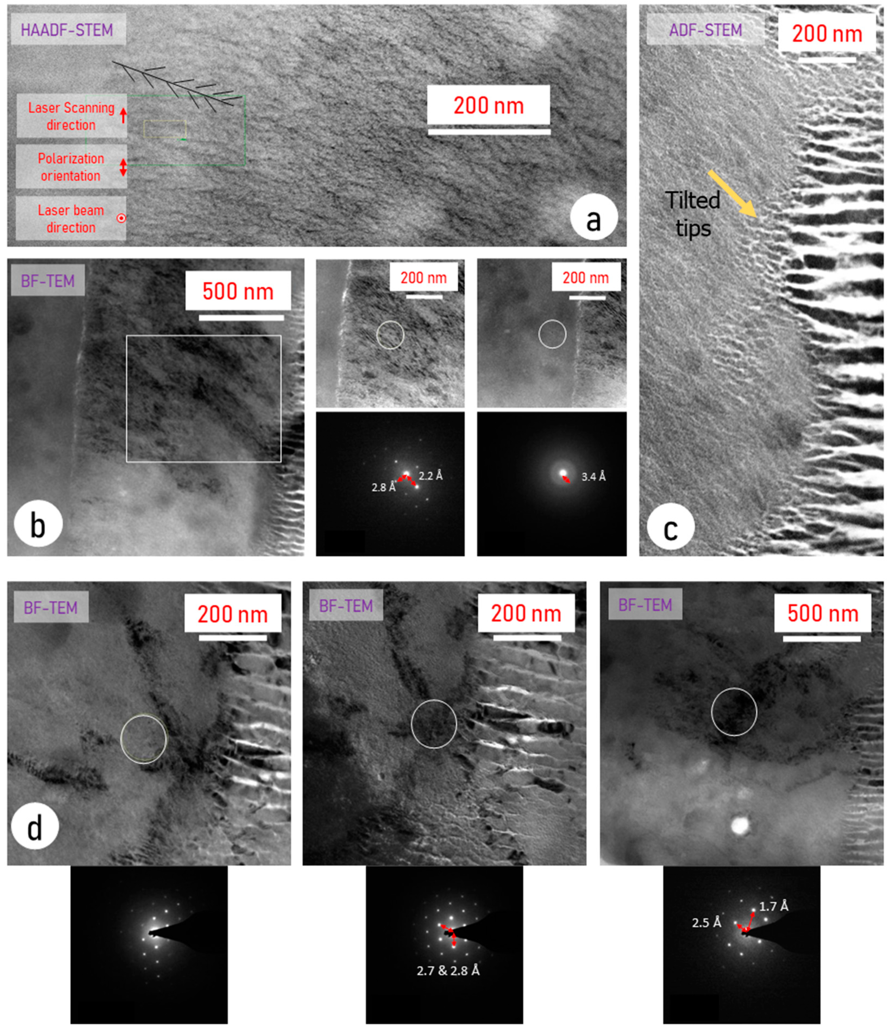
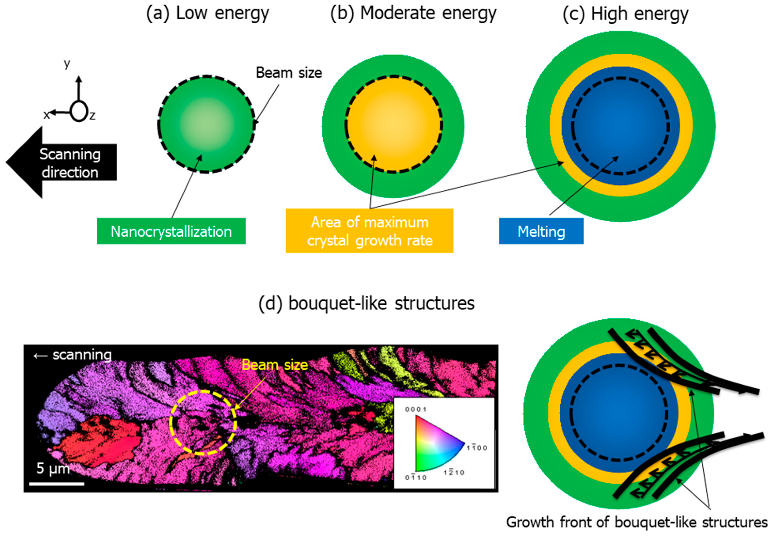
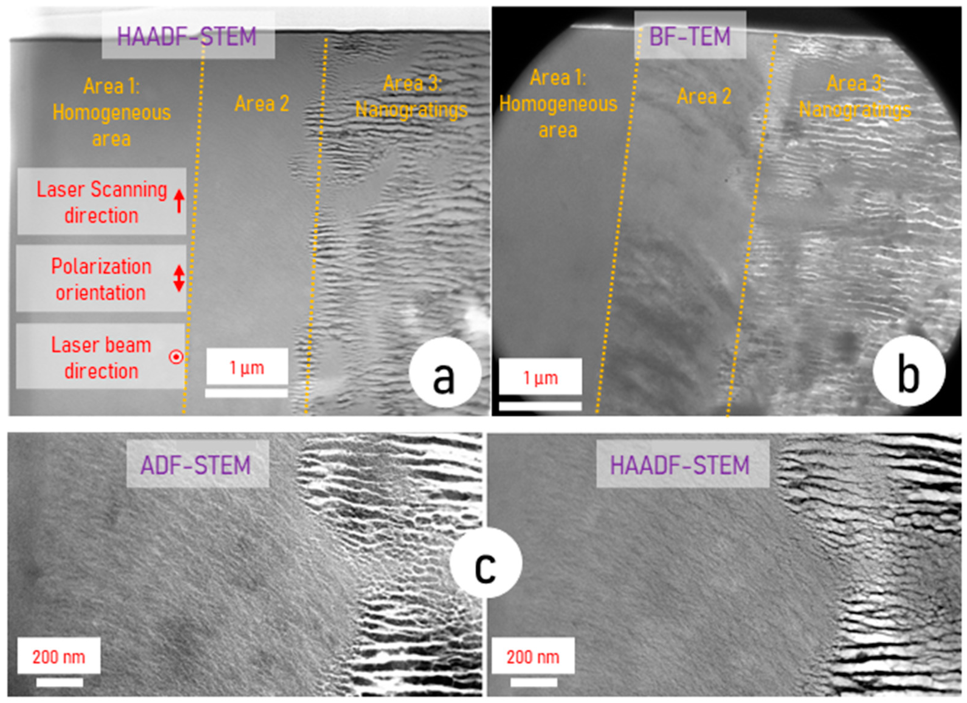
3.1. Nanoscale Structuring and Identification of Laser-Modified Areas

Figure 2 presents HAADF-STEM and BF-TEM observations of the sample slice extracted by FIB. From Figure 2a,b, we can distinguish three distinct areas:
(i)
Area 1 is a heat-affected zone that appears homogeneous in both modes. It does not contain crystallization.
(ii)
Area 2, where there are no nanogratings. The matter has not been exposed to light at this location but has not been melted. Note that the bouquet-like structure is clearly visible in this region as highlighted in Figure 2b.
(iii)
Area 3, where nanogratings are clearly observed, and this region has experienced both irradiation and melting.
It is worth mentioning that there is a fourth area, not visible from Figure 2, corresponding to the pristine glass and different to area 1, as described in [21].
As the HAADF mode is highly sensitive to atomic numbers (inelastic scattering), the heavy elements appear whiter than the light ones. In such a way, we note in Figure 2a that there are dark lines, darker than the rest of the sample, delimiting area 3, revealing regions with a smaller atomic number. This corresponds to pure silica (SiO2) lamellas of the nanogratings. From [21], we know that nanogratings are made of an alternate amount of lamellas composed of amorphous SiO2 and lamellas containing an Nb-rich phase (LiNbO3 phase). The region between lamellas have an Nb content a bit larger than the starting glass. That is why they appear slightly brighter than the glass when the chemical separation is clear enough. This situation is not encountered everywhere in area 3.
Using the BF-TEM mode (Figure 2b), sensitive to electronic thickness and diffraction (the collected electron number is weaker in both cases and thus the intensity is smaller), the lamellas in area 3 that appeared dark in HAADF give rise to white structures. This is in agreement with weaker electron density and/or non-crystalline regions induced by comparatively smaller Nb concentration (SiO2 lamellas).
The regions between the lamellas appear grey due to a higher Nb content and diffraction by LiNbO3 crystals.
In this mode and as opposed to the HAADF mode, we can clearly observe the bouquet structure in area 2 (darker traces akin to leaves similar to those visible in Figure 1), as there is no nanogratings masking them. This contrast does not arise from chemical composition modulation as nothing is visible in HAADF mode. Therefore, we suspect here a contrast due to diffraction (darker means more efficient diffraction in the condition of observation).
The ADF-DTEM micrograph in Figure 2c, sensitive to diffraction and inelastic scattering of light elements, does not show contrast other than that already seen before, i.e., in area 2 thin linear structures (a bit brighter) corresponding to light element accumulation but not crystallized, and in area 3, the lamellas.
Therefore, and also to precisely analyze the nanostructuring at the nanoscale in area 2, the BF mode was used but at a smaller scale, inside and outside the bouquet-like region. The results are reported in Figure 3. Striated contrast in this partly crystallized region in Figure 3a arises from the phase separation from LNS glass into SiO2 and LiNbO3, at least partially. Using BF-TEM, sensitive to diffraction, the organization of this phase separation, seen in Figure 3b, appeared different between the inside and the outside of the bouquet region. One is partly organized in lamellas with a period of ~11.5 ± 1.0 nm (Figure 3b), whereas the other has a tree-like nanostructure. This is clearly observed and schematized in Figure 3a. However, this does not explain the bouquet-like morphology seen in EBSD as the black regions in Figure 3b are wider than the non-indexed region in EBSD. However, by comparing the quality of the crystallization between the dark and the grey regions (Figure 3c), we confirm that both are partially crystallized, but the tilt of the crystal produces a non-symmetric diffraction pattern. This is not the case away from this zone. We thus deduce that orientation disturbance, likely arising from stress accumulation, may lead to difficulty for EBSD to index these specific regions.
Therefore, the bouquet-like traces appearing in EBSD are produced by orientation fluctuation of the LiNbO3 crystallized phase among the phase separation. Performing EBSD in this region showed that the photo-precipitated nanocrystals are less textured inside than outside, as it can be seen in Figure S1.
Additionally, we observe at the “interface” between the nanogratings (area 3) and the striated region (area 2), a morphological transition occurs, as visible from Figure 3d. One can note that the very tips of the nanogratings are tilted so that they tend to align to the striae orientation as exemplified by the yellow arrow in Figure 3d. At the same time, we note that the thickness of the white lamellas (crystalline) decreases, and new lamellas start to appear between them. The plasma structure imposes a larger space separation than the thermal structure. This proves the action of an additional force.
On the other hand, one should expect two sub-areas in the crystallized area 2,one from solid–solid crystallization and one from liquid–solid crystallization, as was described in the introduction. Unfortunately, and as observed in Figure 1c, they are not discernable. However, we suggest that the nucleation of the solid–solid transformation should trigger the second one (liquid–solid), thus orienting the crystallization to, and even through, area 3.
From these observations, we can conclude that the dark zones not indexed in EBSD are crystallized regions and probably badly textured areas, but, in any case, are not non-crystallized areas. From the above reasoning on chemical migration and triggered crystallization, it is now necessary to specify the chemical distribution at the nanoscale within areas 1 to 3, compared to the previous work [21]. EDS and EELS analyses were therefore employed, the latter allowing the monitoring of Li content.

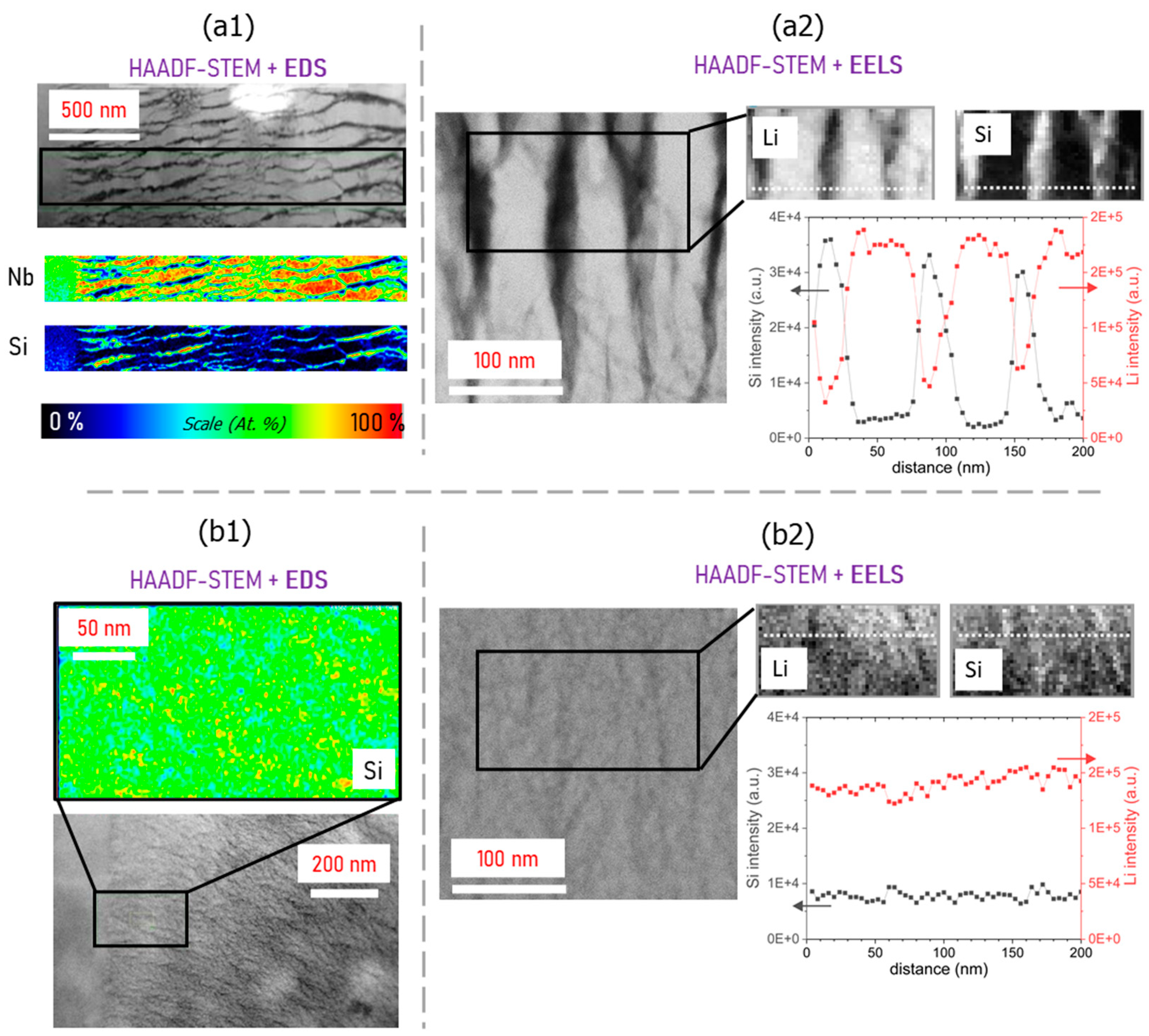
3.2. Chemical Analysis (EDS and EELS) of the Laser-Induced Areas

Following electron microscopy imaging, quantitative chemical analyses (EDS and EELS) were performed in areas 2 and 3 of the sample, i.e., within the nanogratings zone (area 3) and striated regions (area 2). The combination of these techniques was chosen to probe the same area as the Li, Si, and Nb distributions. The results are summarized in Figure 4. In the nanogratings (area 3), EDS analysis revealed at some places a complete chemical separation between Nb and Si, previously observed in [21] (Figure 4(a1)). However, using complementary EELS analysis, we reveal for the first time the chemical concentration of Li during the irradiation process using EELS (Figure 4(b1)). Both Nb and Li elements are found in the Si-poor regions, which is in agreement with the formation of a crystalline LiNbO3–amorphous SiO2 phase separation as previously observed [21].
Based on the pristine glass stoichiometry, the formation of LiNbO3 implies the segregation of pure SiO2, which is well visible from Figure 4(a2). We observe lamellas composed of pure silica and LiNbO3 crystals between them. However, there are some positions still showing the composition of the initial glass. Thus, we can imagine that the glass progressively releases SiO2 attracted towards some lamella-shaped regions. Then, when the glass between the lamellae is impoverished enough in silica content, the material between lamellas is ready to crystallize. Now, turning to the striated region (area 2) seen in Figure 4(b1,b2), chemical elemental mapping revealed an Nb and Li phase separation apart from Si, although with a much lower contrast than the nanograting region. This is consistent with the observation by diffraction patterns (Figure 3b), where the striated region (area 2) was found to contain a larger part of the amorphous phase. Based on the initial glass stoichiometry, a complete chemical separation between SiO2 and crystallized LiNbO3 would yield a volume occupied by ~30% of SiO2 and ~70% of LiNbO3. At the center, the volume fraction of SiO2 is estimated to be ~21% of SiO2 and ~79% of LiNbO3 (calculated based on HAADF-STEM micrographs). This is consistent with a quasi-complete chemical separation between the two phases at the center. However, as can be observed in Figure 4a from the EDS-STEM analysis, there is still some residual glass inside the nanogratings, which would explain the slightly lower SiO2/LiNbO3 volume ratio measured. The magnitude of the elemental chemical separation is also different when comparing the nanograting (area 3) and the striated regions (area 2). For the former, and at the center of the laser track, the normalized atomic percentage Nb/Si goes from 90/10 in the crystalline area (formation of LiNbO3) down to ~5/95 in the amorphous region. For the striated region, the evolution of this Nb/Si ratio goes from ~70/30 to ~60/40. When looking at the amorphous region, the Nb/Si ratio oscillates around ~65/35, which is close to the expected pristine glass stoichiometry (i.e., 67/33).
Finally, when moving from the laser track center and towards the edge (interface between areas 2 and 3), the nanogratings periodicity diminishes (from ~125 nm to ~50 nm). Since the plasma density is lower in the outer beam waist area, less elemental migration is also expected [22,23]. This appears as the phase separation between LiNbO3 and SiO2 is not “completed” at the interface between areas 2 and 3.

4. Discussion

From the above observations, it is now possible to answer the questions developed in the introduction.
First, the origin of the bouquet-like structure is likely a combination of both small crystallized domains (a few nm in size) mixed with an amorphous phase, and poor indexing quality by EBSD, resulting in the impossibility to define the orientation in this region. EBSD analysis can thus lead to confusing results. The dark zones (such as in Figure 1c) are not completely amorphous areas, but the phase separation with the crystallized part is poorly textured. This can be seen in Figure 5, where the same EBSD images are displayed but with parameters used in the post-data treatment changed (dilation and confidence index [24]). More specifically, by modifying from a confidence index 0.2 and cleaning dilation of 33, to a confidence index of 0.05 and no cleaning dilation, almost the whole laser-affected region appears crystallized. The bouquet-like structure is thus constituted of crystalline areas with insufficient quality indexation. This is also clearly visible in the IQ image provided in the Supporting Materials section.
To continue the discussion on the bouquet-like structures, it is also found that they are laser polarization independent. This shows that their origin does not occur in the irradiated volume, unlike nanogratings. As suggested in [14] (Section 4.2.4), the crystal front growth is backward and starts from the periphery (Figure 1c). Complementarily, the bouquets are independent with respect to nanogratings structuring since the latter is oriented by the laser polarization. Thus, we understand that the bouquets can cross the nanogratings without disturbing them. It can be thus deduced that the observed chemical separation in the irradiated region is produced before any crystallization and is influenced by the plasma spatial structuration. Then, when the separation is large enough, the material between the silica-rich lamellae may eventually crystallize.
The structuring of the chemical separation into thin lamella made of silica glass with larger separation in the irradiated area than in the non-irradiated area proves that the electron plasma induced during laser irradiation plays a role in it. For example, the lamella period varies at the interface between areas 2 and 3 (Figure 3), marking the limit between the light deposition and the non-irradiated area.
The next question is: how does the plasma impose its structuring on the chemical separation? In [25], the physical origin of the nanogratings in silica, that are made of nanopores arranged in quasi-periodic nanoplans, is the nucleation of nanopores and cavitation. This process is coupled to electromagnetic waves through temperature modulations perpendicular to the laser polarization induced by electron plasma energy transfer to the lattice. There is no chemical diffusion in this scenario but a destabilization of SiO2 at the place of high electron density where the energy deposition is thus the largest. Here, from the results presented in this paper, we suggest an alternative picture to the observed chemical separation. Instead, we propose that the plasma imprints its spatial structure on the chemical separation achievement through electrochemical potential leading to the uniformity of the Gibbs energy. At the ultrashort time scale, the space modulation of the excited electron density under light influence is recognized as being trapped into the glass and re-excited by the next pulse, thus reinforcing the nanograting structure. If the plasma structure is achieved during a first pulse of a few 0.1 ps, 10 to 100 pulses are necessary for building a nanograting in pure silica, for example [26]. This mechanism plays a memory role in the plasma structure and thus may develop transformations on a much longer time scale than during a single pulse duration. We suggest that the mechanism here starts similarly. However, we notice that if the starting excitation follows the light intensity profile, this is no longer the case after several pulses. This means that positive ions produced at the beginning and negative ions produced by the electron trapping do not have the same distribution, yielding to an electric field modulation along the laser polarization direction. A simple classical calculation leads to a saw-tooth shape curve with an amplitude that could reach several volts per µm considering an excited electron density of 1019 e/cm3 [22,27,28]. Such a large field has to be taken into account in the physico-chemical processes. Here, there are two aspects of interest in the present observations. The first is the involvement of the electric field in the phase separation. The second aspect is the migration of species in an electric field. Although it is not the place here for detailing the theory, we can show that phase separation is guided by the gain in free energy that is the sum
G = i n i μ ˜ i
where ni are the number of particles i, and μ ˜ i the electrochemical potential expression (see for instance [29]). In a pure electrostatic problem, we can consider the following expression
μ ˜ i = μ i + z i ϕ + 1 2 ε 0 ( ε r , i 1 ) E 2 x i v i
with μ i the chemical potential, z i the charge of the species I, the faraday constant, ϕ the electric potential, ε r , i the partial relative permittivity, E the electric field, x i the molar fraction, and v i the partial molar volume.
As the partial relative permittivity can be different for each species, we understand that phase separation can be influenced by E, resulting in a net separation. The migration of species is easy to understand when they are ionic because it is the classical coulombian force that comes into play, but when there are no ionic species such as for SiO2 groups, the force is more complex. On that point, we have to consider the principle that migrations are under forces introduced by the gradient of electrochemical potentials. As a matter of fact, starting from a homogeneous glass, the introduction of space charge and a related electric field perturbates this homogeneity. A new equilibrium is reached, in which the different electrochemical gradients compensate through expressions that are well known in the thermodynamics of irreversible phenomena, i.e., flux cancelling such that
J i = j L i j μ ˜ j ,
where Lij are the Onsager coefficients.
We suggest that this process drives the silica migration that accumulates at the place of high electron density, that is where the electric field is vanishing and where the electric potential is at maximum. In turn, pure silica lamellas, extracted from the glass, will develop. The chemical composition of the remaining glass is therefore impoverished in silica, and, after a while, is ready for crystallization. Then, the texturing of the crystallization is induced by the peripheral solid–solid crystallization for the parameter domain investigated here as described at the beginning of the paper.
In such a model, there is, thus, an additional force, an electrochemical one, that is super-imposed to the thermal force (thermodynamical phase separation), which leads to a quasi-period of the chemical nanogratings being larger than those observed under simple thermal treatment. This is most likely of the same nature of the process observed in [23].

5. Conclusions

In this work, we clarify the origin of bouquet-like structures that were observed in LNS glasses, using a combination of high-resolution electron microscopy techniques and chemical analyses. The observed bouquet-like structure arises from poorly textured crystals during the crystallization process that starts from the periphery of the heat-affected zone. The typical formation of nanogratings, which are laser polarization dependent, are neither structurally, nor compositionally, perturbated by the crossing of the bouquet “leaves”. This is because chemical separation is initiated before the crystallization under the influence of the excited electron plasma structure. This points out a different mechanism than that working in pure silica for which transformations leading to nanogratings’ achievement are made without chemical migration. We suggest that the electronic plasma, being self-organized, produces modulated driving forces from the modulation of the electrochemical potential of the glass constituents.

Supplementary Materials

The following supporting information can be downloaded at: https://www.mdpi.com/article/10.3390/cryst12040496/s1, Figure S1. EBSD part of the picture in Figure 1d: Image quality (IQ) map, and inverse pole figure (IPF) with CI = 0.33 and cleaning dilation = 33, color coding as in Figure 1d. Figure S2. Description of the setup in three steps: 1—a slice is extracted by FIB; 2—the slice is subsequently placed on a TEM grid and thinned down to ~100 nm thickness; 3—the prepared slice is subsequently investigated by electron microscopy. References [10,20,28,29] are cited in the Supplementary Materials.

Author Contributions

Conceptualization, M.C. and B.P.; methodology, B.P.; validation, M.C., B.P., and M.L.,; formal analysis, M.V.; investigation, M.C., J.C., F.B., M.V., L.M.; resources, B.P., M.L., M.C.; writing—original draft preparation, M.C., B.P., M.L., M.V., B.D.; writing—review and editing, M.C., B.P., M.L., M.V., B.D., F.B., J.C.; visualization, M.C., B.P; supervision, B.P.; project administration, M.C., B.P.; funding acquisition, M.C., B.P., M.L. All authors have read and agreed to the published version of the manuscript.

Funding

This work was supported by the French National Research Agency under the program CHARMMMAT ANR-11-LABX-0039-grant. Electron microscopy was carried out within the MATMECA project supported by the ANR under contract number ANR-10-EQPX-37.

Institutional Review Board Statement

Nt applicable.

Informed Consent Statement

Nt applicable.

Data Availability Statement

Data available upon reasonable request from the authors.

Conflicts of Interest

The authors declare no conflict of interest.

References

  1. Komatsu, T. Design and control of crystallization in oxide glasses. J. Non-Cryst. Solids 2015, 428, 156–175. [Google Scholar] [CrossRef]
  2. Maksimova, O.S.; Korzunova, L.V.; Milberg, Z.P. Properties and structure of glasses of the system Li2O-Nb2O5-SiO2. Izv. Akad. Nauk Latv. SSR Ser. Khim 1975, 5, 530–534. [Google Scholar]
  3. Yonesaki, Y.; Miura, K.; Araki, R.; Fujita, K.; Hirao, K. Space-selective precipitation of non-linear optical crystals inside silicate glasses using near-infrared femtosecond laser. J. Non-Cryst. Solids 2005, 351, 885–892. [Google Scholar] [CrossRef]
  4. Sigaev, V.N.; Golubev, N.V.; Stefanovich, S.Y.; Komatsu, T.; Benino, Y.; Pernice, P.; Aronne, A.; Fanelli, E.; Champagnon, B.; Califamo, V.; et al. Second-order optical non-linearity initiated in Li2O–Nb2O5–SiO2 and Li2O–ZnO–Nb2O5–SiO2 glasses by formation of polar and centrosymmetric nanostructures. J. Non-Cryst. Solids 2008, 354, 873–881. [Google Scholar] [CrossRef]
  5. Vigouroux, H. Etude de Vitrocéramiques Optiques Pour le Doublement de Fréquence in Sciences Chimiques; University of Bordeaux: Bordeaux, France, 2012; p. 278. [Google Scholar]
  6. Dai, Y.; Zhu, B.; Qiu, J.R.; Ma, H.L.; Lu, B.; Yu, B.K. Space-selective precipitation of functional crystals in glass by using a high repetition rate femtosecond laser. Chem. Phys. Lett. 2007, 443, 253–257. [Google Scholar] [CrossRef]
  7. Gerth, K.; Rüssel, C.; Keding, R.; Schleevoigt, P.; Dunken, H. Oriented crystallisation of lithium niobate containing glass-ceramic in an electric field and determination of the crystallographic orientation by infrared spectroscopy. Phys. Chem. Glasses 1999, 40, 135–139. [Google Scholar]
  8. Veenhuizen, K.; McAnany, S.; Nolan, D.; Aitken, B.; Dierolf, V.; Jain, H. Fabrication of graded index single crystal in glass. Sci. Rep. 2017, 7, 44327. [Google Scholar] [CrossRef] [Green Version]
  9. Shimada, M.; Honma, T.; Komatsu, T. Laser patterning of oriented LiNbO3 crystal particle arrays in NiO-doped lithium niobium silicate glasses. Int. J. Appl. Glass Sci. 2018, 9, 518–529. [Google Scholar] [CrossRef]
  10. Cao, J.; Poumellec, B.; Mazerolles, L.; Brisset, F.; Helbert, A.-L.; Surble, S.; He, X.; Lancry, M. Nanoscale Phase Separation in Lithium Niobium Silicate Glass by Femtosecond Laser Irradiation. J. Am. Ceram. Soc. 2016, 100, 115–124. [Google Scholar] [CrossRef] [Green Version]
  11. Fan, C.; Poumellec, B.; Lancry, M.; He, X.; Zeng, H.; Erraji-Chahid, A.; Liu, Q.; Chen, G. Three-dimensional photoprecipitation of oriented LiNbO3-like crystals in silica-based glass with femtosecond laser irradiation. Opt. Lett. 2012, 37, 2955–2957. [Google Scholar] [CrossRef] [PubMed]
  12. Weis, R.S.; Gaylord, T.K. Lithium niobate: Summary of physical properties and crystal structure. Appl. Phys. A 1985, 37, 191–203. [Google Scholar] [CrossRef]
  13. Choy, M.M.; Byer, R.L. Accurate second-order susceptibility measurements of visible and infrared nonlinear crystals. Phys. Rev. B 1976, 14, 1693–1706. [Google Scholar] [CrossRef]
  14. Cao, J.; Lancry, M.; Brisset, F.; Mazerolles, L.; Saint-Martin, R.; Poumellec, B. Femtosecond Laser-Induced Crystallization in Glasses: Growth Dynamics for Orientable Nanostructure and Nanocrystallization. Cryst. Growth Des. 2019, 19, 2189–2205. [Google Scholar] [CrossRef]
  15. Rajeev, P.P.; Gertsvolf, M.; Hnatovsky, C.; Simova, E.; Taylor, R.S.; Corkum, P.B.; Rayner, D.M.; Bhardwaj, V.R. Transient nanoplasmonics inside dielectrics. J. Phys. B At. Mol. Opt. Phys. 2007, 40, S273–S282. [Google Scholar] [CrossRef]
  16. Kazansky, P.G. Formation of Sub-wavelength Periodic Structures Inside Transparent Materials. In 3D Laser Microfabrication; Misawa, H., Juodkazis, S., Eds.; Wiley-VCH Verlag GmbH & Co., KGaA: Weinheim, Germany, 2006; pp. 181–198. [Google Scholar]
  17. Fan, C. Directional Writing Dependence of Birefringence in Multicomponent Silica-based Glasses with Ultrashort Laser Irradiation. J. Laser Micro Nanoeng. 2011, 6, 158–163. [Google Scholar] [CrossRef]
  18. Cao, J.; Poumellec, B.; Brisset, F.; Helbert, A.-L.; Lancry, M. Angular Dependence of the Second Harmonic Generation Induced by Femtosecond Laser Irradiation in Silica-Based Glasses: Variation with Writing Speed and Pulse Energy. World J. Nano Sci. Eng. 2015, 5, 96–106. [Google Scholar] [CrossRef] [Green Version]
  19. Müller, R.; Zanotto, E.; Fokin, V.M. Surface crystallization of silicate glasses: Nucleation sites and kinetics. J. Non-Cryst. Solids 2000, 274, 208–231. [Google Scholar] [CrossRef]
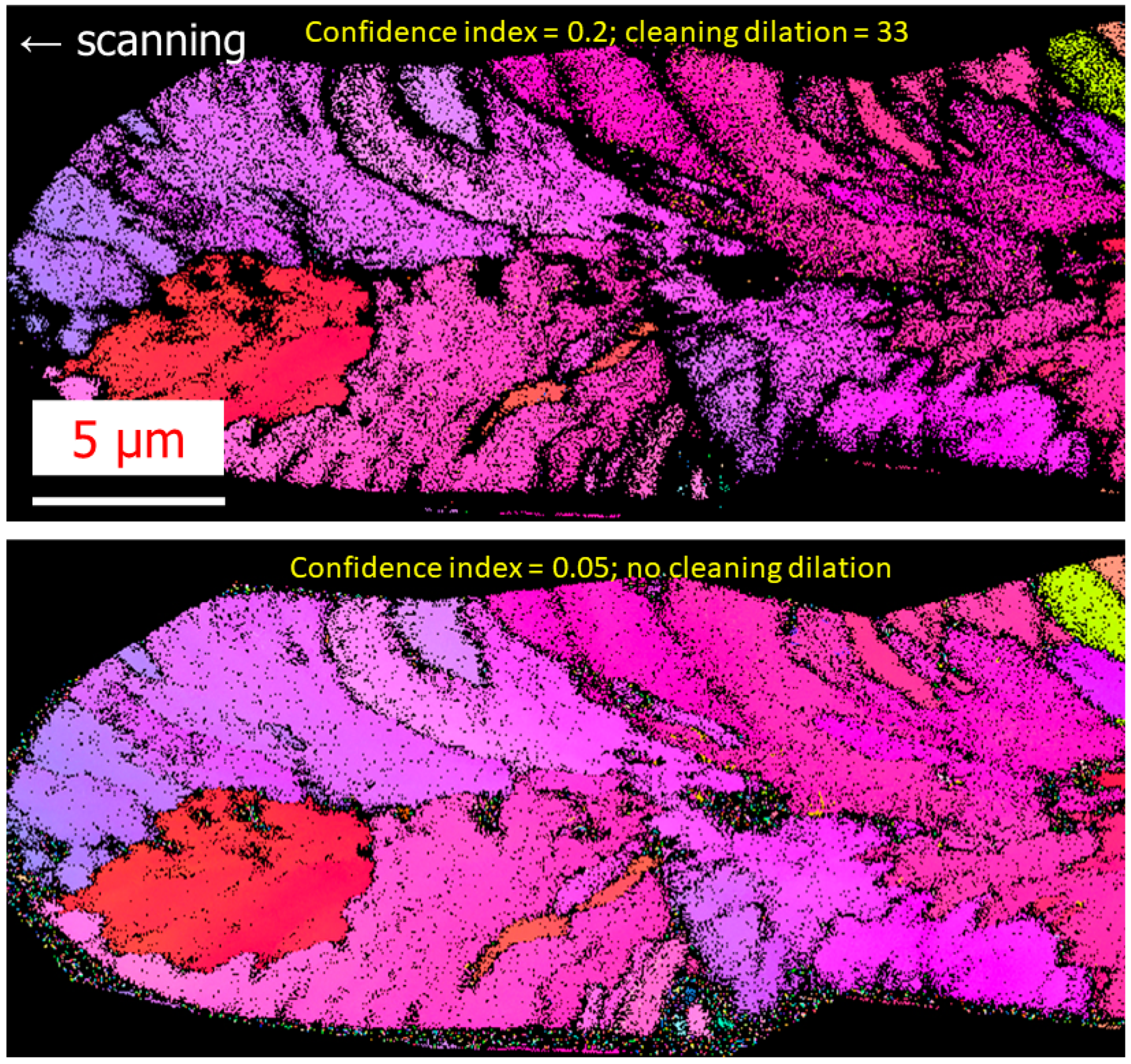
  20. Wright, S.I.; Nowell, M.M. EBSD Image Quality Mapping. Microsc. Microanal. 2006, 12, 72–84. [Google Scholar] [CrossRef] [PubMed]
  21. Cao, J.; Mazerolles, L.; Lancry, M.; Brisset, F.; Poumellec, B. Modifications in lithium niobium silicate glass by femtosecond laser direct writing: Morphology, crystallization, and nanostructure. J. Opt. Soc. Am. B 2016, 34, 160. [Google Scholar] [CrossRef]
  22. Fernandez, T.T.; Sakakura, M.; Eaton, S.; Sotillo, B.; Siegel, J.; Solis, J.; Shimotsuma, Y.; Miura, K. Bespoke photonic devices using ultrafast laser driven ion migration in glasses. Prog. Mater. Sci. 2018, 94, 68–113. [Google Scholar] [CrossRef]
  23. Fernandez, T.T.; Siegel, J.; Hoyo, J.; Sotillo, B.; Fernández, P.; Solis, J. Controlling plasma distributions as driving forces for ion migration during fs laser writing. J. Phys. D Appl. Phys. 2015, 48, 155101. [Google Scholar] [CrossRef] [Green Version]
  24. Brewer, L. Risks of “Cleaning” Electron Backscatter Diffraction Data. Microsc. Today 2010, 18, 10–15. [Google Scholar] [CrossRef] [Green Version]
  25. Rudenko, A.; Colombier, J.; Itina, T.E.; Stoian, R. Genesis of Nanogratings in Silica Bulk via Multipulse Interplay of Ultrafast Photo-Excitation and Hydrodynamics. Adv. Opt. Mater. 2021, 9, 2100973. [Google Scholar] [CrossRef]
  26. Desmarchelier, R.; Poumellec, B.; Brisset, F.; Mazerat, S.; Lancry, M. In the Heart of Femtosecond Laser Induced Nanogratings: From Porous Nanoplanes to Form Birefringence. World J. Nano Sci. Eng. 2015, 5, 115–125. [Google Scholar] [CrossRef] [Green Version]
  27. Couairon, A.; Sudrie, L.; Franco, M.; Prade, B.; Mysyrowicz, A. Filamentation and damage in fused silica induced by tightly focused femtosecond laser pulses. Phys. Rev. B 2005, 71, 125435. [Google Scholar] [CrossRef]
  28. Huang, F.; Si, J.; Chen, T.; Shen, T.; Shi, M.; Hou, X. Temporal-spatial dynamics of electronic plasma in femtosecond laser induced damage. Opt. Express 2021, 29, 14658–14667. [Google Scholar] [CrossRef] [PubMed]
  29. Han, G.; Wang, H. Generalized expression of chemical potential with influence of external fields and its applications: Effect of charged particles on droplet condensation. Fluid Phase Equilib. 2013, 338, 269–273. [Google Scholar] [CrossRef]
Figure 1. (a) A regime of nanogratings’ crystallization, with orientation controlled by light polarization; (b) a regime with a maximized growth rate at the center; (c) a regime where part of the irradiated region is melted; (d) the growth rate upon scanning yields to the formation of bouquet-like structures (adapted from [14]). Additional details on experimental work: fs laser-induced nanostructures (LiNbO3 seen by EBSD coded, on the base of R3c space group, in the direction of laser propagation) in 32.5%Li2O-27.5%Nb2O5-40%SiO2 (mol%) glass, laser wavelength 1030 nm, pulse duration 300 fs, pulse frequency 500 kHz, scanning speed 5 µm/s, and focus 450 μm below the surface with a pulse energy at 1.8 μJ. The color code indicates the crystal direction along writing laser propagation direction. Dark regions are opened from the center to the periphery as with a bouquet oriented towards the writing direction. The laser beam size (yellow circle) is one-third of the written line width.
Crystals 12 00496 g001
Figure 2. Electron micrographs of LNS sample irradiated by fs laser and investigated using a TITAN3 G2 TEM. (a) HAADF-STEM mode, (b) BF-TEM mode, and (c) magnification on Area 2 using ADF-STEM mode and HAADF-STEM mode.
Crystals 12 00496 g002
Figure 3. (a) HAADF-STEM of area 2 and out of bouquet structures, (b) BF-TEM and diffraction patterns of both areas 2 and 1 inside the region of the bouquet, (c) ADF-STEM at the interface between areas 2 and 3, and (d) BF-TEM and diffraction patterns in area 2, between dark and brighter regions The reference frame (laser scanning direction, polarization orientation, etc., is identical to Figure 2).
Crystals 12 00496 g003
Figure 4. Chemical analysis using EDS technique on (a1) nanogratings (area 3) and (b1) striated (area 2) + homogeneous regions (area 1); chemical analysis using EELS technique on (a2) nanogratings and (b2) striated regions (areas 3 and 2, respectively). In (a2,b2), the graphs correspond to the intensity modulation extracted from EELS along the direction represented by the dotted white line.
Crystals 12 00496 g004
Figure 5. Comparison between two EBSD pictures but with smaller confidence index and with/without cleaning procedures using OIMTM software.
Crystals 12 00496 g005
Publisher’s Note: MDPI stays neutral with regard to jurisdictional claims in published maps and institutional affiliations.

