Introduction
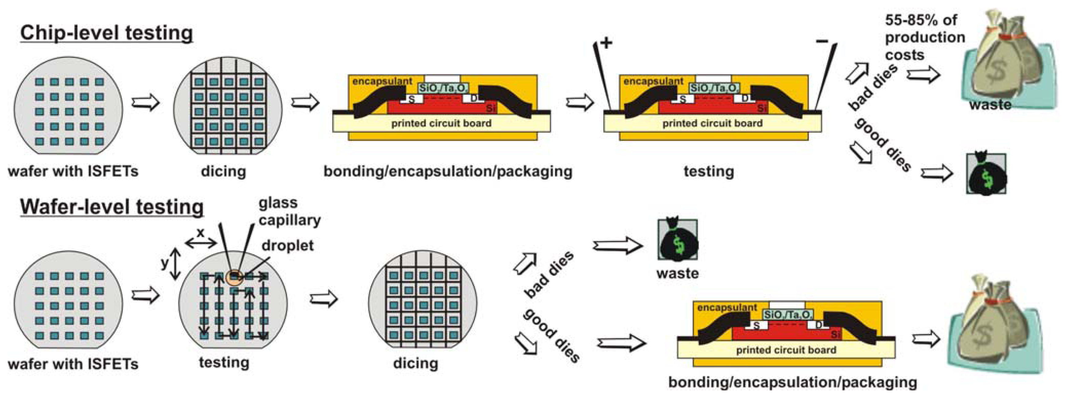
Today, although well-established microelectronic mass-production techniques are used for the fabrication of microsensors and microsystem components, prices are still high. This is at least partly due to the fact that up to now the quality control and testing of microsensors and microsystem components is often carried out on chip-level, i.e. after dicing, bonding, encapsulation and mounting processes. This is an uneconomical approach, because the interconnection, encapsulation and packaging costs for microsystems can be very high, typically in the order of 55-85% of the total production costs [
1,
2]. These costs are further wasted for non-functioning chips (bad dies, see
Figure 1). Therefore, testing at wafer level should be preferred in order to identify defects (shorted conducting paths, physically destroyed layers, conductor break, etc.) and to select those devices, which meet the predefined quality at the earliest stage (good dies), and thus, to avoid further expensive processes for bad dies (
Figure 1). In the production of integrated circuits, the testing and quality control at wafer level is an established technology; different automatic wafer probers and testers are commercially available (see, e.g. [
3]). Recently, wafer-level test solutions for several physical sensors, like pressure sensors, accelerometers and microphones, have been presented, too [
4].
On the other hand, there is an increasing demand for (bio-)chemical sensors and microanalysis systems such as μTAS (micro total analysis system), lab-on-a-chip and electronic-tongue devices with a wide field of possible applications ranging from medicine, biotechnology and environmental monitoring over food and drug industries to defence and security purposes including antibioterrorism and biological warfare-agents field. Wafer-level testing of electrochemical microsensors, in particular ISFETs (ion-sensitive field-effect transistor) is much more difficult, because a non-electrical external stimulus such as liquid chemical substances should be applied to the gate of this device in order to verify its functionality. At the same time, the bonding pads or contact areas for electrical testing should be kept dry and isolated from the electrolyte solution. Minute electrolyte droplets could be dispensed (e.g., manually or using an ink-jet system) on the wafer in the gate region of the respective ISFET under test. Such a technique in combination with appropriate electrochemical techniques (e.g., cyclic voltammetry, electrochemical impedance spectroscopy and scanning electrochemical impedance spectroscopy) has been utilised for wafer-level quality control of microelectrodes [
5]. In addition, a gel-based wafer-level testing procedure for microelectrodes has been suggested in [
2]. However, due to the small gate sizes of ISFETs, special techniques are needed to reproducibly produce and control small droplets of a test sample. A capillary microcell [
6,
7], which is put directly onto the surface of interest (see
Figure 2), could be a very useful technique to position tiny electrolyte droplets on the investigated surface and to provide spatially resolved electrochemical measurements on wafer level and in the micrometer scale.
In this work, we report on the development and application of a specifically designed capillary electrochemical micro-droplet cell in combination with a commercial wafer prober-station to realise a wafer-level functionality testing and characterisation system for ISFET devices.
Experimental
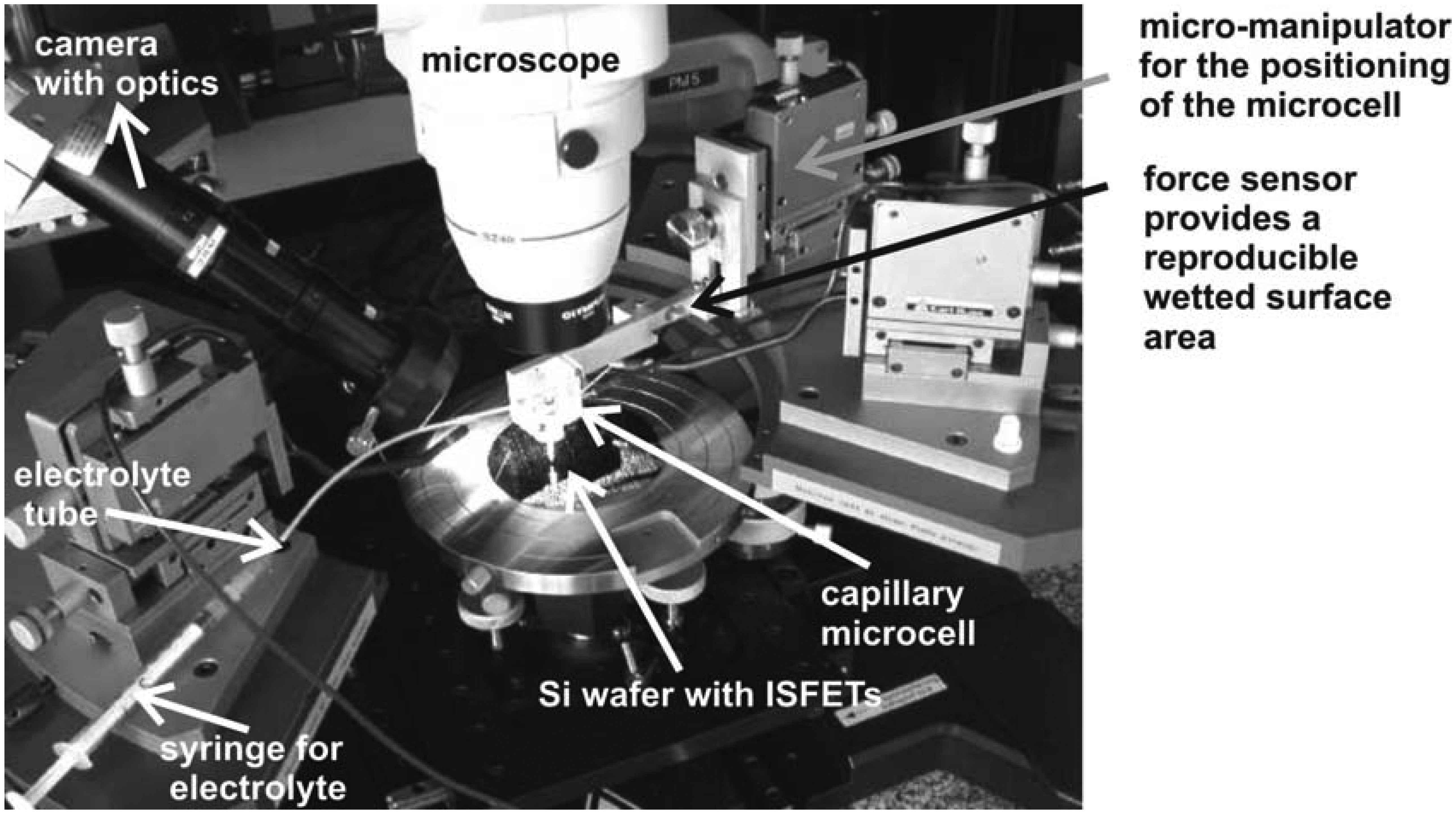
The developed wafer-level testing system for ISFETs is shown in
Figure 3. It combines the following basic parts: A commercial wafer prober-station (PM5 from Süss Microtec), a capillary micro-droplet cell, a semiconductor parameter analyzer (4155C from Agilent) or home made 4-channel ISFET-meter (not shown), a micromanipulator for the positioning of the microcell, and a microscope for optical control. An additional video microscope is used to control the droplet size, the contact between the surface and the filled glass capillary, and the position of the capillary onto the gate region. A constant mechanical contact pressure and thus, a reproducible wetted surface area has been achieved using a force sensor (KD45 from ME-Messsysteme GmbH, Germany), which monitors the force between the capillary tip and the wafer surface, digitizes the value and transfers it to the computer [
6,
7]. The computer can check whether the capillary is in contact with the wafer or not.
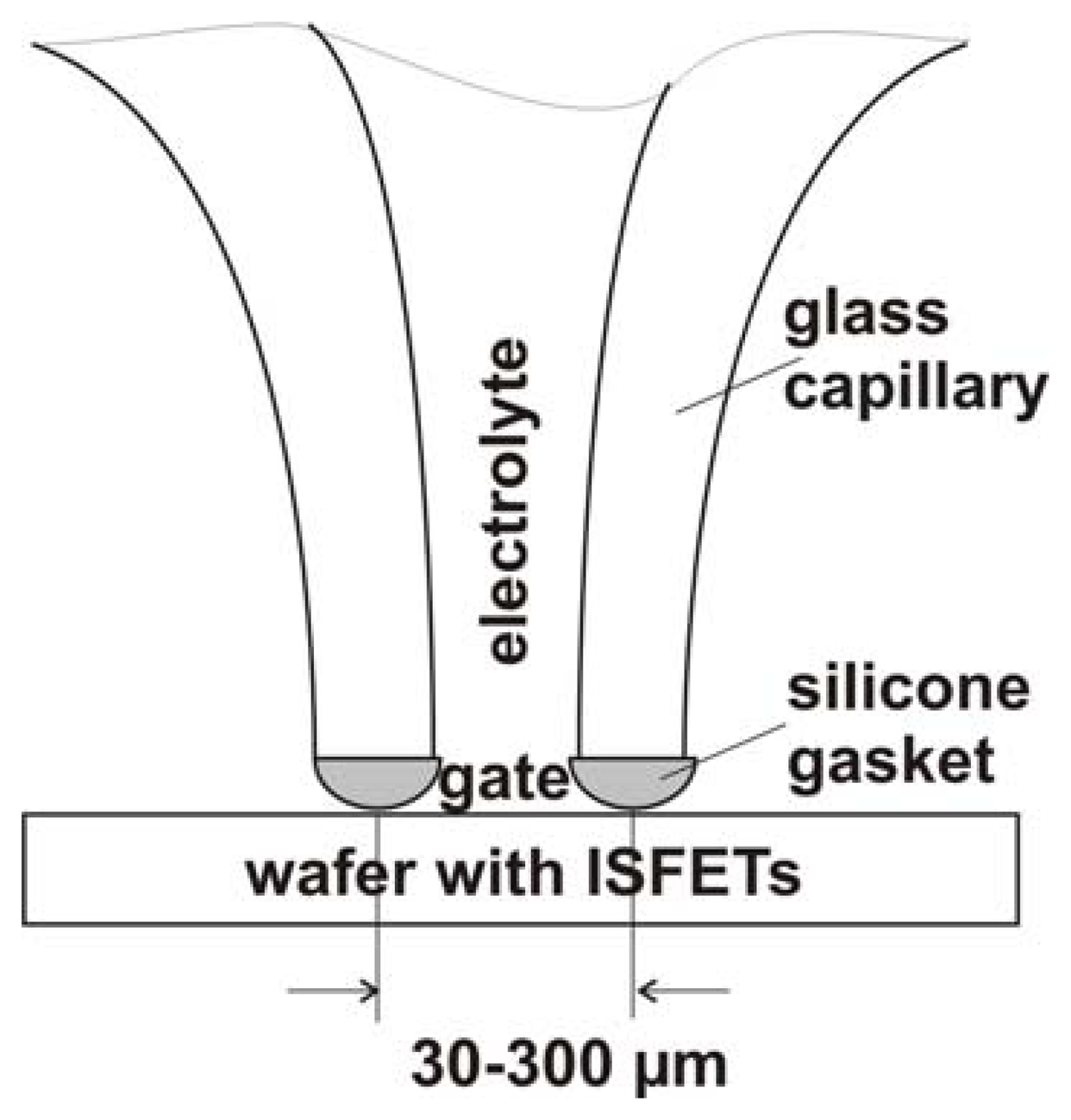
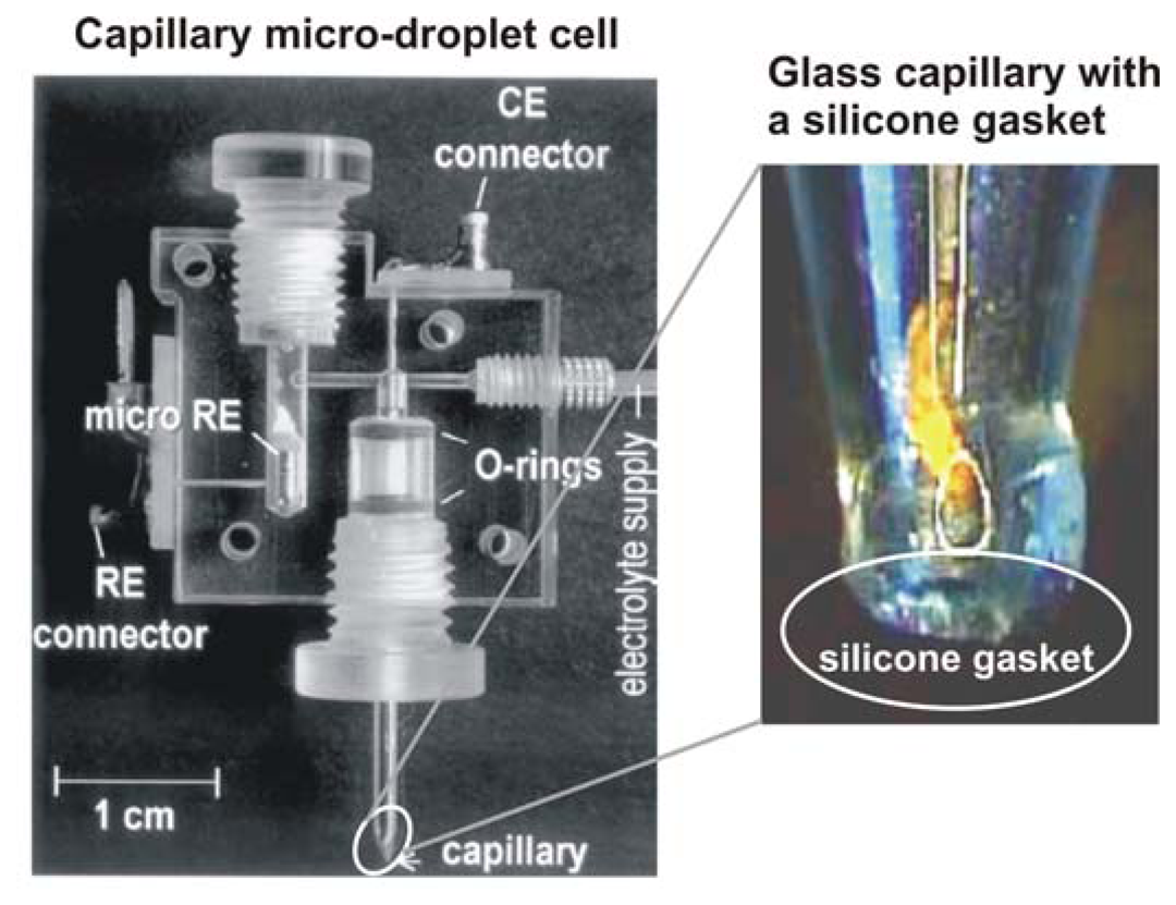
The designed capillary micro-droplet plexiglass-cell is based on a conventional three-electrode arrangement (
Figure 4). The reference (Au wire or Hg/HgCl
2) and counter (Au wire) electrodes are connected by the glass capillary filled with the electrolyte. A silicone gasket has been formed on the flat glass-capillary tip, which has been prepared by previous laser pulling and mechanical polishing. The hydrophobic surface of the silicone gasket prevents leakage of the electrolyte. Prior to measurements, a droplet of an electrolyte solution is applied on the die under test, exclusively covering the gate region of the respective ISFET. The contact area of the gate with the electrolyte is defined by the diameter of the silicone gasket. Because of the adjustable geometry of the tip size of the capillary, the rest of the ISFET has no contact to the electrolyte.
Results and discussion
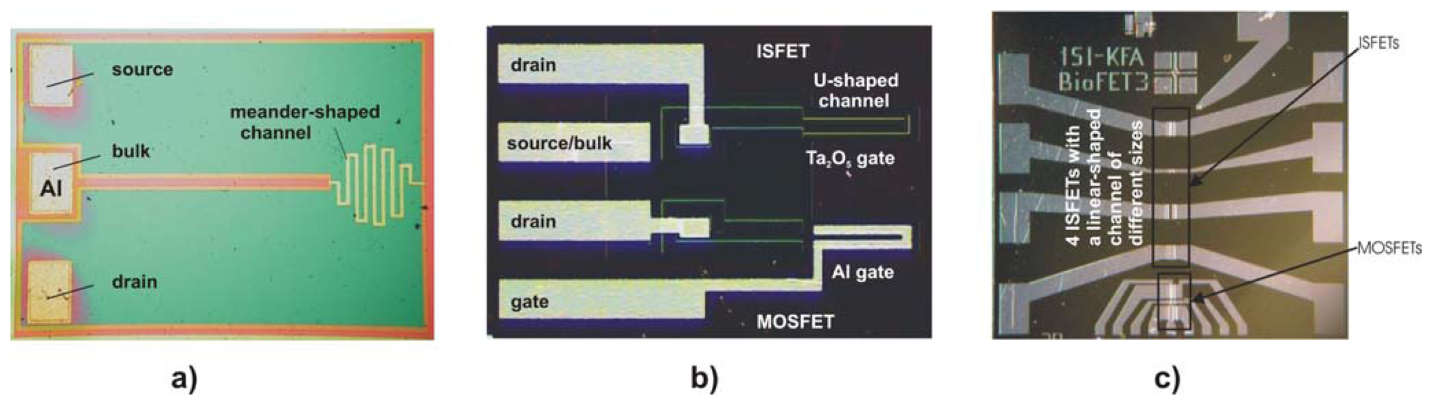
The system has been tested using wafers combining n-channel ISFETs with different geometrical sizes and gate layouts (linear-, meander- and U-shaped). The layouts of the ISFETs used are presented in
Figure 5. The double-layer gate insulator consists of SiO
2 (80 nm)/Ta
2O
5 (80 nm) (layout (a) and (b)) and SiO
2 (30 nm)/Si
3N
4 (70 nm) (layout (c)) films. The pH-sensitive Ta
2O
5 and Si
3N
4 layers have been prepared by thermal oxidation of sputtered Ta (40 nm thick) in a dry oxygen atmosphere for about 2 h and PECVD (plasma-enhanced chemical vapour deposition) method, respectively. The basic characteristics of these ISFETs (but encapsulated) have been reported previously (see e.g., [
8-
10]).
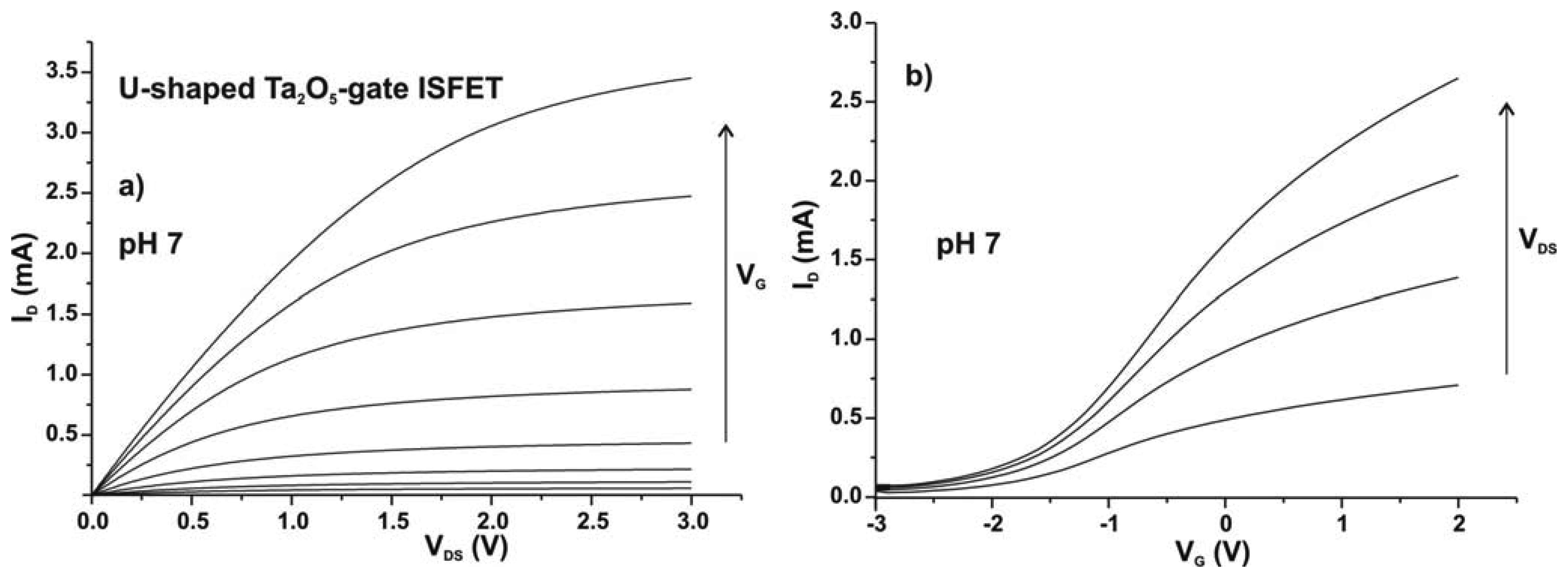
To test the functionality of the ISFETs, a buffer droplet of pH 7 was applied to the gate area of the selected ISFET on the wafer by means of the micro-droplet cell, and a set of output and transfer curves has been recorded using a semiconductor parameter analyzer or a home-made ISFET-meter. Dependent on the ISFET layout and the size of the gate area (see
Figure 5), capillaries with different diameters have been used. As an example,
Figure 6 exemplarily shows a typical set of output (a) and transfer (b) curves of a U-shaped Ta
2O
5-gate ISFET (layout (b) in
Figure 5). They are comparable to those that have been measured on chip-level with fully encapsulated ISFETs, i.e. after the complete fabrication process.
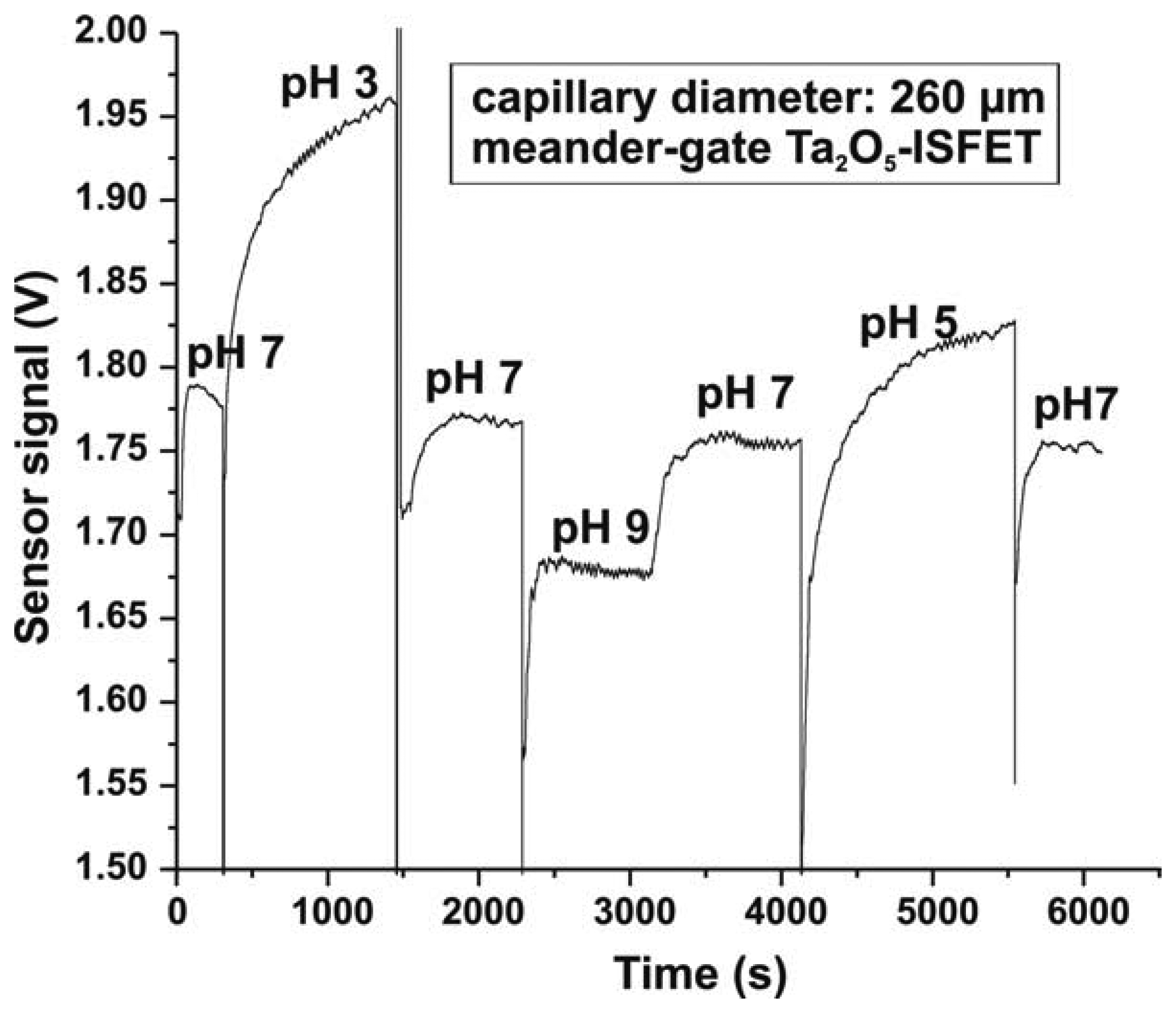
In addition to functionality tests, the developed system allows also a wafer-level characterisation of ISFETs in terms of pH sensitivity or hysteresis by applying buffer droplets with different pH values to the gate surface. Prelimanary experiments have verified the possibility to perform such measurements with the developed micro-droplet cell. As an example,
Figure 7 represents a constant-charge-mode dynamic response for a meander-shaped Ta
2O
5-gate ISFET (layout (a) in
Figure 5) in buffer solutions of different pH values from pH 3 to pH 9 measured on wafer level by means of the developed experimental set-up with the micro-droplet cell. The pH sensitivity evaluated from
Figure 7 was about 50 mV/pH (in comparison to 55-58 mV/pH for the encapsulated Ta
2O
5-ISFET [
8]). At the same time, a relatively large hysteresis and a longer response time have been observed that can be attributed to rests of the previous buffer solution due to difficulties of careful rinsing of the capillary and the ISFET-gate surface as well as due to the possible presence of micro-bubbles in the gate region. These disadvantages could be avoided by using a flow-through capillary micro-droplet cell, which has been recently proposed in [
7]. Here, a continuous electrolyte flow might allow an easy and careful rinsing of the micro-droplet cell and the gate surface as well as a faster change of different pH buffer solutions.
An ISFET is one of the basic structural elements of a new generation of chemical sensors and biosensors. At present, ISFET-based sensors and sensor arrays have been successfully realised for the detection of pH, concentration of different ions and analytes as well as for the measurement of even action potentials of living cells (see, e.g., review [
11]). Recently, several attempts have been also made to apply field-effect transistors for the detection of macromolecular interactions such as antibody-antigen binding, DNA (deoxyribonucleic acid) hybridisation, etc. [
12-
14]. In addition, the possibility of application of ISFETs for the detection of physical quantities, like temperature, flow rate, flow direction, diffusion coefficient and liquid level, has been demonstrated, too [
8,
15]. Moreover, ISFETs are now commercial reality. pH-sensitive ISFETs are available from more than 20 companies such as Orion (USA), Beckman Coulter (USA), Sentron Europe (The Netherlands), Honeywell (USA), Endress+Hausser (Germany), Mettler Toledo (Switzerland), Horiba (Japan) and other leading producers of electrochemical sensors. The technological process of fabrication of those ISFETs has been achieved to such a level, that ISFETs exhibit performances, which are comparable with those of glass pH-electrodes [
16]. Furthermore, sensor-check systems allowing to inspect automatically the sensor operation during use, are now commercially available for the ISFET pH-sensor from Endress+Hauser [
16]. However, to our knowledge, there is no commonly accepted procedure and commercially available equipment for a wafer-level functionality testing and characterisation of ISFETs so far. In this context, the developed system for functionality testing and characterisation of ISFETs on wafer level could be a very attractive tool for both ISFET producers and ISFET users.
