Article

Workflow for High Throughput Screening of Gas Sensing Materials

by
Tobias J. Koplin
,
Maike Siemons
,
César Océn-Valéntin
,
Daniel Sanders
and
Ulrich Simon
*
Institute of Inorganic Chemistry, RWTH Aachen University, Landoltweg 1, 52074 Aachen, Germany
*
Author to whom correspondence should be addressed.
Sensors 2006, 6(4), 298-307; https://doi.org/10.3390/s6040298
Submission received: 29 July 2005 / Accepted: 8 March 2006 / Published: 7 April 2006

Abstract

:
The workflow of a high throughput screening setup for the rapid identification of new and improved sensor materials is presented. The polyol method was applied to prepare nanoparticular metal oxides as base materials, which were functionalised by surface doping. Using multi-electrode substrates and high throughput impedance spectroscopy (HT-IS) a wide range of materials could be screened in a short time. Applying HT-IS in search of new selective gas sensing materials a NO2-tolerant NO sensing material with reduced sensitivities towards other test gases was identified based on iridium doped zinc oxide. Analogous behaviour was observed for iridium doped indium oxide.

Introduction

The use of sensors to monitor gas atmospheres represents a growing market resulting from strategies for intelligent process management, environmental protection and medicinal diagnostics as well as from the domestic, aerospace and automobile sector. Hence, the development of fast responding, sensitive and especially highly selective gas sensor materials is of major interest. Since the pioneering works of Seigama et al. [1] and Taguchi [2] in the early sixties, metal oxides, like e.g. SnO2, ZnO or TiO2 were successfully applied in commercial gas sensor systems [3]. Besides the correct choice of working temperature and the use of filter membranes for example, it was shown that the use of active surface dopands, like copper oxide (for sulfides) [4], noble metals (for hydrogen, hydrocarbons and carbon monoxide) [5] and mixtures of them could enhance the sensor performance significantly [6,7]. Furthermore, the particle size of crystalline materials may have a huge effect on the sensor performance [8]. However, due to the absence of reliable descriptors for the manufacturing of sensor materials, research often focuses on the modification and optimisation of traditional materials.
The use of high throughput experimentation (HTE) techniques accelerates material synthesis and characterisation, which allows to investigate a multiplicity of materials compared to ‘one at a time’ strategy. In addition HTE enables the application of combinatorial strategies which in principal means that algorithms define new material combinations based on previous characterisations. HTE and combinatorial strategies were established in material sciences, e.g. in the development of improved heterogeneous catalysts, phosphors and microwave dielectrics [9,10]. The materials in HTE approaches are typically combined to a library with common features, like a base material, gaining diversity, e.g. by addition of dopands or additives. High throughput in characterisation (screening) can be achieved by using sample plates containing several materials under test resulting in parallel processing of time consuming steps in the characterisation workflow.
Our approach in search of novel and improved gas sensor materials is based on semiconducting nanoscaled metal oxides derived from the polyol method using an HTE methodology. For the high throughput screening of these materials we have developed a multielectrode array substrate, on which 64 different materials can be electrically characterised [11-13]. In this report, we sketch the appropriate high throughput system for characterisation of materials' gas sensing properties on such arrays in a wide temperature range (RT – 800 °C) under various gas atmospheres by means of high throughput impedance spectroscopy (HT-IS). In addition we describe the optimised preparation route and the diversity achieved by various surface dopings. As an exemplifying result the development of an NO sensing material with almost fully suppressed cross-sensitivity towards NO2 will be presented. By comparing with other base materials we are looking for similarities in order to gain information about the complex interplay between the semiconductor, doping element and the gas phase and how this is affected by the different control parameters as temperature and processing details.
Preparation of metal oxides via conventional solid-state reaction techniques is connected with some unavoidable drawbacks such as high calcination temperatures (above 1000 °C) or a weak control over the particle size distribution. In contrast chemical solution techniques show several advantages such as the ease of chemical composition control, the low processing temperature and the applicability to substrates with any size and shape. The polyol mediated synthesis, which was first used to prepare nanoscaled metal and alloy particles, allows the mixing of the reactants on the molecular level [14-19]. In this procedure “polyol” stands as a general term for polyalcohols with high boiling temperatures and sufficient ability to solve inorganic salts at elevated temperatures to a considerable amount. For the preparation of metallic particles the polyol method was applied because of its mild reducing properties. On the other hand, the polyol acts as a solvent with chelating effect which avoids agglomeration of particles during the preparation. Materials obtained by this method show homogeneous phase composition, narrow particle distribution and high specific surface area. As a consequence, the polyol method has received considerable attention because of its simplicity and the advantage over most other methods to prepare a wide range of high-purity mixed oxides.

Experimental

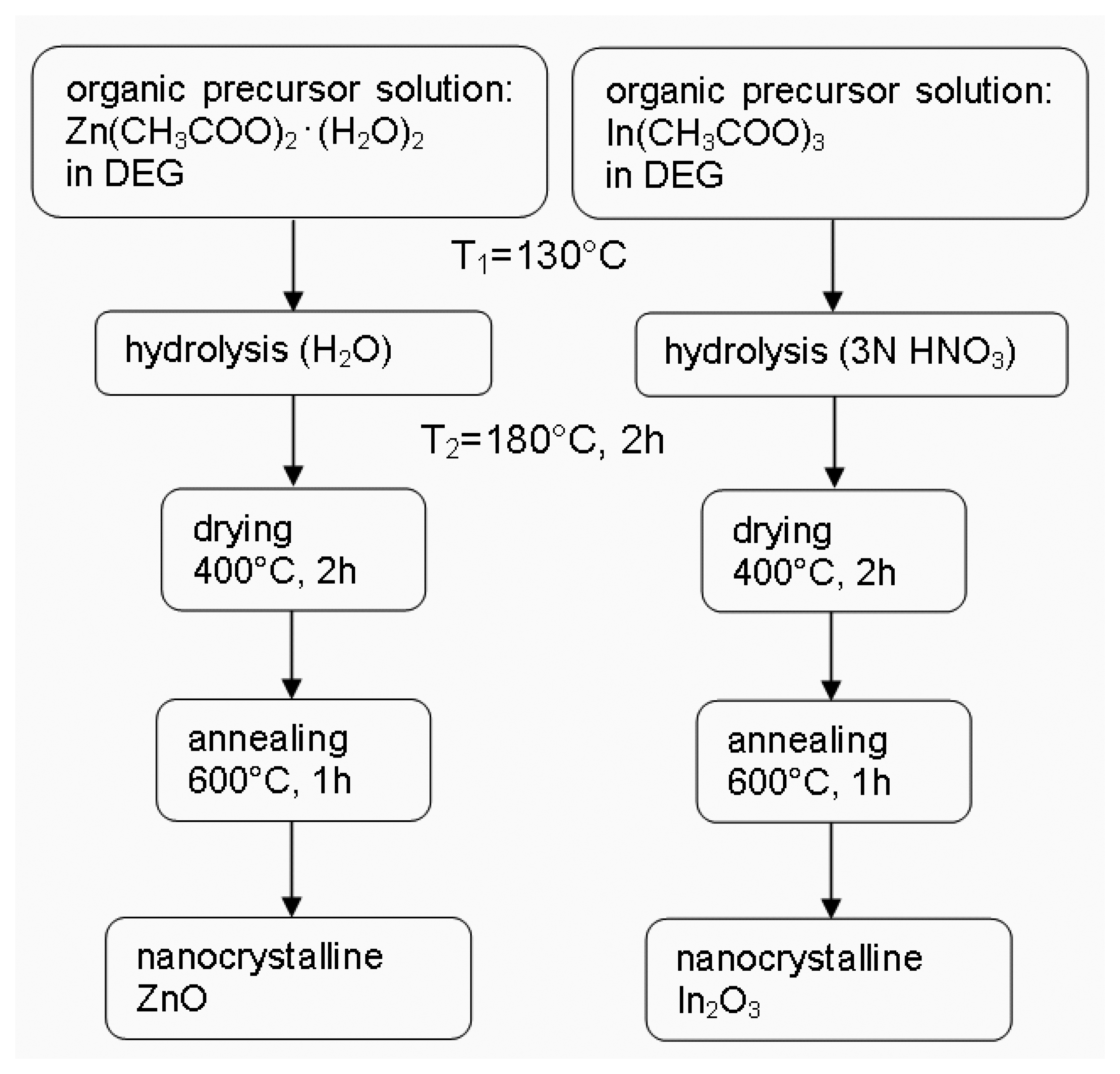
Material preparation
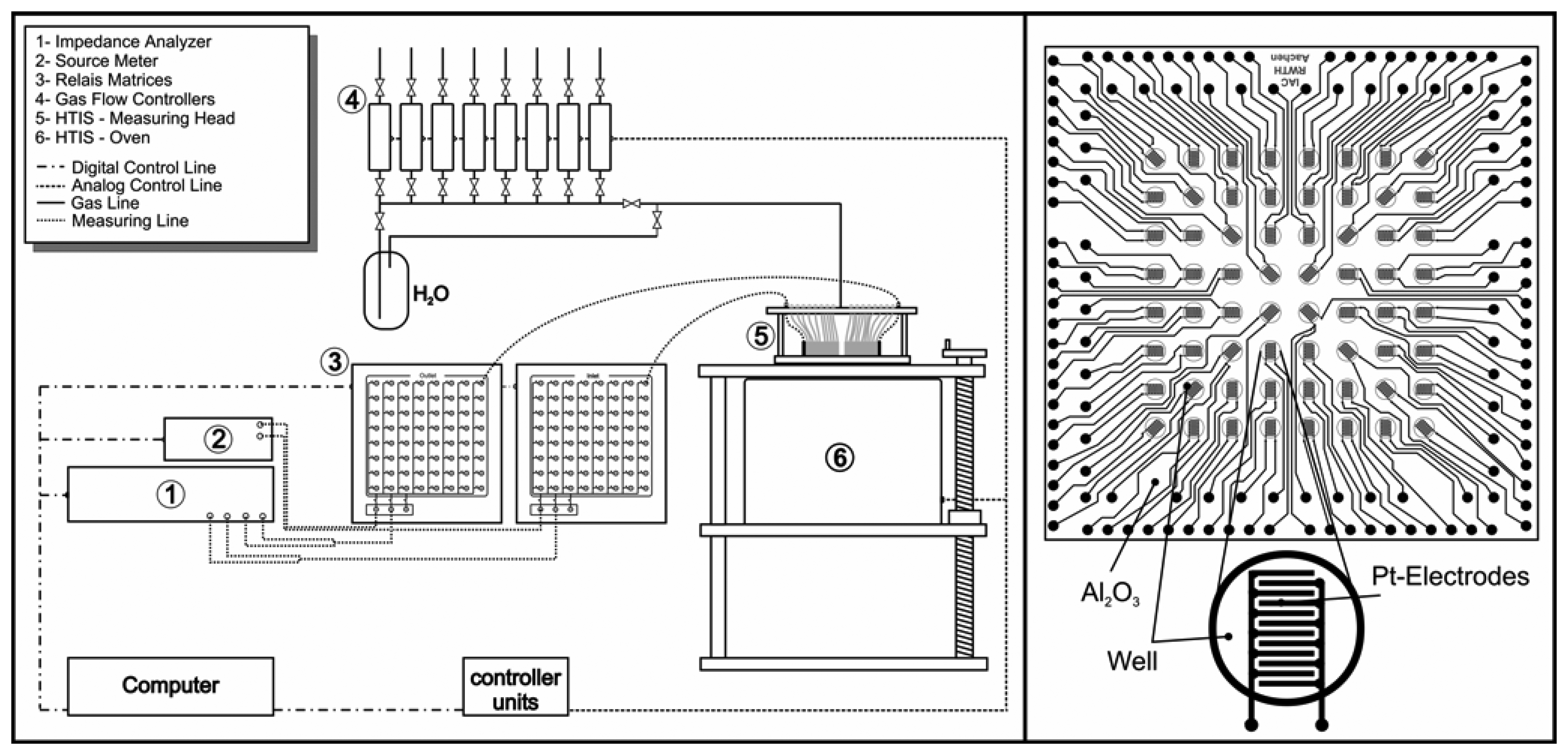
To prepare ZnO nanoparticles zinc acetate dihydrate (1.52 g, 6.9.10-3 mol) was dissolved in diethylene glycol (DEG) and heated up to 130°C until a clear solution was obtained (see Fig. 1, left). After adding water (2 ml) under vigorous stirring the resulting mixture was heated up to 180 °C for 2 hours, whereby the solution turned rapidly white turbid. To remove the organic solvent the resulting suspension was dried at 400 °C for 2 hours and then annealed at 600 °C for 1 hour. The resulting white powder of zinc oxide was confirmed by X-ray diffraction measurement (ZnO: ICSD 29272[20]) on films using a Guinier image-foil camera (G670, Huber GmbH) in transmission (Ge-monochromator, CuKα1, λ =1.5418 Å).
To prepare In2O3 nanoparticles indium acetate (0.67 g, 2.3.10-3 mol) was dissolved in diethylene glycol (DEG) and heated up to 130 °C until a clear solution was obtained (see Fig. 1, right). After adding nitric acid (2 ml, 3 N) under vigorous stirring the resulting mixture was heated up to 180 °C for 5 hours, whereby the solution turned gradually light brown turbid. After drying (400 °C, 2 h) and calcining at 500 °C (1 h) a yellow fine powder was obtained, which was identified as indium oxide by X-ray diffraction (ICSD 27999 [21]).
The powder morphology was examined by SEM analysis using a Zeiss DSM 982 Gemini. For that purpose, the samples were sputtered with carbon. The SEM pictures for both samples are shown in Figure 2. The mean particle diameter was 89 nm ± 19 nm for zinc oxide and 19 nm ± 3 nm for indium oxide.
For thick film deposition of zinc oxide on the interdigital electrodes, the powder material (407.8 mg, 5.01.10-3 mol) was first redispersed by grinding in a ball mill (30.9 g YTZ®-grinding media, Ø = 3 mm) with an aqueous polyethylene imine solution (1.0 wt.%) for 3 days. The resulting suspension was extracted and had a ZnO concentration of 0.835 mol/L. The suspension was deposited into wells formed by a Teflon mask (volume per well 214 μL) on top of the microelectrode substrates by a laboratory roboting system (Lissy, Zinsser Analytic GmbH), whereby each well had an O-ring for sealing against the substrate. After drying (60 °C, 1 day) and calcination (600 °C, 1 h) different aqueous preferably halide-free metal salt solutions with concentrations from 0.2 to 0.6 at.% were used for surface doping. The applied doping elements were Au (as HAuCl4·3H2O), Ce (as (NH4)2Ce(NO3)6), Ir (as Ir(C5H7O2)3), Pd (as Pd(NO3)2·2H2O), Pt (as Pt(NH3)4(NO3)2), Rh (as Rh(NO3)3·2H2O) and Ru (as Ru(NO)(O2C2H3)3). With respect to the deposited amount of zinc oxide per well (1.11 mg, 1.36.10-5 mol per well, Ø= 4 mm), a corresponding amount of solution was dispensed with the laboratory roboting system to achieve a surface doping of 0.1 or 0.5 at.%. The substrate was dried for 24 hours at 60 °C and after that annealed for 1 h at 600 °C in air to remove the organic residues. For preparation of the indium oxide thick films the powder material was ground in a mortar by adding a corresponding amount of salt solutions or water yielding in a surface doping of 0.5 at.%. The suspensions were transferred on the interdigital electrodes using an Eppendorf pipette. The substrate was dried for 24 hours at 60 °C and after that it was held for 1 h at 500 °C in air to remove the organic residues generating homogeneous films of indium oxide (0.3 mg, 1.06.10-6 mol per well).

Screening

Figure 3 shows the scheme of the HT-IS setup and the layout of the multielectrode array.
The multielectrode array consists of screen-printed platinum leads on an Al2O3 ceramic substrate (side length of 105 mm) forming 64 interdigital capacitors (IDCs). The platinum IDC has a structure width of 110 μm and each well has a diameter of 5 mm [10]. The array is capable for resistive as well as for capacitive measurements. In addition, the design allows efficient and automated pipetting robot assisted sample preparation and coating, respectively. Time-consuming process steps, like heating up or sample conditioning can be proceeded in parallel. Sample plates (coated arrays) are inserted in the measuring head. The leads to each IDC are electrically connected via Al2O3 covered platinum wires in the measuring head. Constant contact pressure is assured using spring loaded contact tips which connect the IDCs via high frequency capable relay matrices (multiplexers) to the measuring instruments. A set of gas flow controllers is used to compose the different test gases. In addition, the test gases can be humidified by bubbling the carrier gas through a water reservoir at room temperature. The test gases are led to a quartz glass bell covering all sample positions on a plate. For technical details see [12]. The whole system is controlled by a single self-made measuring and controlling software. As standardised screening sequence the materials are electrically characterised by complex impedance spectroscopy (Agilent 4192A: 10 - 107 Hz, amplitude 0.1 Vrms) in synthetic air (RH = 45% at 25 °C (air)) serving as reference, H2 25 ppm, CO 50 ppm, NO 5 ppm, NO2 5 ppm, propene 25 ppm at temperatures between 400 °C and 250 °C in 25° steps. Prior to each measurement, a preliminary gas flow was each 30 min. All test gas measurements are followed by a measurement in reference atmosphere to investigate the reversibility of the material response.

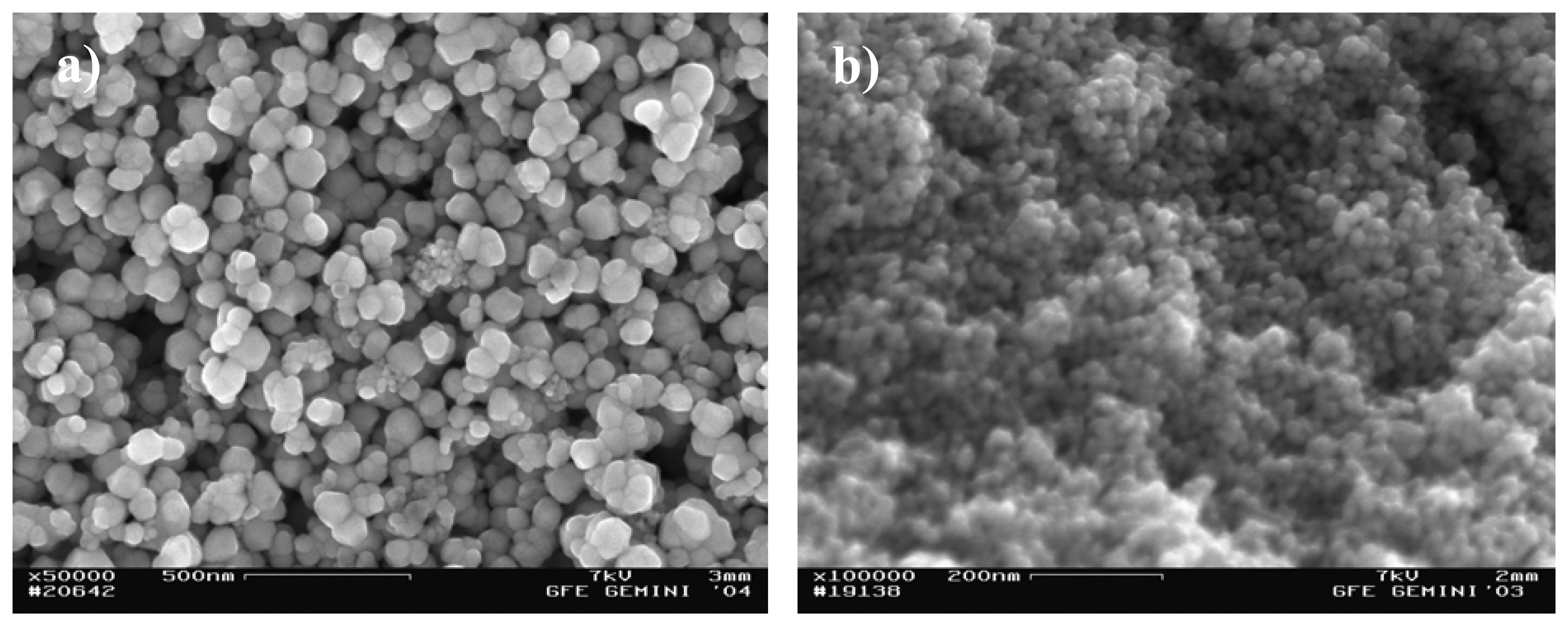
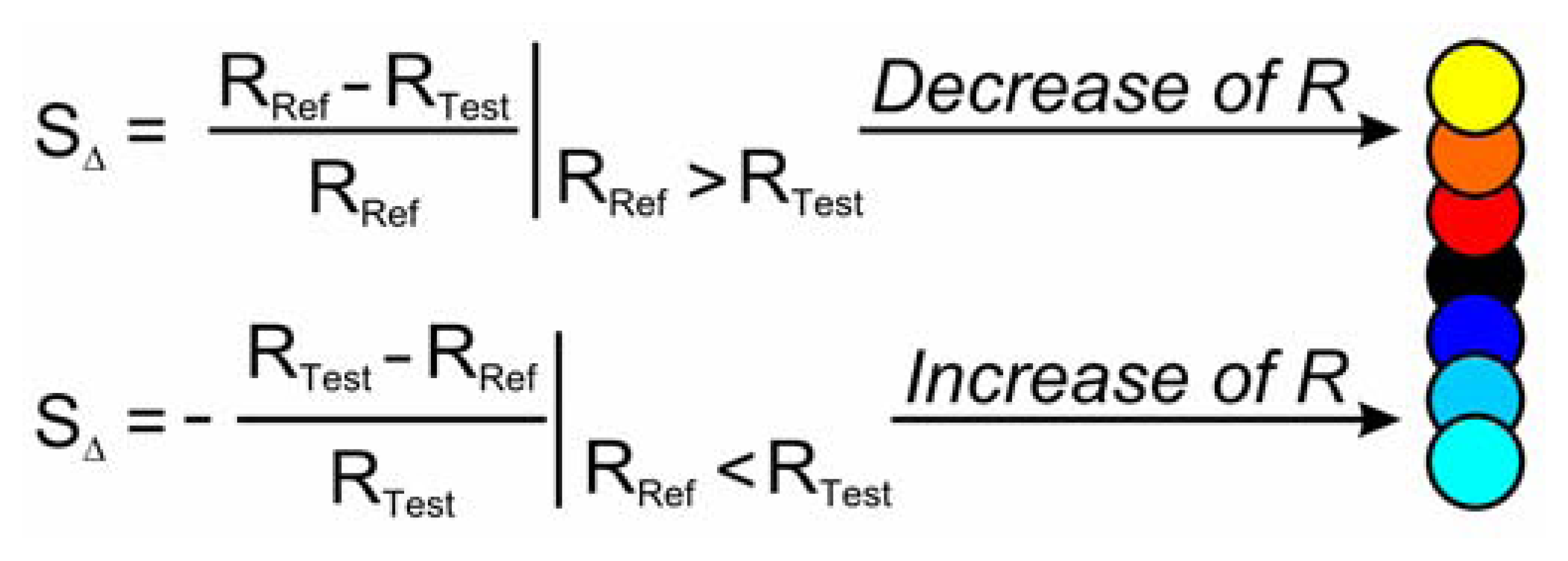
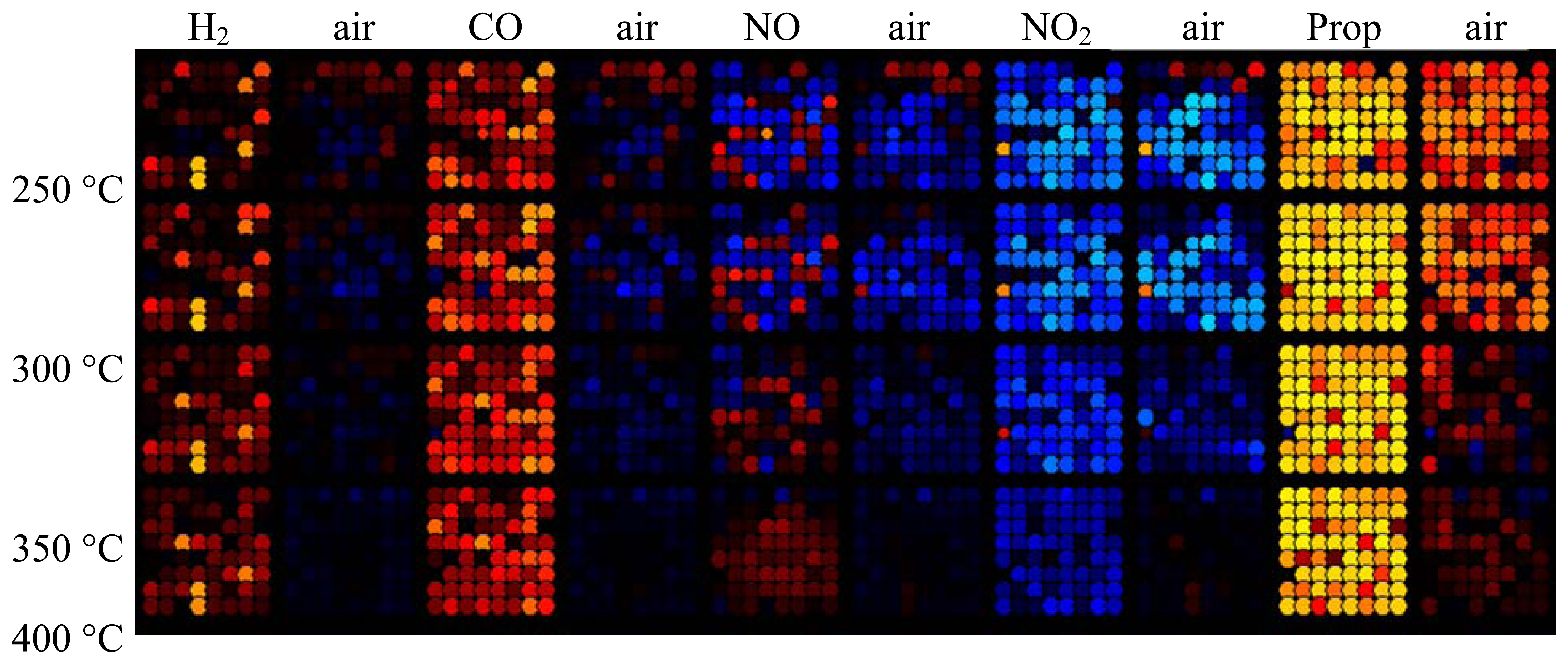
Results and discussions
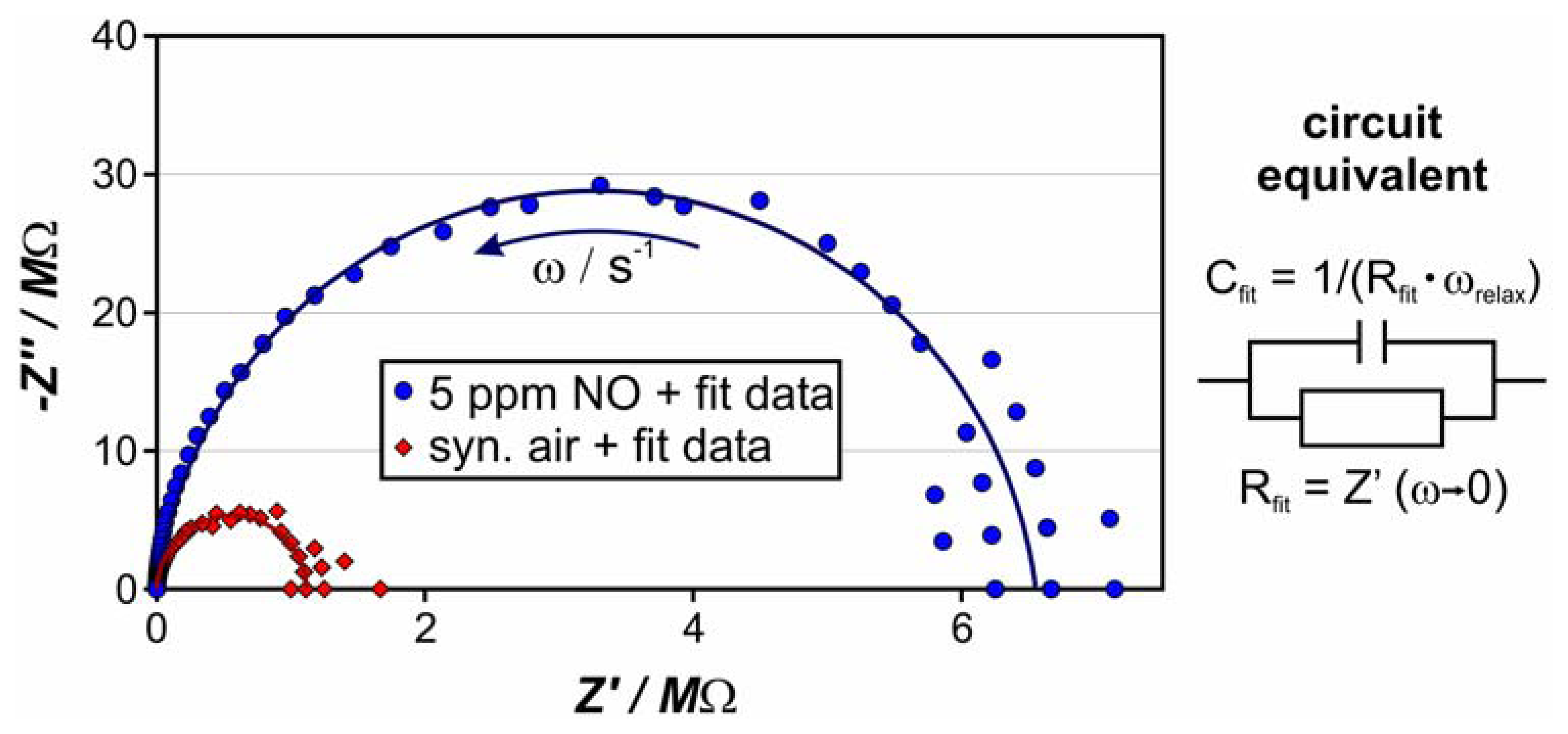
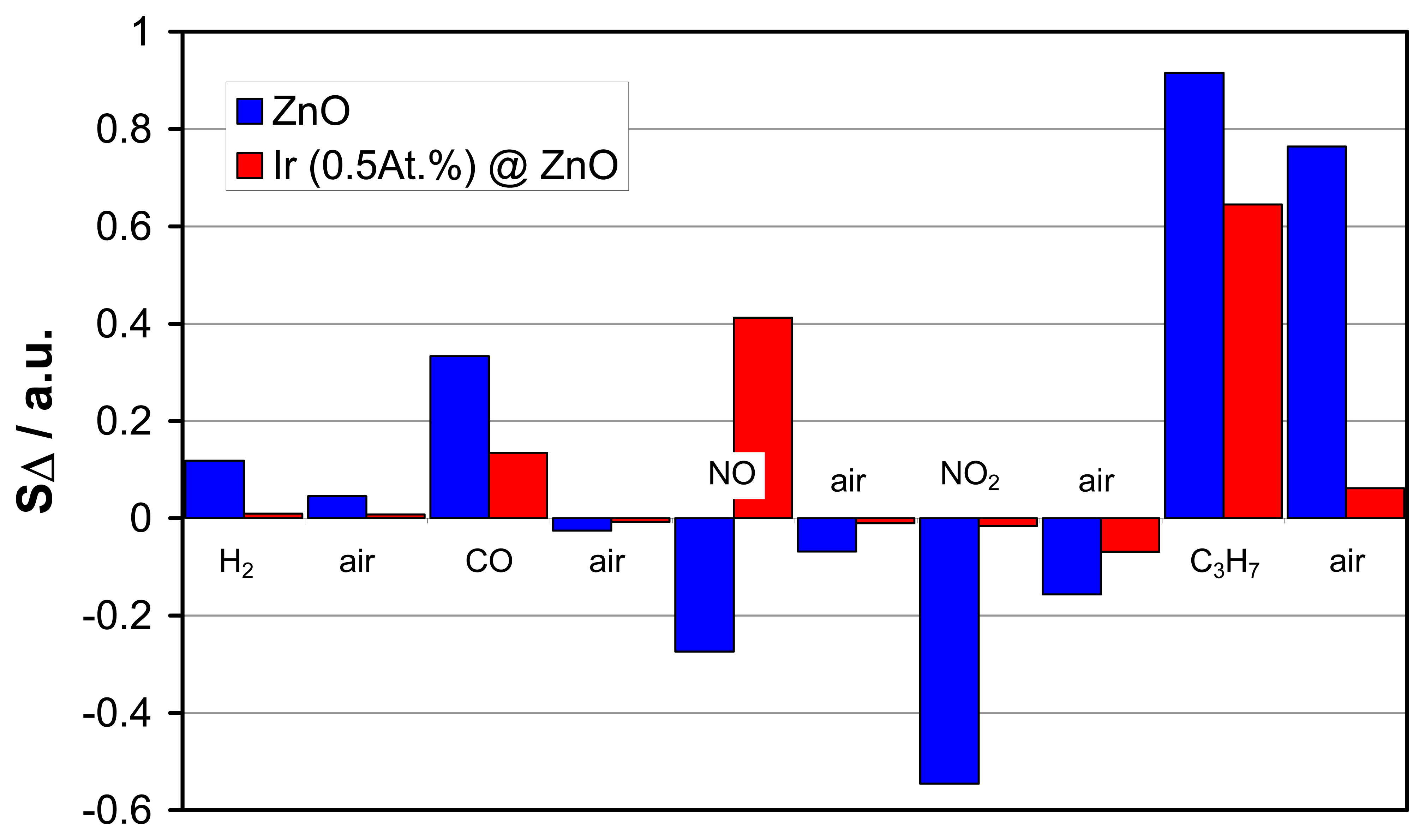
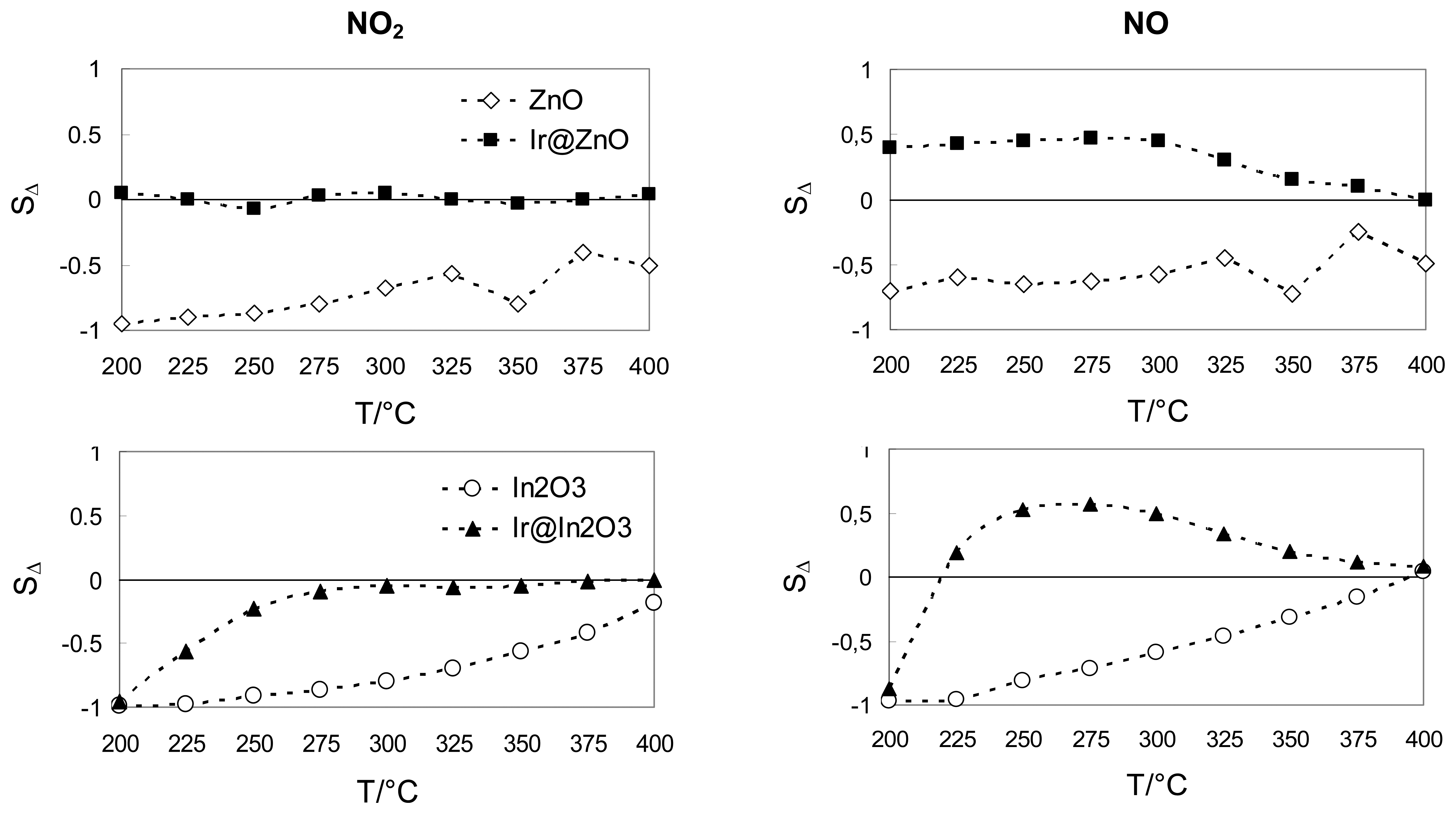
Figure 4 shows the plot of real part of the complex impedance versus the imaginary part (Argand plot) for Ir@ZnO in synthetic air and NO at 250 °C. The plots, which are representative for all other samples measured show one semicircle. Automated data fitting allows describing the impedance spectra with the impedance function of a circuit equivalent, consisting of a resistor and a capacitor in parallel. In this case Rfit is the extrapolated DC-resistance of the material, Cfit the capacitance and ϖ the angular frequency. The use data fitting allows to describe the complex impedance function for each material to one value for the resistance and the capacitance, respectively, leading to a data reduction which is vital for HTE. While the capacitance can be assigned to the geometric capacitance of the IDC, the resistance values under the respective measuring conditions are taken for the determination of the material sensitivity. Therefore, we describe the response of a material to a test gas by the relative sensitivity SΔ, which is defined as:
RTest is the resistance obtained from the fit under test gas, while RRef is the reference resistance value for a measurement under reference atmosphere. Values for SΔ range from 1 to -1. Decrease of resistance while applying a test gas gives values between 0 and 1, rise of resistance results correspondingly in values for SΔ between 0 and -1. Using SΔ instead of the commonly used sensitivity S including algebraic signs turned out to be beneficial for the data mining process in our high throughput workflow. Furthermore, it allows an immediate differentiation between oxidizing and reducing test gases, respectively. To display the sensitivity in a Trellis-plot the derived values of SΔ were translated into a colour code as illustrated in Figure 5. At the same time, the dot radius scales inversely with the measuring failure, resulting either from a broad scattering of the impedance values, or from an exceeding of the measurement range (e.g., impedance value above 20 M Ω).
For illustration of the evaluation process, the screening results of the surface doped zinc oxide plate at four different temperatures for the sequence of the five test gases is depicted in Figure 6. Accordingly, each 8×8 square matrix represents the sensitivities of the 64 material compositions at a distinct temperature and a distinct test gas condition.
Generally, all materials showed a pronounced sensitivity towards the reducing gases CO and propene and a minor change of resistance upon H2 exposure. For these test gases no major effect of the specific doping elements was observed. In contrast, a typical response towards the oxidising gases NO2 and NO (at lower temperatures) is an increase of the resistance displayed as negative values for SΔ and a blue-coloured dots, respectively. Despite of the measurement at 400 °C the resistance changes caused by NO and NO2 appear to be non-reversible on the timescale of the experiment.

Selected example

Figure 7 shows the relative sensitivity SΔ of undoped and iridium-doped zinc oxide, illustrating the effect of the surface dopand on the sensitivity. The undoped material is sensitive towards all tested gases, while NO2 and propene had the strongest effect on the materials resistance. It is obvious that the reaction with propene is not reversible on the timescale of the experiment. In contrast, the iridium-doped sample shows high sensitivity towards NO with, however, no cross sensitivity towards hydrogen and NO2. Sensitivities towards CO and propene appear to be reduced, while the reaction towards propene turns out to be reversible in the respective time scale. As a most striking feature the resistance change towards nitrogen monoxide is reversed when iridium is applied for surface doping. This indicates that the character of reaction of NO with the semiconductor surface is converted from an oxidizing to a reducing interaction, when iridium is present.
The temperature dependence of the sensitivity S towards NO and NO2 of both, doped and undoped ZnO, is depicted in Figure 8. In addition, the temperature dependence of SΔ of Ir-doped and undoped In2O3 is shown.
The Ir-doped ZnO sample shows no reaction towards NO2 over the whole temperature range. A significant signal upon exposure of NO can be observed from 200 to 325 °C. In contrast, the undoped base material responds with increasing SΔ at higher temperatures on both of the target analytes. This behaviour makes Ir-doped ZnO a promising NO2-tolerant NO sensing material in the temperature range from 200 to 375 °C. A similar influence on the sensitivity towards NO and NO2 was observed for indium oxide with iridium surface dopand. Undoped indium oxide responds on both of the target analytes below 400 °C. In case of Ir@In2O3, the sensitivity towards NO2 is almost fully suppressed in the temperature range from 275 to 400 °C and the sensing behaviour towards NO changed in the range from 225 to 400 °C. The mechanism which is responsible for the behaviour of the iridium-doped samples remains to be answered.

Conclusions

The HT-IS system presented is a valuable tool for rapid electrical characterisation of different semiconducting gas sensor materials. Using the substrate plates shown and the HT-IS system, allows screening a wide range of materials in a short time. For example 832 IS measurements with 91 single frequency measurements each at different temperatures and under different gas atmospheres, including preliminary gas run and cooling down can be performed in 124 h. Applying HT-IS in the finding of new gas-sensing materials focussing on highly selective materials, we identified a NO2-tolerant NO sensing material with reduced sensitivities towards the test gases H2, CO and propene. This iridium-doped ZnO nanoparticles represents a promising material for NO sensing in the temperature range from 200 to 375 °C. We observed analogous behaviour for iridium surface doping on nanoparticulate indium oxide. This material is suitable as NO2-tolerant NO sensor in the temperature range from 275 to 375 °C.

Acknowledgments

The authors thank the German federal ministry of education and research (BMBF FKZ03C0305) and the Robert Bosch GmbH for financial support and the Central Facility for Electron Microscopy at RWTH Aachen University for the SEM measurements. M. S. and T. J. K. gratefully acknowledge generous support by the Studienstiftung des Deutschen Volkes and Stiftung der Deutschen Wirtschaft, respectively.

References

  1. Seiyama, T.; Kato, A.; Fujiishi, K.; Nagatani, M. A new detector for gaseous components using semiconductive thin films. Anal. Chem. 1962, 34, 1502. [Google Scholar]
  2. Tagushi, N. Jpn. Patent 45-38200, 1962.
  3. Eranna, G.; Joshi, B.C.; Runthala, D.P.; Gupta, R.P. Oxide materials for developement of integrated gas sensors – A comprehensive review. Crit. Rev. Sol. State Mater. Sci. 2004, 29, 111. [Google Scholar]
  4. Maekawa, T.; Tamaki, J.; Miura, N.; Yamazoe, N. Sensing behaviour of CuO-loaded SnO2element for H2S detection. Chem. Lett. 1991, 575. [Google Scholar]
  5. Cabot, A.; Arbiol, J.; Morante, J.R.; Weimar, U.; Bârsan, N.; Göpel, W. Analysis of the noble metal catalytic additives introduced by impregnation of as obtained SnO2 sol-gel nanocrystals for gas sensors. Sens. Actuat. B 2000, 70, 87. [Google Scholar]
  6. Göpel, W.; Schierbaum, K.D. SnO2 Sensors: Current status and future prospects. Sens. Actuat. B 1995, 26, 1. [Google Scholar]
  7. Yamazoe, N.; Sakai, G.; Shimanoe, K. Oxide semiconductor gas sensors. Catal. Surv. Asia 2003, 7(1), 63. [Google Scholar]
  8. Franke, M.E.; Koplin, T.J.; Simon, U. Metal and metal oxide nanoparticles in chemiresistors: does the nanoscale matter? Small 2006, 2, 36. [Google Scholar]
  9. Jandeleit, B.; Schaefer, D.J.; Powers, T.S.; Turner, H.W.; Weinberg, W.H. Combinatorial materials science and catalysis. Angew. Chem. 1999, 111, 2648, In. Ed. 1999, 38, 2494. [Google Scholar]
  10. Hagemeyer, A.; Stasser, P.; Volpe, A.F., Jr. (Eds.) High-throughput screening in chemical catalysis; Wiley-VCH: Weinheim, 2004.
  11. Simon, U.; Sanders, D.; Jockel, J.; Heppel, C.; Brinz, T. Design strategies for multielectrode arrays applicable for high-throughput impedance spectroscopy on novel gas sensor materials. J. Comb. Chem. 2002, 4, 511. [Google Scholar]
  12. Franzen, A.; Sanders, D.; Jockel, J.; Scheidtmann, J.; Frenzer, G.; Maier, W.F.; Brinz, Th.; Simon, U. High-throughput method for the impedance spectroscopic characterization of resistive gas sensors. Angew. Chem. 2004, 116, 770, In. Ed. 2004, 43, 752. [Google Scholar]
  13. Simon, U.; Sanders, D.; Jockel, J.; Brinz, T. Setup for high-throughput impedance screening of gas-sensing materials. J. Comb. Chem. 2005, 7, 682. [Google Scholar]
  14. Figlarz, M.; Fiévet, F.; Lagier, J.P. Process for reducing metallic compounds using polyols, and metallic powders produced thereby. Europ. Pat. 0113281, 1982. [Google Scholar]
  15. Toneguzzo, Ph.; Viau, G.; Acher, O.; Guillet, F.; Bruneton, E.; Fievet-Vincent, F.; Fievet, F. CoNi and FeCoNi fine particles prepared by the polyol process: Physico-chemical characterization and dynamic magnetic properties. J. Mater. Sci. 2000, 35, 3767. [Google Scholar]
  16. Poul, L.; Ammar, S.; Jouini, N.; Fievet, F.; Villain, F. Synthesis of inorganic compounds (metal, oxide and hydroxide) in medium: A versatile route related to the sol-gel process. J. Sol-Gel Sci. Tech. 2003, 26, 261. [Google Scholar]
  17. Jézéquel, D.; Guenot, J.; Jouini, N.; Fiévet, F. Submicrometer zinc oxide particles: Elaboration in polyol medium and morphological characteristics. J. Mater. Res. 1995, 10, 77. [Google Scholar]
  18. Feldmann, C.; Jungk, H. Polyol-mediated preparation of nanoscale oxide particles. Angew. Chem. 2001, 113, 372, Int. Ed. 2001, 40, 359. [Google Scholar]
  19. Siemons, M.; Weirich, Th.; Mayer, J.; Simon, U. Preparation of nanosized perovskite-type oxides via polyol method. Z. Anorg. Allg. Chem. 2004, 630, 2083. [Google Scholar]
  20. Sabine, T.M.; Hogg, S. The wurtzite Z parameter for beryllium oxide and zinc oxide. Acta Crystallogr. B 1969, 25, 2254. [Google Scholar]
  21. Zachariasen, W. The crystal structure of the modification C of the sesquioxides of the rare earth metals, and of indium and thallium. Norsk Geologisk Tidsskrift 1927, 9, 310. [Google Scholar]
Figure 1. Reaction pathway for the polyol synthesis of ZnO- and In2O3-nanoparticles.
Sensors 06 00298f1
Figure 2. SEM-pictures of a) zinc oxide nanoparticles (Ø = 89 nm ± 19 nm) and b) indium oxide nanoparticles (Ø = 19 nm ± 3 nm).
Sensors 06 00298f2
Figure 3. Left: Scheme of the HT-IS setup. For reasons of clearness only two measuring lines are displayed. Right: Layout of the multielectrode array (adapted from [11,13]).
Sensors 06 00298f3
Figure 4. Argand plot and circuit equivalent of Ir@ZnO under synthetic air and NO. Ir@ZnO shows an increase of resistance compared to synthetic air, when NO is admixed (T=250 °C).
Sensors 06 00298f4
Figure 5. Calculation of the relative sensitivity and colour translation for the Trellis-plot.
Sensors 06 00298f5
Figure 6. Trellis-plot of the relative sensitivities of the sample plate - from top to bottom with increasing temperature (250 to 400 °C) and from left to right with the sequence of the test gases (H2, air, CO, air, NO, air, NO2, air, propene, air).
Sensors 06 00298f6
Figure 7. Relative sensitivity of undoped (blue) and iridium doped (red) zinc oxide (T = 300 °C).
Sensors 06 00298f7
Figure 8. Temperature dependence (200-400 °C, data were taken every 25°) of SΔ for Ir-doped and undoped zinc and indium oxide towards NO and NO2.
Sensors 06 00298f8

