Abstract
We present a 1024 × 512, 1000 fps, high-dynamic-range global shutter CMOS image sensor. The pixel is based on a voltage domain global shutter architecture, featuring a pitch of 24 μm × 24 μm. Both high-gain and low-gain signals can be captured within a single frame. The combined dynamic range is 95 dB, and the full well capacity is 620 ke-. In this paper, we analyze the pixel noise performance as well as the non-linearity and image lag that arise from parasitic capacitance in the pixel. The ramp generator is based on a 12-bit full thermometer code current-steering DAC with high driving capability. We discuss the design considerations for the ramp generator, particularly addressing the phenomenon of non-linear response. Finally, the comparator design and the column readout noise are analyzed.
1. Introduction
We present a CMOS image sensor (CIS) with a 24 μm × 24 μm global shutter pixel, suitable for scientific, industrial, and medical applications [1,2]. There are three types of global shutter (GS) pixel: a charge domain GS pixel, a voltage domain GS pixel and a pixel with pixel-parallel ADC [3,4]. The voltage domain GS pixel is particularly advantageous for large pixel designs or processes involving high-density metal capacitors [5], as it offers a larger full well capacity due to the independence of the voltage storage node from the pinning voltage. The 8T and 10T architectures represent two classical configurations for voltage domain GS pixels [6,7]. The correlated double sampling (CDS) operation is performed within the readout circuit. This paper analyzes both the noise performance of the voltage domain GS pixel and the requirements for the readout circuit. Additionally, we extend the dynamic range by employing four storage capacitors within each pixel, enabling simultaneous capture of high-gain and low-gain signals in a single frame.
Single-slope ADC (SS-ADC) is widely used in CISs [8]. In a CIS, the SS-ADC mainly consists of a ramp generator, a comparator and a counter. There are several architectures for the ramp design, including column level, chip level, and multi-column shared ramp generator. With a chip-level ramp generator, the SS-ADC can achieve better uniformity compared to SAR ADCs and cyclic ADCs [9]. The column level and multi-column shared ramps are typically based on current integration architecture, which suffers from random walk noise and kick-back noise [10,11]. For the design of large array CISs, the length of the ramp bus may extend several centimeters from one side of the array to the other. A distributed multiple ramp signal generator based on current integration architecture demonstrates good uniformity [12,13]. To achieve low-noise performance in such designs, a current-steering (CS) DAC can be employed as the ramp generator [14]. The heavy capacitive load presented by the column array effectively acts as a low-pass filter for the CS-DAC ramp, thus, its noise contribution can be considered negligible when compared to that from pixels and comparators. In conventional CS-DACs, current source arrays are generally organized using a segmented architecture that consists of a binary-coded least significant bit (LSB) array and a thermometer-coded most significant bit (MSB) array. However, in CIS applications where DAC functions as a ramp generator, sequential control over each current source within the array is necessary. This paper presents an innovative 12-bit full thermometer code current-steering DAC utilizing shift registers for digital control.
The comparator is a crucial component in SS-ADCs. Both dynamic comparators [14,15] and static comparators [4,11] can be implemented in a CIS. The comparator has two inputs: one is the output from the pixel or the programmable gain amplifier (PGA), while the other is the ramp signal. In the case of a static comparator, its first stage consists of a transconductance amplifier with ramp response, which can be modeled as a low-pass system [16]. This paper presents a comparator that incorporates a current compensation block. Additionally, we analyze the noise from the pixel source follower, column current source, column ramp buffer and the comparator itself.
Finally, the performance characteristics of this CIS are presented. It is fabricated in a standard 110-nm backside illumination (BSI) CIS process, and the array format is 1024 × 512. The frame rate achieves 1000 fps in single gain mode and 500 fps in dual gain mode. The combined dynamic range is measured at 95 dB.
2. CMOS Image Sensor Design
2.1. Global Shutter Pixel Design
2.1.1. Basic Voltage Domain Global Shutter Pixel
In this design, the voltage domain GS pixel is used for a specific application. Metal capacitors can be employed for the storage node while ensuring a large full well capacity (FWC). The 8T and 10T pixels represent two classical configurations of voltage domain GS pixels. The CDS operation is performed within the column readout circuit.
Figure 1 and Figure 2 show the basic 8T pixel and 10T pixel, respectively. The difference is the signal storage chain within each pixel. In the case of the 8T pixel, both the reset signal and light signal are read out through the same source follower (SF), which leads to charge-sharing between CS and CR. The input-referred thermal noise for both 8T and 10T pixels after CDS can be expressed as:
where k is the Boltzmann constant, T is the absolute temperature, γ is the noise excess factor, Vn-col is the thermal noise at the pixel output node originating from the SF2 to ADC chain, and G1 and G2 are the gains of SF1 and SF2, respectively. Additionally, CR and CS are the sampling capacitors in the pixel, both of which are equivalent to CGS in this discussion. The factor 2 represents CDS operation. The factor 0.5 in the second term represents the charge-sharing phenomenon within an 8T pixel. From Equations (1) and (2), we know that transconductance and capacitance are important for the voltage domain GS pixel design. Figure 3 shows the comparison results of thermal noise. Under the same column readout conditions, the noise performance of the 10T pixel is always better, especially for GS pixels with larger CGS. In other words, the 10T pixel relaxes the requirements on the column readout.
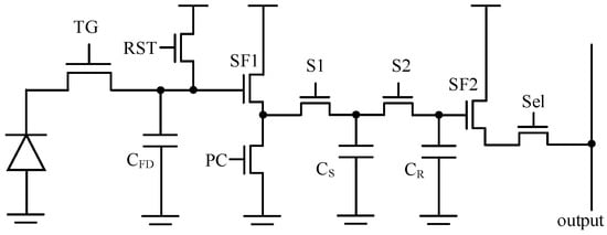
Figure 1.
8T global shutter pixel.
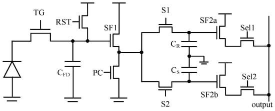
Figure 2.
10T global shutter pixel.
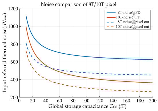
Figure 3.
Input-referred noise comparison of 8T/10T pixel at T = 300 K, gmSF/gmPC = 0.4, γ = 2/3, G1 = G2 = 0.85, Vn-col = 150 uVrms.
2.1.2. High-Dynamic-Range 10T Pixel Design
Figure 4 shows the proposed high-dynamic-range global shutter pixel. There are two separate channels, enabling the capture of high conversion gain (HCG) and low conversion gain (LCG) signals within a single frame. SLR + CLR, SLS + CLS, SHR + CHR, and SHS + CHS correspond to the LCG reset signal VLR, LCG light signal VLS, HCG reset signal VHR, and HCG light signal VHS, respectively. In this design, CLR = CLS = CHR = CHS = 120 fF, CFD = 4 fF, CLG = 60 fF, gmSF1/id = 15, and gmPC/id = 6. The estimated input-referred thermal noise at the FD node (Vn-col = 0) is approximately 275 μVrms.
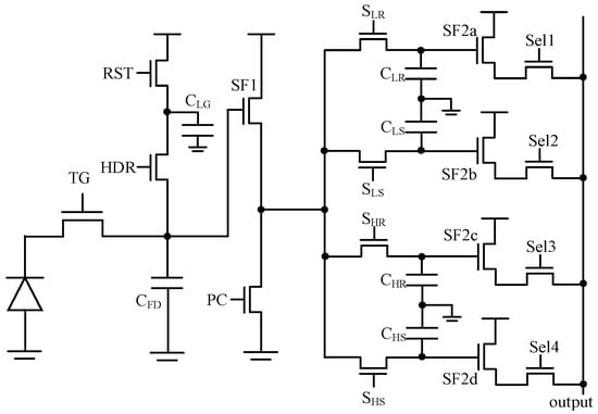
Figure 4.
10T + HDR global shutter pixel. (TG, Transfer Gate; RST, reset transistor; HDR, high dynamic range switch; Sel, row select transistor).
The parasitic capacitances in the proposed GS pixel affect both linearity and image lag performance. Figure 5 shows the timing diagram for the global charge transfer phase. Initially, VLR is stored on CLR, and the voltage signal is locked at time t1. This indicates that CLR should be isolated from CHR, CHS and CLS when SHR, SHS and SLS are set to high. For example, assuming that there is parasitic capacitance CLR-HS between CLR and CHS, the variation of VLR after the completion of VLS sampling can be expressed as:
where frameN.t3 and frameN.t1 mean the voltage signal at times t3 and t1 within frame N, respectively.
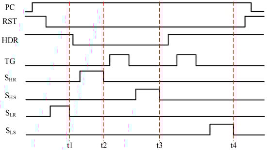
Figure 5.
Timing diagram for the global charge transfer phase for a 10T + HDR global shutter pixel.
- (1)
- Non-linearity: When the in-pixel storage capacitors are reset for each frame, parasitic capacitance can significantly impact the linearity of the LCG signal, e.g., CLR-HS = 0.5 fF, CLR = 100 fF, VHS variation from t1 to t3 is 1 V, and the result of VLR variation calculated using Equation (3) is 5 mV. Given that the ratio of HCG to LCG is 15, this will affect the linearity of LCG’s response within the range of 0% to 15%. In contrast, within the range of 15% to 100% of LCG, HCG remains saturated, and a fixed offset will be observed in LCG’s response. Note that the parasitic capacitances CHR-HS and CLR-LS between the capacitors belonging to the same gain channel have an influence on the light response across the entire range.
- (2)
- Image Lag: In the absence of a reset operation for the in-pixel storage capacitors following column readout, Equation (3) can be rewritten as:
The signal from the previous frame can influence the current frame in the presence of parasitic capacitance, e.g., CLR-HS = 0.1 fF, CLR = 100 fF, and assuming that the current frame is entirely dark while the HCG light signal from the previous frame is 1.2 V, the VLR variation calculated using Equation (4) is 1.2 mV.
For the same reason, CHR should be isolated from both CHS and CLS, and CHS should be isolated from CLS, as illustrated in the timing diagrams presented in Figure 5. Additionally, the parasitic capacitance between the source node of SF1 and the four storage capacitors also affects the signal accuracy. In conclusion, it is essential to minimize the parasitic capacitances among all five nodes, including the source node of SF1 and the four storage capacitors.
Figure 6 shows an example of the pixel layout. The pixel pitch is 24 μm and the fill factor is 70%. The four storage capacitors are utilized by two MOS capacitors and two MIM capacitors. The two MOS capacitors are isolated from each other by the contacts located between metal 1 and the active region. These contacts are connected to the ground and, thus, shield the electric field lines. In this design, the parasitic capacitances among the five nodes remain below 0.01 fF.
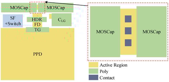
Figure 6.
Pixel layout example with isolated MOS capacitors.
2.2. Readout Circuits Design
2.2.1. Readout Architecture
The output swing of the proposed pixel is approximately 1.3 V, utilizing a design with a 1.4 V pinning voltage (Vpin) and 0.85~0.88 SF gain. As previously mentioned, the input-referred thermal noise of the GS pixel before the SF2 stage is 275 μVrms, which means the noise performance of the sensor is limited by the pixel if the ADC resolution ≥ 12 bits. The quantizing noise of a 12-bit ADC is 92 μVrms within a range of 1.3 V, and the total noise for such an ADC generally remains below 1 LSB. In this design, GS pixel + column ADC architecture is used.
The array format of this sensor is 1024 × 512, with a maximum frame rate of 1000 fps in single gain mode. The effective row time for one column is 1.9 μs. Figure 7 shows the architecture of the proposed CIS. Due to the 24 μm column width and the limitation of the 110 nm CMOS process, there are four SS-ADCs for each pixel column. The clock frequency for the counter operates at 500 MHz. To match the pixel output swing, the ADC input range is slightly higher than 1.3 V at × 1 gain.
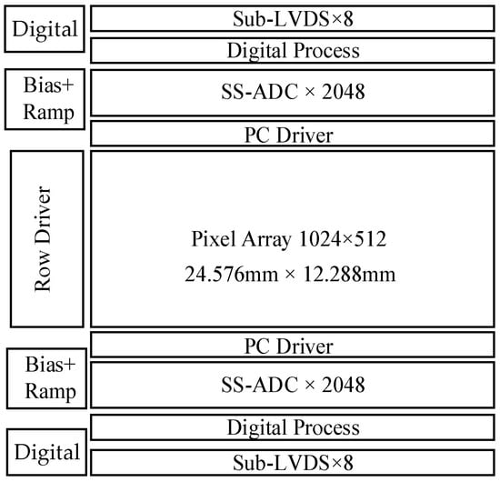
Figure 7.
Architecture of the proposed CMOS image sensor.
2.2.2. PC Driver Design
In the GS pixel, the pre-charge (PC) transistor is utilized for voltage sampling. The charging current is determined by both the capacitance of the storage node and the requirements for settling time. Typically, the current IPC ranges from several hundred nA to 1 μA. In this design, the current IPC is set at 1 μA, and the duration of the global charge transfer phase is 10 μs. Consequently, the total current across the entire pixel array during this phase approximates 524 mA. Therefore, it is important to consider the topology of the power supply for the voltage domain GS pixel array.
Figure 8 shows the PC driver circuit, which is based on the current mirror circuit. The nMOS transistor DPC must be identical to the type of PC transistor used in the pixel, and thus the current IPC in a pixel can be exactly controlled. To ensure that the settling time of the column bus for the PC bias remains under 1 μs, the current of the PC driver per column IDPC is set to 4 × IPC in this design.
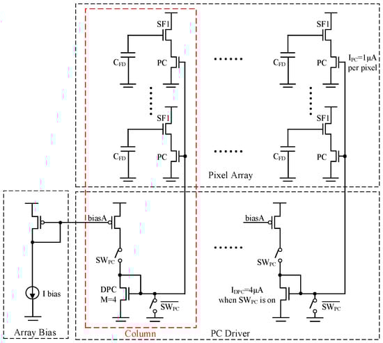
Figure 8.
Architecture of the PC driver circuit.
2.2.3. Ramp Generator Architecture
The input range of the SS-ADC is directly determined by the ramp reference. There are several architectures for the ramp design, including column level, chip level and a multi-column shared ramp generator. A chip-level ramp generator is employed to achieve better uniformity.
In this sensor, the length of the ramp bus is approximately 2.46 cm. The row time of the column ADC is 7.6 μs at 12-bit resolution operation. High driving capability is necessary for the ramp generator, which is utilized by a current steering DAC. Figure 9 shows the architecture of the ramp generator and column load. There is a pMOS SF buffer for each column between the ramp bus and the comparator. The column ramp buffer consumes 2 μA current. The noise originating from the column ramp buffer can be effectively filtered by the comparator, and it will be discussed in more detail later.
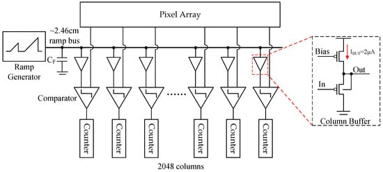
Figure 9.
Architecture of the ramp generator and column load.
Different from a classical current steering DAC application, the DAC output in a CMOS image sensor is certainly a ramp signal. It means that the control sequence for each unit cell operates sequentially. So a full thermometer code current-steering DAC is employed in this design, which effectively eliminates output glitches. Figure 10 shows the architecture of the proposed ramp generator. It is basically a current steering cell array with 100 columns × 50 rows. The total array consists of 5000 cells and supports digital double sampling (DDS) operation at a resolution of 12-bit. A maximum of 904 (5000 − 4096) cells can be used for the ramp adjustment. To generate the thermometer code, three shift register blocks are employed. The column control signal φcol is derived from two identical shift registers, SRT1 and SRT2, by utilizing an inverted input clock operating at 500 MHz. The row control signal φrow is generated from register SRL with a 5-MHz input clock. The unit current steering cell (UCSC) consists of a current steering circuit and a logic cell. Figure 11 shows the logic cell in a UCSC. For odd rows, current flows to out1 when φcol = high, φrowN = high, and φrow(N+1) = low. For even rows, the current flows to out1 when φcol = low, φrowN = high, and φrow(N+1) = low. When φrow(N+1) = high, the current of the entire row N flows to out1.
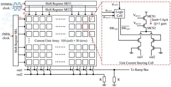
Figure 10.
Architecture of the ramp generator.
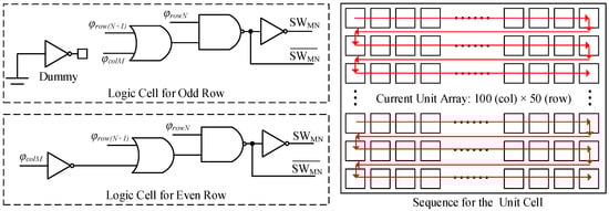
Figure 11.
Logic in a unit current steering cell.
The linearity of a CIS with pinned photodiode is usually limited by the pixel [17]. The non-linearity of a CIS is typically 1% ± 0.5%, which is highly dependent on the design of the FD node and the source follower in the pixel. The measured non-linearity of the entire sensor is 1.09% at high gain and 0.78% at low gain, respectively. The geometry of the MCS1 in the UCSC and the overdrive voltage are optimized for the purpose of mismatch improvement. In this sensor, the geometry of MCS1 is W/L = 0.5 μm/1 μm, and the default current of the UCSC is 1.6 μA, which can be adjusted to achieve different analog gains. The simulated mismatches of the current for one UCSC and for an array of 4096 USCSs are 1.38% (1σ) and 0.0214% (1σ), respectively. In this sensor, the load resistor R is 200 Ω, and the voltage swing of 4096 steps is 1.31 V at × 1 gain. The area of the ramp generator is 570 μm (H) × 320 μm (V).
2.2.4. Ramp Generator Analysis
The simplified schematic diagram of the proposed ramp is presented in Figure 12. The resistance R should match the requirements for the driving capability. The capacitance CF discussed in this chapter consists of both the parasitic capacitance and the load of the ramp. The effective resistance of the unit current source exceeds one million Ω at least, while the load resistance R is generally several hundred Ω. Consequently, the finite resistance of the current source is neglected in the following discussion.
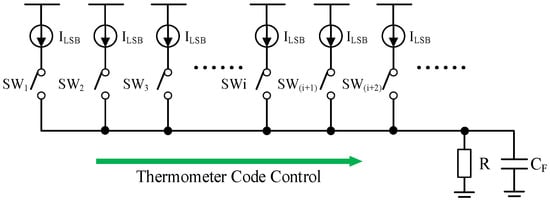
Figure 12.
Simplified schematic diagram of the ramp.
The step response of the 1 st LSB current source in time domain is given by:
where τ = RCF is the time constant. The step response of the i-th LSB current source with a time shift (i − 1)T0 can be expressed as:
where T0 is the time for one step. As shown in Figure 13, the ideal response of the ramp can be considered as the summation of multiple unit step responses with different time shifts. This relationship can be expressed as:
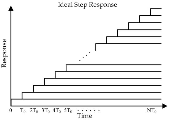
Figure 13.
Summation of multiple unit step responses.
Figure 14 shows an example of the ramp response curves with different CF values, where T0 = 1 ns and R = 200 Ω. Under the condition that τ << T0, e.g., τ = 0.2 ns (CF = 1 pF, R = 200 Ω), distinct steps can be observed. Under the condition that τ > T0, the step disappears, and a smooth curve is obtained. A non-linear response phenomenon is observed at the very beginning of the curve. If the time is long enough, e.g., several tens of nanoseconds, the slopes of the curves with different τ will converge to the same value but maintain a fixed offset from one another. In this design, the parasitic capacitance of the ramp output node is approximately 15 pF, which means that the ramp output can be directly connected to the column array without a real capacitor between the two blocks.
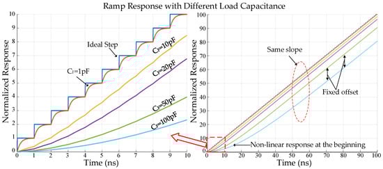
Figure 14.
Ramp response with different CF (R = 200 Ω, T0 = 1 ns).
Analyzing the response between t = (N − 1)T0 and t = NT0, we obtain:
The output increment between t = (N − 1)T0 and t = NT0 is given by:
The gain GN is determined by the settling time of the ramp, with a range from 0 to 1. Rstep represents the ramp response of a unit step under the condition that N >> 1. Figure 15a shows the relationship between GN and N. Assuming that the acceptable gain error is <1%:
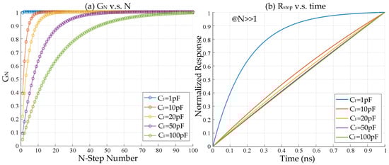
Figure 15.
(a) Gain vs. N; (b) ramp response of unit step (R = 200 Ω, T0 = 1 ns).
Under the condition that R = 200 Ω and T0 = 1 ns, the minimum number of steps Nmin to achieve the target gain 0.99 when CF = 1 pF, CF = 10 pF, CF = 20 pF, CF = 50 pF, and CF = 100 pF are 1, 10, 19, 47, and 93, respectively. Figure 15b shows the relationship between Rstep and time. The response curve approximates a straight line when τ = RCF is sufficiently large. The maximum difference between Rstep and the ideal ramp when CF = 15 pF is 0.04 LSB, which is given by:
The 0.04 LSB difference can be neglected even without an additional capacitive load. In this design, the output of the ramp is connected to the column array, which can be considered as an RC network. The simulated time delay for the ramp response from the first column to the 2048th column is 22 ns. The influence of the delay could be easily compensated through DDS operation and 904 redundant UCSCs.
According to Equations (11)–(14), the load resistor R and the clock frequency are important for implementing current-steering ramps in a CIS. For CISs operating at relatively low frame rates, the resolution of the ramp could be increased by using a real capacitor between the ramp and column array, e.g., a 14-bit ramp can be achieved from a 12-bit current-steering ramp when coupled with a suitable filtering capacitor. For CISs designed for high frame rates, utilizing a smaller resistance R is advantageous as it reduces the time constant, e.g., R = 100 Ω. Due to the high driving capability of the ramp and the isolation provided by the column ramp buffer, this architecture could be used in a stitched CIS, and the parasitic RC of the ramp bus must be carefully controlled.
2.2.5. Comparator Design
In this CIS, the output of the pixel is directly connected to the input of the comparator without a sample and hold circuit between them. Figure 16 shows the architecture of the comparator. It is based on a two-stage static comparator with a current compensation block. The first stage of the comparator consists of a transconductance amplifier (M1-M5), auto-zero switches AZ1 and capacitors CAZ1, a decoupling capacitor CB, and a refresh switch RF. The second stage consists of M6-M11, auto-zero switch AZ2 and capacitor CAZ2. In this design, CAZ1 = 400 fF, CAZ2 = 600 fF, CB = 600 fF, and dummy switches are employed.
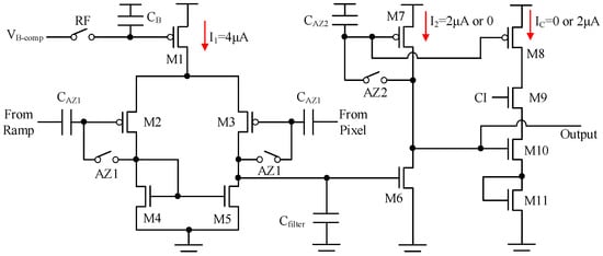
Figure 16.
Architecture of the comparator with current compensation.
Figure 17 shows the timing diagram for the column readout. At the beginning of each cycle, the comparator is reset by the auto-zero switches AZ1 and AZ2 to improve offset and mismatch. Additionally, the decoupling capacitor CB is reset to optimize the row-wise noise. The effective input capacitance of the comparator when AZ1 is on is 400 fF (CAZ1), while it drops to 20 fF when AZ1 is off. Both AZ1 and AZ2 turn on after the full-range ramp resets to VR0. Due to the voltage domain GS pixel architecture, light signals can be read out first, which corresponds to the small ramp. Between the two ramps, the reset signal is selected for output transmission. It should be noted that the pixel timing and the operational points must be optimized in order to prevent unintended activation of switch AZ1. CI is the timing control for current compensation. When the counter flag is high, the summation of I2 and IC remains nearly constant, thereby improving IR-drop performance across the entire array.
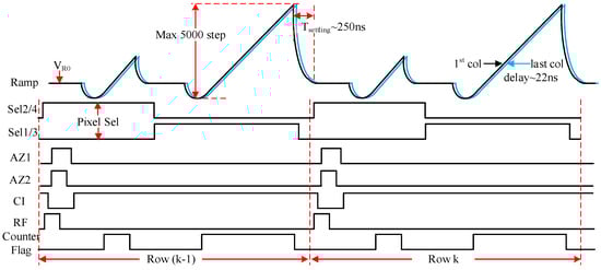
Figure 17.
Timing diagram for the column readout.
The noise performance can be improved as follows:
- (1)
- To improve low-frequency noise and avoid column flicker noise originating from the input transistors of the column readout, pMOS input transistors M2 and M3 are employed. The area of the input transistor is 10 μm2 for the purpose of low-frequency noise improvement.
- (2)
- The first stage of the comparator is actually an operational transconductance amplifier. The transfer function for a step ramp t × u (t) is 1/s2. The response in the time domain can be written as [8]:
Assuming the threshold voltage for the second stage transition is Vth-2nd and the gain of the second stage is sufficiently large. The time average crossing time Ti can be expressed as:
For the first stage, the noise bandwidth of the input-referred noise is similar to the usual one-pole system, and the effective noise bandwidth can be written as [16]:
By substituting Equation (18) into (19), we obtain:
Actually, the noise originated from pixel SF2, the column current source and the transconductance amplifier can be effectively filtered within the time window Ti by the sinc-type filter. Thus, the thermal noise at the pixel output node before DDS can be estimated as:
where γ is the noise excess factor, gmSF2, gmCS, gm1st-L, gmbuf-in and gmbuf-L are the transconductance of pixel SF2, column current source, comparator load transistors of the first stage (M4/M5) and column ramp buffer transistors, respectively. The CDS/DDS operation will result in a doubling of the thermal noise power. An increased value of gm1st is beneficial for reducing noise from the comparator, however, it worsens the noise from SF2 and the column ramp buffer due to the increase in NBW. Usually, gmSF2 is sufficiently large for fast settling. For low-noise applications, gmbuf-in should be large enough, and this requirement may lead to higher power consumption.
Figure 18 shows the calculation results derived from Equations (18), (20) and (21). The parameters used in the calculations are as follows: Kramp = 0.32 V/μs at ×1 gain, gm1st = gmbuf-in = 30 μS, gmSF2 = 120 μS, gmCS = 50 μS, gm1st-L = 15 μS, gmbuf-L = 12 μS, R1st = 14 MΩ, G2 = 0.85, Vth-2nd = 0.4 V (low-VT nMOS), and Cfilter = 150 fF (including parasitic capacitance). The noise bandwidth decreases with the increase of the ramp slope, Kramp. The calculated thermal noise at ×1 gain (ILSB = 1.6 μA) and ×4 gain (ILSB = 0.4 μA) after DDS are 128 μVrms and 90 μVrms, respectively.
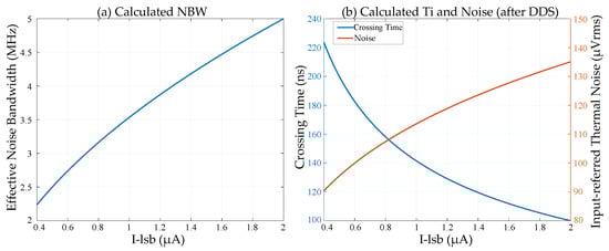
Figure 18.
(a) Calculated NBW; (b) calculated Ti and noise at 300 K (thermal noise after DDS).
Figure 19 shows the circuit simulation results of the crossing time and the input-referred noise after DDS, which includes thermal noise and low-frequency noise originating from the comparator, pixel SF2, column current source and column ramp buffer. The interval TDDS between the two crossing points of DDS signals is 1.2 μs under dark conditions, which affects the low-frequency noise performance according to the CDS/DDS transfer function 2 × cos(2πfTDDS). The simulated input-referred noise at ×1 gain (ILSB = 1.6 μA) and ×4 gain (ILSB = 0.4 μA) after DDS are 145 μVrms and 103 μVrms, respectively.
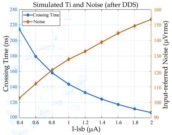
Figure 19.
Simulation results: Ti and noise at 300 K (including thermal and 1/f noise).
3. Results
Our sensor was fabricated with a standard 110 nm backside illumination (BSI) CIS process. The pixel pitch was 24 μm, and the array format is 1024 × 512; Figure 20 shows a photograph of the sensor. Both HCG and LCG images can be captured within a single frame. Figure 21 shows the photo response curves captured in dual gain mode. In this sensor, the FWC of the HCG signal was limited by the FD node, with a maximum output of 4096 DN. The FWC of the LCG signal was limited by the photodiode, resulting in a maximum output that is slightly lower than 4096 DN. The sensitivity ratio between HCG and LCG was approximately 16:1. The pixel process was optimized, and the FWC for LCG was 620 ke-. The noise in HCG mode was 10e-rms at ×1 ADC gain (ILSB = 1.6 μA), which corresponds to 320μVrms. The combined dynamic range was 95 dB, and the linear dynamic range was 71 dB. Figure 22 shows an example of high-frame-rate imaging: 12 consecutive frames captured at 1000 fps. See Table 1, Table 2 and Table 3.
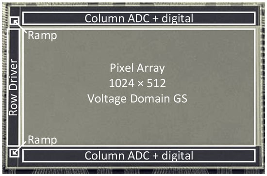
Figure 20.
The photograph of the CMOS image sensor.
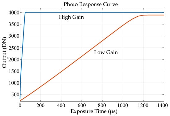
Figure 21.
Photo response curves captured at dual gain mode. (Blue: high gain response; Red: low gain response).
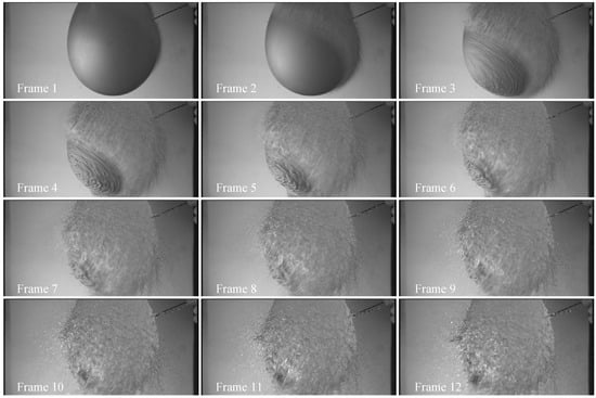
Figure 22.
Twelve consecutive frames captured at 1000 fps: piercing a water balloon (raw image).

Table 1.
Performance summary.
Table 2.
Power consumption measured at 1000 fps single gain mode under dark environment.
Table 3.
Performance comparison.
4. Discussion
In this paper, we presented a 1024 × 512 global shutter CMOS image sensor. The pixel was based on the voltage domain global shutter architecture, and the pitch was 24 μm × 24 μm. The frame rate was 1000 fps in single-gain mode and 500 fps in dual-gain mode. The combined dynamic range was 95 dB, and the full well capacity was 620 ke-. We analyzed the pixel noise performance, the non-linearity, and the image lag that originated from the parasitic capacitance within the pixel. A 10T pixel with dual gain channels was implemented to relax the requirements for the readout circuit. The parasitic capacitances in the pixel were smaller than 0.01 fF to minimize lag and non-linearity.
The ramp generator was based on a 12-bit full thermometer code current-steering DAC with high driving capability. We analyzed the non-linear response phenomenon of the ramp. The length of the ramp bus was approximately 2.46 cm. Theoretically, this architecture can be used in a stitched CIS. A static comparator with a current compensation block was also discussed. The noise from the pixel source follower, column current source, column ramp buffer, and the comparator itself was analyzed, which can guide the design of low-noise readout.
Author Contributions
CIS architecture, pixel, PC driver, column readout, ramp generator and writing: L.H.; top-level simulation and ESD: G.C.; column counter and row driver: G.W.; digital: X.Z., R.Z. and W.F.; pixel: W.P. and G.Y.; measurement: Y.Y. and D.W.; ramp: S.M.; bandgap: S.W. and B.F.; sub-LVDS: H.B.; PLL: L.D.; project administration: R.C. All authors have read and agreed to the published version of the manuscript.
Funding
This research received no external funding.
Institutional Review Board Statement
Not applicable.
Informed Consent Statement
Not applicable.
Data Availability Statement
The original contributions presented in this study are included in the article. Further inquiries can be directed to the corresponding author.
Conflicts of Interest
The authors declare no conflicts of interest.
References
- Meynants, G.; Beeckman, G.; Van Wichelen, K.; De Ridder, T.; Koch, M.; Schippers, G.; Bonnifait, M.; Diels, W.; Bogaerts, J. Backside illuminated 84 dB global shutter image sensor. In Proceedings of the International Image Sensors Workshop (IISW), Vaals, The Netherlands, 8–11 June 2015. [Google Scholar]
- Shike, H.; Kuroda, R.; Kobayashi, R.; Murata, M.; Fujihara, Y.; Suzuki, M.; Harada, S.; Shibaguchi, T.; Kuriyama, N.; Hatsui, T.; et al. A global shutter wide dynamic range soft X-ray CMOS image sensor with backside illuminated pinned photodiode, two-stage lateral overflow integration capacitor, and voltage domain memory bank. IEEE Trans. Electron Devices 2021, 68, 2056–2063. [Google Scholar] [CrossRef]
- Velichko, S. Overview of CMOS global shutter pixels. IEEE Trans. Electron Devices 2022, 69, 2806–2814. [Google Scholar] [CrossRef]
- Sakakibara, M.; Ogawa, K.; Sakai, S.; Tochigi, Y.; Honda, K.; Kikuchi, H.; Wada, T.; Kamikubo, Y.; Jyo, N.; Hayashibara, R.; et al. A back-illuminated global-shutter CMOS image sensor with pixel-parallel 14b subthreshold ADC. In Proceedings of the 2018 IEEE International Solid-State Circuits Conference (ISSCC), San Francisco, CA, USA, 11–15 February 2018; pp. 80–81. [Google Scholar]
- Lee, J.; Kim, S.; Baek, I.; Shim, H.; Kim, T.; Kim, T.; Kyoung, J.; Im, D.; Choi, J.; Cho, K.; et al. A 2.1e- temporal noise and −105 dB parasitic light sensitivity backside-illuminated 2.3 μm-pixel voltage-domain global shutter CMOS image sensor using high-capacity DRAM capacitor technology. In Proceedings of the 2020 IEEE International Solid-State Circuits Conference (ISSCC), San Francisco, CA, USA, 16–20 February 2020; pp. 102–105. [Google Scholar]
- Wang, X.; Bogaerts, J.; Vanhorebeek, G.; Ruythoren, K.; Ceulemans, B.; Lepage, G.; Willems, P.; Meynants, G. A 2.2M CMOS image sensor for high speed machine vision applications. In Proceedings of the SPIE 7536, Sensors, Cameras, and Systems for Industrial/Scientific Applications XI, San Jose, CA, USA, 25 January 2010. 75360M. [Google Scholar]
- Stark, L.; Raynor, J.M.; Lalanne, F.; Henderson, R.K. Back-illuminated voltage-domain global shutter CMOS image sensor with 3.75 µm pixels and dual in-pixel storage nodes. In Proceedings of the 2016 IEEE Symposium on VLSI Technology, Honolulu, HI, USA, 14–16 June 2016. [Google Scholar]
- Theuwissen, A.; Meynants, G. Welcome to the World of Single-Slope Column-Level Analog-to-Digital Converters for CMOS Image Sensors; Now Publishers: Norwell, MA, USA, 2021. [Google Scholar]
- Agarwal, A.; Hansrani, J.; Bagwell, S.; Rytov, O.; Shah, V.; Ong, K.; Blerkom, D.; Bergey, J.; Kumar, N.; Lu, T.; et al. A 316 MP, 120fps, high dynamic range CMOS image sensor for next generation immersive displays. Sensors 2023, 23, 8383. [Google Scholar] [CrossRef] [PubMed]
- Levski, D.; Wäny, M.; Choubey, B. Ramp noise projection in CMOS image sensor single-slope ADCs. IEEE Trans. Circuits Syst. I Regul. Pap. 2017, 64, 1380–1389. [Google Scholar] [CrossRef]
- Meynants, G.; Wolfs, B.; Bogaerts, J.; Li, P.; Li, Z.; Li, Y.; Creten, Y.; Ruythooren, K.; Francis, P.; Lafaille, R.; et al. A 47 Mpixel 36.4 × 27.6 mm2 30 fps global shutter image sensor. In Proceedings of the International Image Sensors Workshop (IISW), Hiroshima, Japan, 30 May–2 June 2017. [Google Scholar]
- Guo, Z.; Li, L.; Xu, R.; Liu, S.; Yu, N.; Yang, Y.; Wu, L. High consistency ramp design method for low noise column level readout chain. Sensors 2024, 24, 7057. [Google Scholar] [CrossRef] [PubMed]
- Imai, K.; Yasutomi, K.; Kagawa, K.; Kawahito, S. A distributed ramp signal generator of column-parallel single-slope ADCs for CMOS image sensors. IEICE Electron. Exp. 2012, 9, 1893–1899. [Google Scholar] [CrossRef]
- Nie, K.; Zha, W.; Shi, X.; Li, J.; Xu, J.; Ma, J. A single slope ADC with row-wise noise reduction technique for CMOS image sensor. IEEE Trans. Circuits Syst. I Regul. Pap. 2020, 67, 2873–2882. [Google Scholar] [CrossRef]
- Liu, Q.; Edward, A.; Kinyua, M.; Soenen, E.G.; Silva-Martinez, J. A low-power digitizer for back-Illuminated 3-D-stacked CMOS image sensor readout with passing window and double auto-zeroing techniques. IEEE J. Solid State Circuits 2017, 52, 1591–1604. [Google Scholar] [CrossRef]
- Sepke, T.; Holloway, P.; Sodini, C.G.; Lee, H. Noise analysis for comparator-based circuits. IEEE Trans. Circuits Syst. I Regul. Pap. 2009, 56, 541–553. [Google Scholar] [CrossRef]
- Wang, F.; Han, L.; Theuwissen, A. Development and evaluation of a highly linear CMOS image sensor with a digitally assisted linearity calibration. IEEE J. Solid-State Circuits 2018, 53, 2970–2981. [Google Scholar] [CrossRef]
- GSPRINT6502BSI—6.5 µm 2 MP Global Shutter CMOS Image Sensor. Available online: https://www.gpixel.com/en/pro_details_11266.html (accessed on 1 July 2025).
- CAE302 “ELOIS” High Dynamic Range, 2048×256 Pixel, Rad-Hard. Available online: https://caeleste.be/wp-content/uploads/2021/03/ELOIS-Leaflet.pdf (accessed on 1 July 2025).
Disclaimer/Publisher’s Note: The statements, opinions and data contained in all publications are solely those of the individual author(s) and contributor(s) and not of MDPI and/or the editor(s). MDPI and/or the editor(s) disclaim responsibility for any injury to people or property resulting from any ideas, methods, instructions or products referred to in the content. |
© 2025 by the authors. Licensee MDPI, Basel, Switzerland. This article is an open access article distributed under the terms and conditions of the Creative Commons Attribution (CC BY) license (https://creativecommons.org/licenses/by/4.0/).