


Time-Domain ADC and Security Co-Design for SiP-Based Wireless SAW Sensor Readers


Abstract
1. Introduction
- (1)
- In a SiP-based Multiprocessor System-on-Chip (MPSoC), this work presents the first implementation of a time-domain ADC in the programmable logic (PL) to process transient periodic echo signals from SAW sensors. Meanwhile, the processing system (PS) generates real-time graphical web browser interfaces that dynamically update the processed data. Compared to previous acquisition systems, this approach integrates sampling, signal processing, and visualization into a unified framework, eliminating the need for application in PC and dedicated hardware.
- (2)
- The time-domain ADC eliminates the need for external ADC circuits and peripheral components. Additionally, SiP integration reduces the system volume and weight compared to the original system, achieving a more compact and lightweight design while maintaining functional integrity.
- (3)
- Conventional IoT systems typically require additional hardware resources to enhance security. In contrast, this work integrates ADC sampling with a PUF challenge–response mechanism through a novel approach. During TDC calibration, the system exploits the inherent randomness of FPGA carry chain propagation delays to generate a unique hardware fingerprint. This method eliminates the need for extra hardware components while achieving seamless security integration.
2. System Architecture
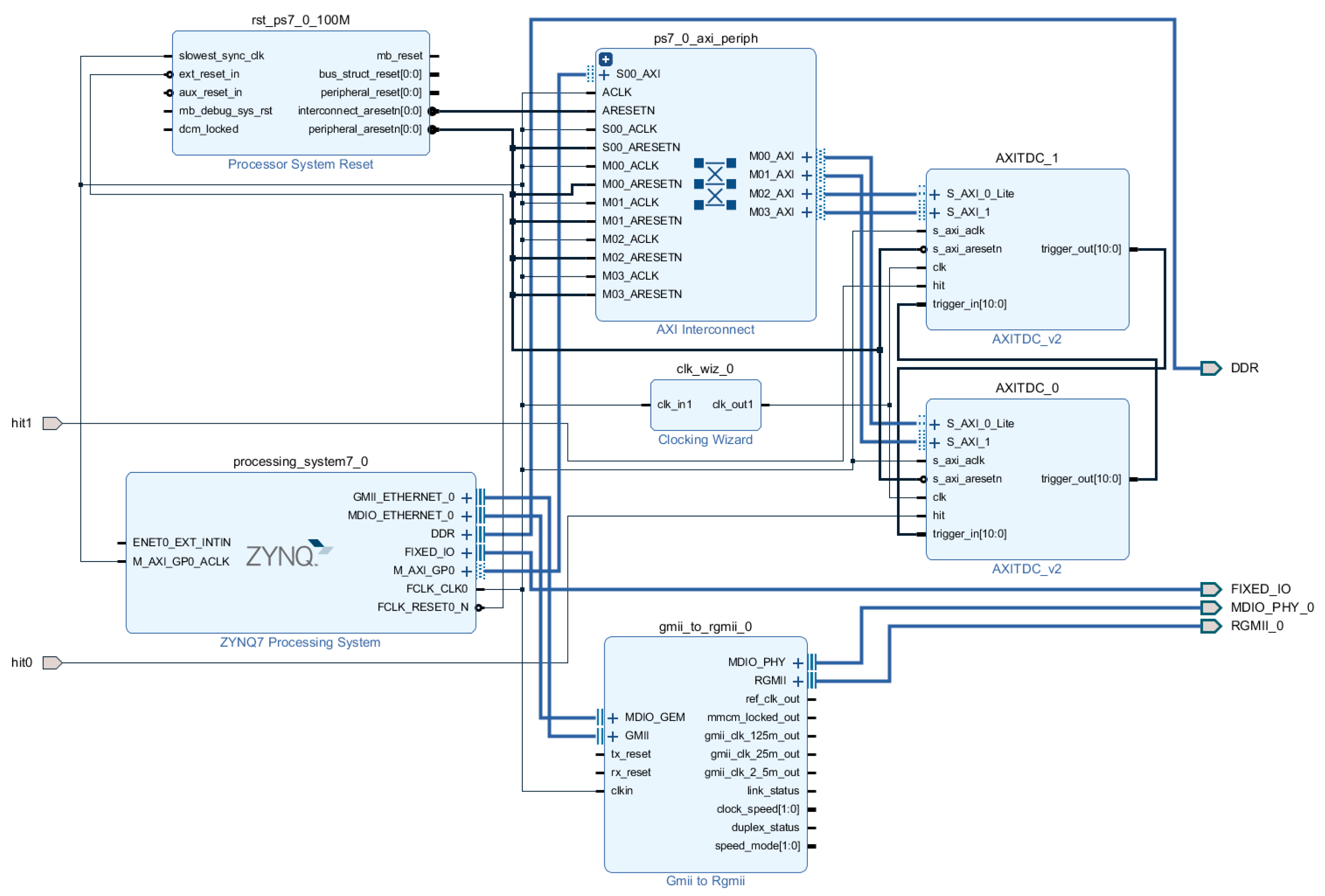
2.1. System Architecture and Work Process
2.2. Signal Analysis and Acquisition
2.2.1. Signal Characteristics at Resonance and Detuning
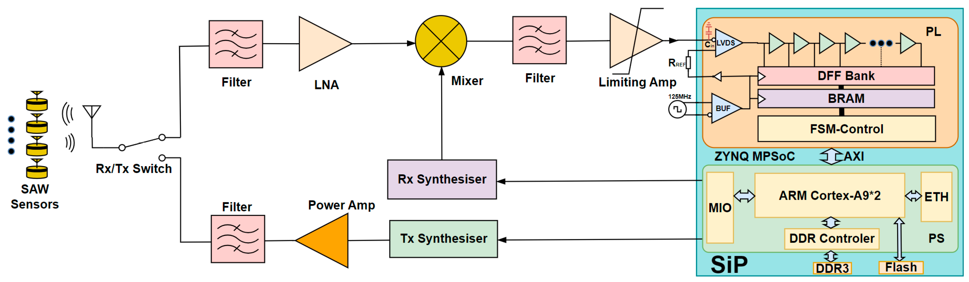
2.2.2. Design of RF Transceiver Front-End
2.3. SiP Implementation
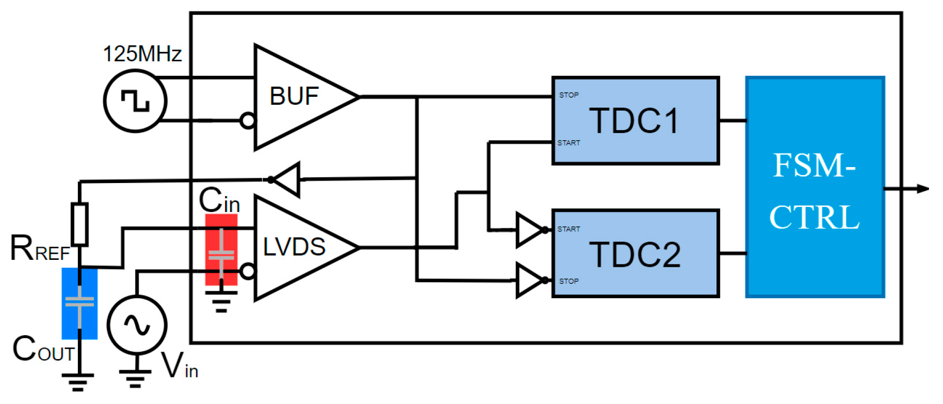
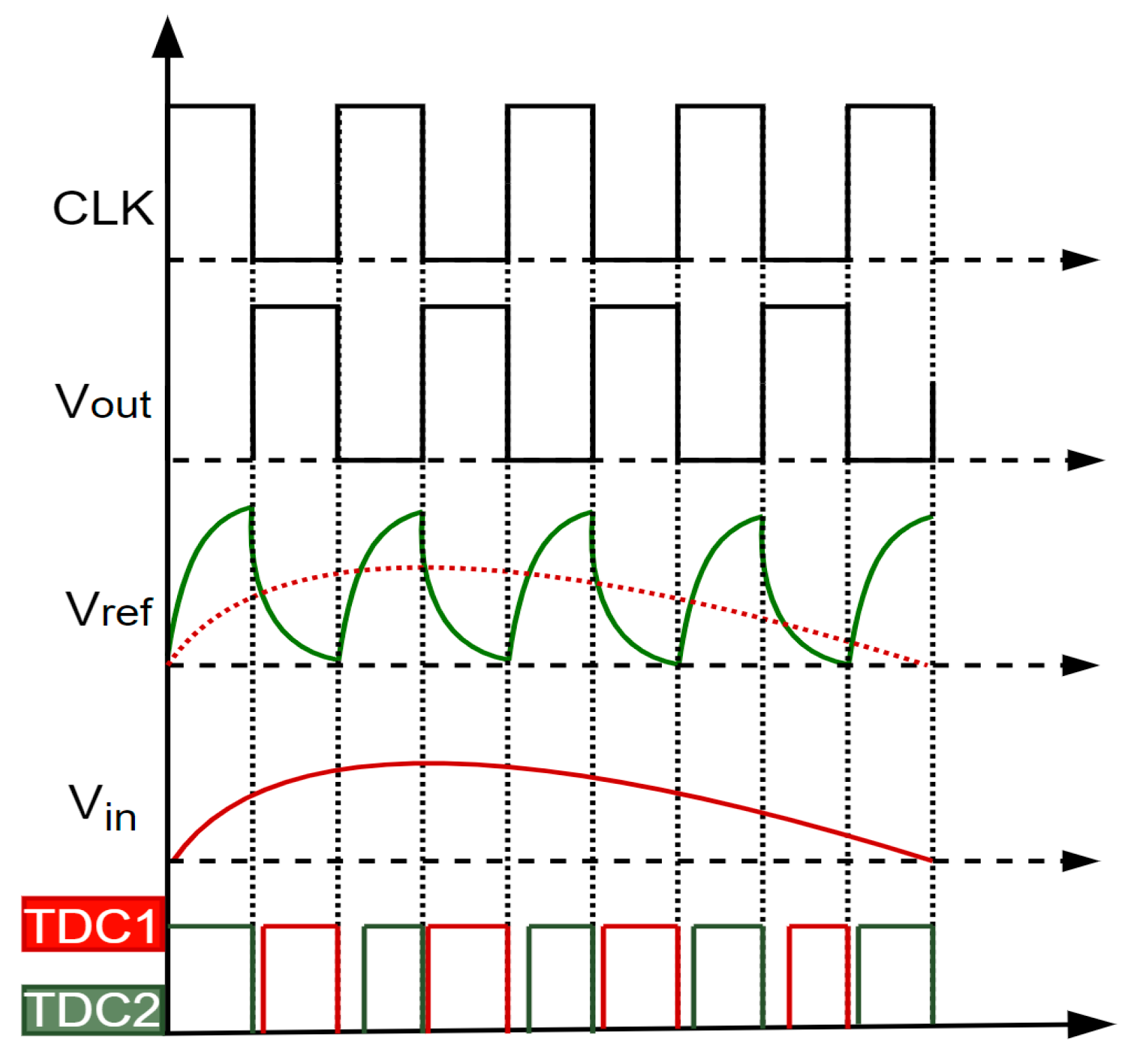
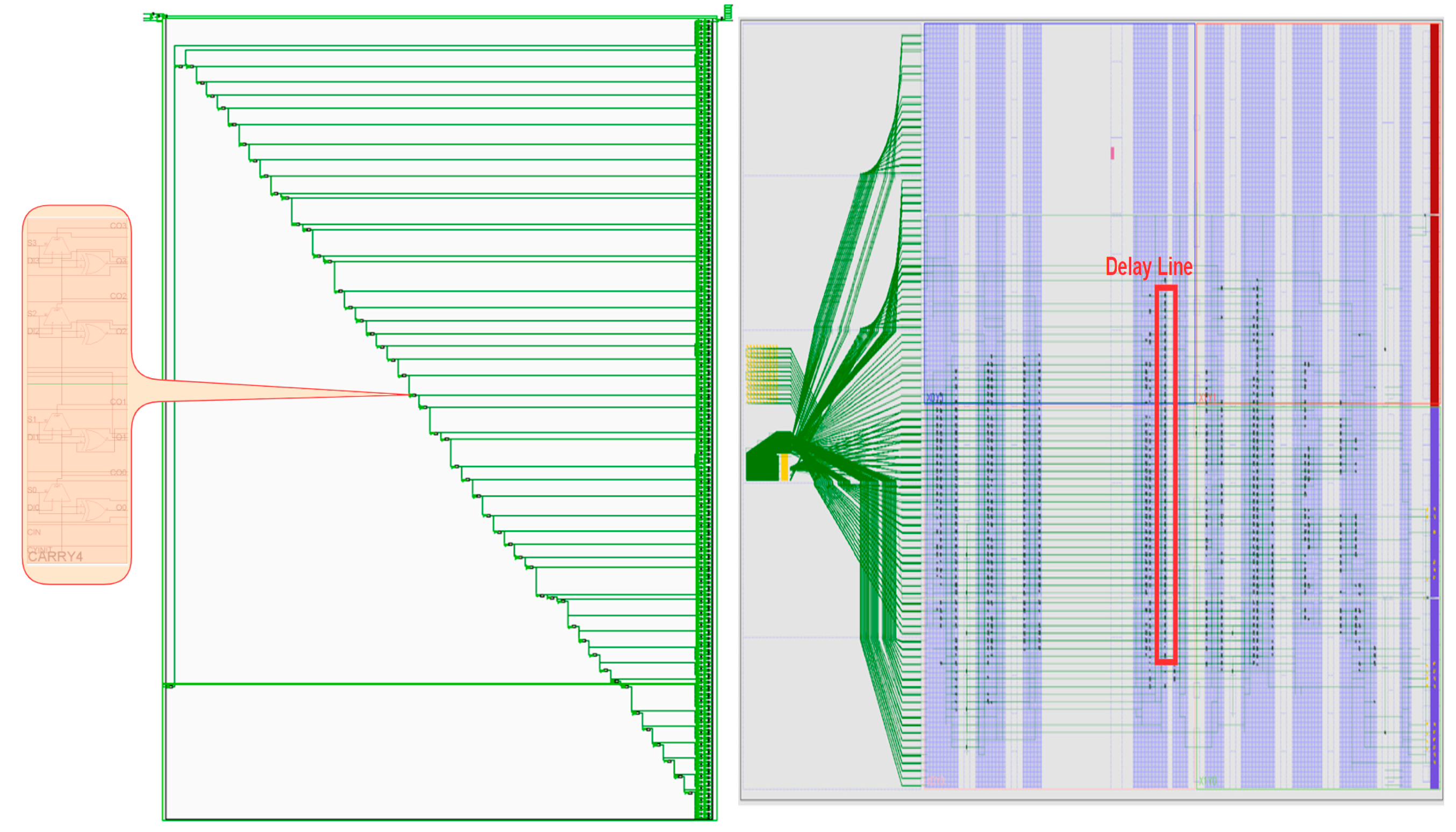
2.4. Time-Domain ADC Implementation in SiP
3. Delay Line Calibration and PUF Design in SiP
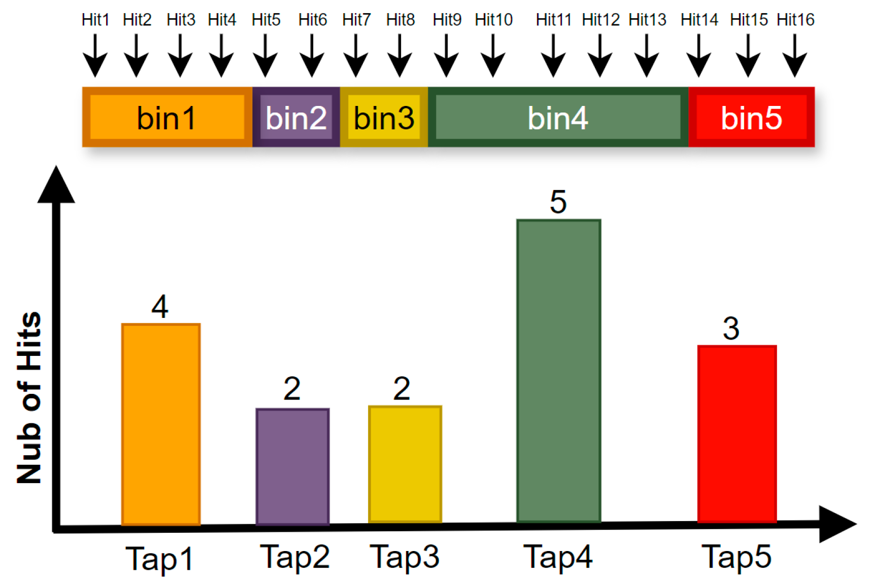
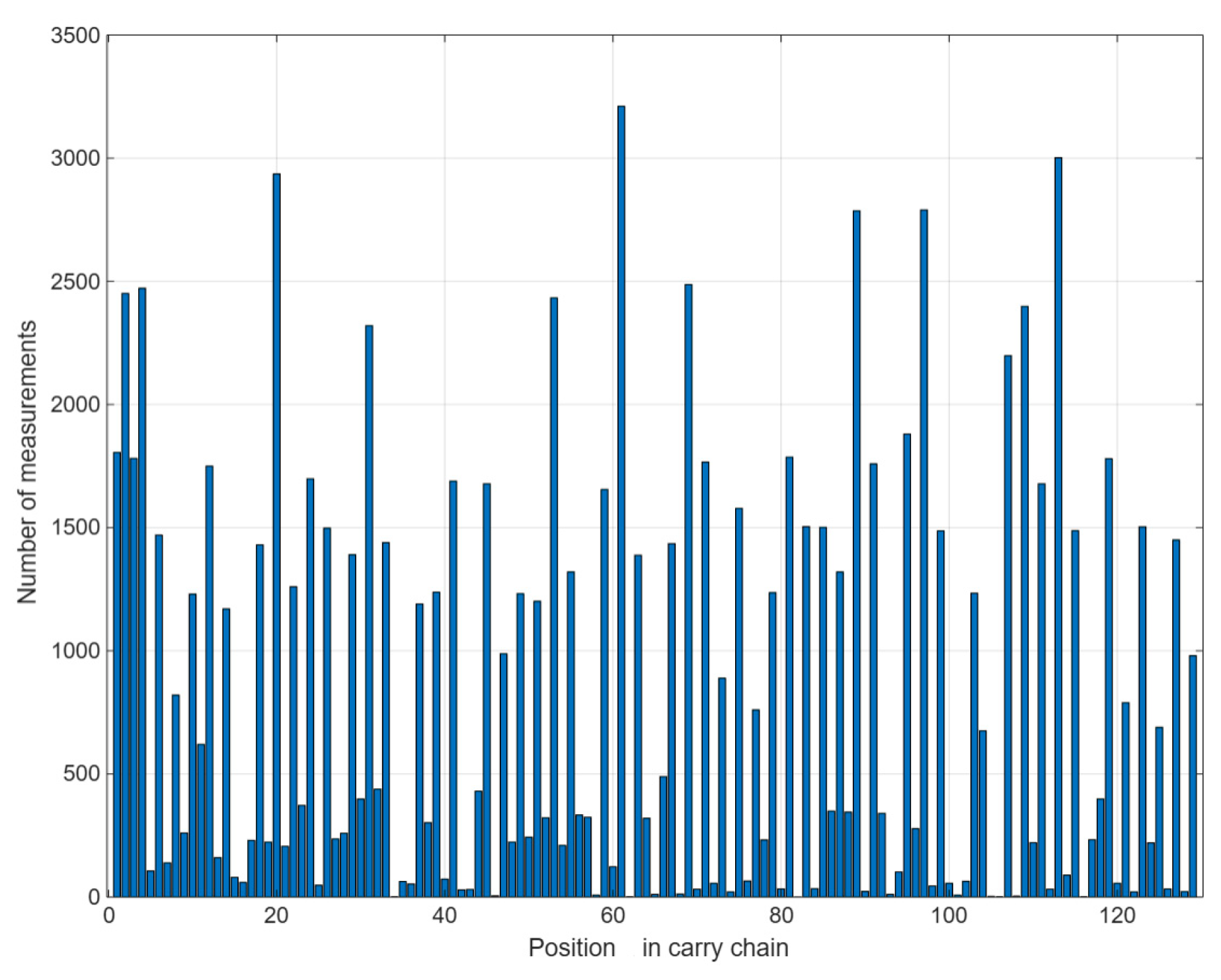
3.1. Code Density Analysis for Calibration
3.2. PUF Implementation While Calibrating
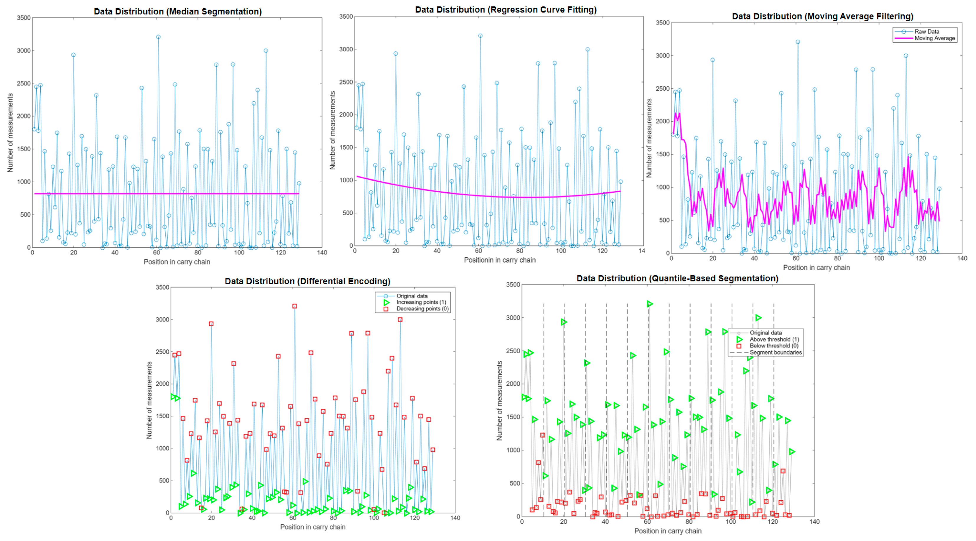
Binarization Segmentation Methods
- 1.
- Median Segmentation
- 2.
- Regression Curve Fitting
- 3.
- Moving Average Filtering
- 4.
- Differential Encoding
- 5.
- Quantile-Based Segmentation
4. Results
4.1. ADC Performance and Effective Number of Bits
4.2. PUF Characteristic Analysis Results
4.2.1. Reliability Results
4.2.2. Uniformity Results
4.2.3. Uniqueness Results
5. Discussion
Author Contributions
Funding
Institutional Review Board Statement
Informed Consent Statement
Data Availability Statement
Acknowledgments
Conflicts of Interest
References
- Li, Y.; Yang, G.; Cao, L.; Jiang, B.; Ji, X. Research of SAW Temperature and Pressure Dual Parameter Measuring Sensor Based on Delay Line Type. Instrum. Exp. Tech. 2020, 63, 707–715. [Google Scholar] [CrossRef]
- Rodríguez-Madrid, J.G.; Iriarte, G.F.; Williams, O.A.; Calle, F. High Precision Pressure Sensors Based on SAW Devices in the GHz Range. Sens. Actuators A Phys. 2013, 189, 364–369. [Google Scholar] [CrossRef]
- Zhgoon, S.; Shvetsov, A.; Ancev, I.; Bogoslovsky, S.; Sapozhnikov, G.; Trokhimets, K.; Derkach, M. SAW Temperature Sensor on Quartz. IEEE Trans. Ultrason. Ferroelectr. Freq. Control. 2015, 62, 1066–1075. [Google Scholar] [CrossRef]
- Gao, Z.; Wen, Y.; Xiao, Q.; Lei, H.; Wang, W.; Fan, Y. A High Performance Passive Wireless SAW Torque Sensor. IEEE Sens. J. 2025, 25, 18192–18200. [Google Scholar] [CrossRef]
- Zou, Y.; Zhao, Z.; Hu, F.; Cheng, L.; Xue, X.; Wang, W. High-Speed Reader for Contactless Resonant Surface Acoustic Wave Sensors. IEEE Trans. Instrum. Meas. 2024, 73, 6505609. [Google Scholar] [CrossRef]
- Pohl, A. A Review of Wireless SAW Sensors. IEEE Trans. Ultrason. Ferroelectr. Freq. Control. 2000, 47, 317–332. [Google Scholar] [CrossRef] [PubMed]
- Kalinin, V.; Beckley, J.; Makeev, I. High-Speed Reader for Wireless Resonant SAW Sensors. In Proceedings of the 2012 European Frequency and Time Forum, Gothenburg, Sweden, 23–27 April 2012; pp. 428–435. [Google Scholar] [CrossRef]
- Gao, Z.; Chen, Z.; Huang, X.; Tong, R.; Wang, M. Design and Implementation of SAW Reader Receiving Circuit. In Proceedings of the 2013 Symposium on Piezoelectricity, Acoustic Waves, and Device Applications, Changsha, China, 25–27 October 2013; pp. 1–4. [Google Scholar] [CrossRef]
- Pan, Y.; Yan, C.; Gao, X.; Yang, J.; Guo, T.; Zhang, L.; Wang, W. A Passive Wireless Surface Acoustic Wave (SAW) Sensor System for Detecting Warfare Agents Based on Fluoroalcohol Polysiloxane Film. Microsyst. Nanoeng. 2024, 10, 4. [Google Scholar] [CrossRef] [PubMed]
- Chen, Z.; Jia, H.; Chen, T.; Wang, X.; Guo, J.; Cai, P. High-Speed Data Acquisition of the Reader of the SAW RFID System. IET Sci. Meas. Technol. 2019, 13, 1163–1169. [Google Scholar] [CrossRef]
- Chen, X.; Zhao, T.; Yu, B.; Zhou, Q. High Voltage Switch Cabinet Cable Chamber Temperature Monitoring Based on Acoustic Surface Wave and ZigBee. Gaoya Dianqi/High Volt. Appar. 2018, 54, 48–54. [Google Scholar] [CrossRef]
- Mao, Z.; Li, B.; Peng, L.; Zhang, Y. Design of Transponder for Wireless Resonant Temperature SAW Sensor. In Proceedings of the 2021 IEEE 6th International Conference on Signal and Image Processing (ICSIP), Nanjing, China, 22–24 October 2021; Volume 54, pp. 1210–1214. [Google Scholar] [CrossRef]
- Kerzerho, V.; Cauvet, P.; Bernard, S.; Azais, F.; Comte, M.; Renovell, M. A Novel DFT Technique for Testing Complete Sets of ADCs and DACs in Complex SiPs. IEEE Des. Test Comput. 2006, 23, 234–243. [Google Scholar] [CrossRef]
- Liu, B.-h.; Huang, J.-q. System-In-Package Technology for Miniaturization Design of Aero-Engine Electronic Control System. J. Aerosp. Power 2013, 28, 2140–2144. [Google Scholar]
- Wang, H.; Ma, J.; Yang, Y.; Gong, M.; Wang, Q. A Review of System-In-Package Technologies: Application and Reliability of Advanced Packaging. Micromachines 2023, 14, 1149. [Google Scholar] [CrossRef] [PubMed]
- Henzler, S. Time-to-Digital Converters; Springer: Dordrecht, The Netherlands, 2010; ISBN 9789048186273. [Google Scholar]
- Zhang, M.; Zhao, Y.; Chen, Y.; Crovetti, P.; Wang, Y.; Ning, X.; Qiao, S. A 7.4-Bit ENOB 600 MS/S FPGA-Based Online Calibrated Slope ADC without External Components. Sensors 2022, 22, 5852. [Google Scholar] [CrossRef] [PubMed]
- Nishimura, A.; Matsumoto, T.; Yonetsu, T.; Nakao, Y.; Fujita, S.; Maezawa, H.; Onishi, T.; Ogawa, H. Observational Demonstration of a Low-Cost Fast Fourier Transform Spectrometer with a Delay-Line-Based Ramp-Compare ADC Implemented on FPGA. Publ. Astron. Soc. Jpn. 2021, 73, 692–700. [Google Scholar] [CrossRef]
- Homulle, H.; Regazzoni, F.; Charbon, E. 200 MS/S ADC Implemented in an FPGA Employing TDCs. In Proceedings of the 2015 ACM/SIGDA International Symposium on Field-Programmable Gate Arrays, Monterey, CA, USA, 22–24 February 2015. [Google Scholar] [CrossRef]
- Khaddour, W.; Uhring, W.; Dadouche, F.; Dumas, N.; Madec, M. Calibration Methods for Time-To-Digital Converters. Sensors 2023, 23, 2791. [Google Scholar] [CrossRef] [PubMed]
- Rivoir, J. Fully-Digital Time-To-Digital Converter for ATE with Autonomous Calibration. In Proceedings of the 2006 IEEE International Test Conference, Santa Clara, CA, USA, 22–27 October 2006. [Google Scholar] [CrossRef]
- Mao, Z.; Li, B.; Peng, L.; Li, Y. Design and Implementation of IDELAY-RO PUF in Xilinx ZYNQ PSoCs. IEICE Electron. Express 2024, 21, 20240013. [Google Scholar] [CrossRef]
- Anandakumar, N.N.; Hashmi, M.S.; Sanadhya, S.K. Design and Analysis of FPGA-Based PUFs with Enhanced Performance for Hardware-Oriented Security. ACM J. Emerg. Technol. Comput. Syst. 2022, 18, 1–26. [Google Scholar] [CrossRef]
- Yu, M.D.; Sowell, R.; Singh, A.; M’Raïhi, D.; Devadas, S. Performance Metrics and Empirical Results of a PUF Cryptographic Key Generation ASIC. In Proceedings of the 2012 IEEE International Symposium on Hardware-Oriented Security and Trust, San Francisco, CA, USA, 3–4 June 2012. [Google Scholar] [CrossRef]
- Yan, W.; Jin, C.; Tehranipoor, F.; Chandy, J.A. Phase Calibrated Ring Oscillator PUF Design and Implementation on FPGAs. In Proceedings of the 2017 27th International Conference on Field Programmable Logic and Applications (FPL), Ghent, Belgium, 4–8 September 2017; pp. 1–8. [Google Scholar] [CrossRef]


| Data Set | 1805,2451,1781,2472,106,1473,139,821,260,1233,624,1753,162,1175,82,61,235,1432,223,2936,206,1261,372,1698,48,1498,236,259,1392,398,2324,438,1439,2,63,53,1190,302,1238,73,1689,29,31,430,1678,5,988,223,1232,243,1201,322,2433,217,1326,333,324,8,1655,123,3211,2,1388,320,11,489,1435,12,2487,32,1766,56,889,21,1578,65,761,232,1236,33,1786,1,1504,34,1501,349,1320,345,2786,23,1759,340,11,102,1880,278,2790,45,1487,56,8,64,1234,675,3,2,2198,4,2397,221,1676,32,3002,89,1488,2,233,398,1780,56,789,21,1503,224,689,33,1453,22,981 |
| Median Segmentation | 111101000101010001010101010010101000101010001010101010100010101000101010101000101010101010100010101000100010101010100010001000101 |
| Regression Curve Fitting 1 | 111101000101010001010101010010101000101010001010101010100010101000101010101010101010101010100010101000100010101010100010001000101 |
| Moving Average Filtering 2 | 010100000101010001010101010010101000101010001010101010100010101000101010101010101010101010100010101000110010101010100010101010101 |
| Differential Encoding | 10101010101010011010101010110101010101010111010101010100010101001101010101010101010101010100110101001100010101010101110101010101 |
| Quantile-Based Segmentation 3 | 111101000011010001010101010011111000101010011010101010110010101001101010101010101010101010110010101000110010111010100110101000101 |
| PUF | Uniformity | Uniqueness | Reliability | Response. Bit Length | Total Slices | Target FPGA |
|---|---|---|---|---|---|---|
| Anandakuma et al. [23] | 49.48 | 48.38 | 99.94 | 256 | 93 | Artix-7 |
| Zhang et al. [24] | 49.5 | 49.33 | 95.45 | 136 | 186 | Virtex-5 |
| Yan et al. [25] | 50.05 | N/A * | 99.33 | 128 | 647 | Artix-7 |
| CARRYs (Our work) | 53.28 | 49.43 | 97.56 | 128 ** | 32 | ZYNQ-7000 |
Disclaimer/Publisher’s Note: The statements, opinions and data contained in all publications are solely those of the individual author(s) and contributor(s) and not of MDPI and/or the editor(s). MDPI and/or the editor(s) disclaim responsibility for any injury to people or property resulting from any ideas, methods, instructions or products referred to in the content. |
© 2025 by the authors. Licensee MDPI, Basel, Switzerland. This article is an open access article distributed under the terms and conditions of the Creative Commons Attribution (CC BY) license (https://creativecommons.org/licenses/by/4.0/).
Share and Cite
Mao, Z.; Li, B.; Peng, L.; Wei, J. Time-Domain ADC and Security Co-Design for SiP-Based Wireless SAW Sensor Readers. Sensors 2025, 25, 4308. https://doi.org/10.3390/s25144308
Mao Z, Li B, Peng L, Wei J. Time-Domain ADC and Security Co-Design for SiP-Based Wireless SAW Sensor Readers. Sensors. 2025; 25(14):4308. https://doi.org/10.3390/s25144308
Chicago/Turabian StyleMao, Zhen, Bing Li, Linning Peng, and Jinghe Wei. 2025. "Time-Domain ADC and Security Co-Design for SiP-Based Wireless SAW Sensor Readers" Sensors 25, no. 14: 4308. https://doi.org/10.3390/s25144308
APA StyleMao, Z., Li, B., Peng, L., & Wei, J. (2025). Time-Domain ADC and Security Co-Design for SiP-Based Wireless SAW Sensor Readers. Sensors, 25(14), 4308. https://doi.org/10.3390/s25144308