1. Introduction
Printed circuit boards (PCBs) are an integral and indispensable component of electronic equipment, playing an exceptionally critical role in modern electronic technology. Their quality directly impacts the performance and reliability of the entire device [
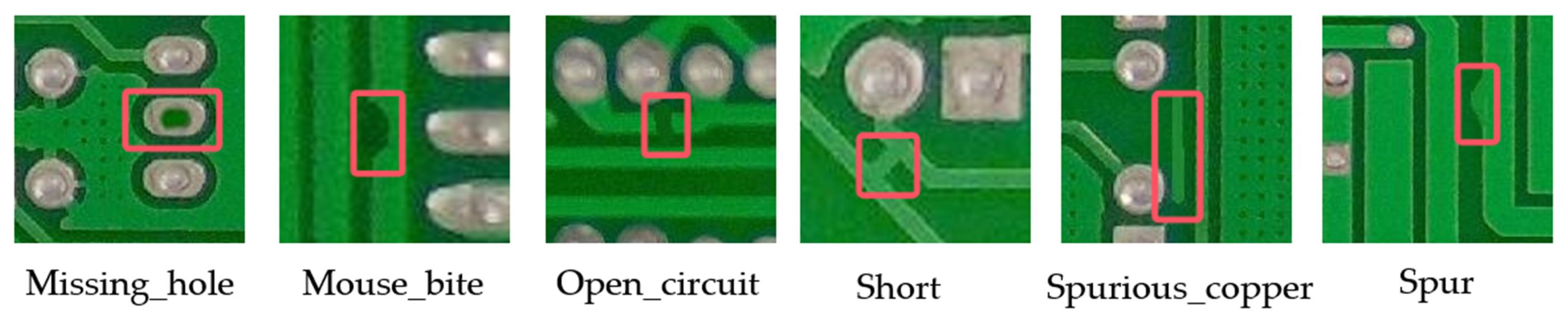
1]. Nonetheless, within the context of the PCB production process, due to complex manufacturing processes, external environmental disturbances, and operating errors, PCBs may have surface defects [
2] such as short circuits, missing holes, burrs, etc., which affect the normal use of electronic devices. Therefore, effective PCB defect detection is a critical and necessary step in ensuring that electronic equipment performs well and operates reliably.
In the current era of surging digitalization, technological development is undergoing rapid transformation. At the core of this transformation is deep learning, a field of artificial intelligence that is rapidly reshaping numerous industry patterns. In recent years, deep learning has achieved significant breakthroughs in the domain of computer vision [
3], especially in image recognition [
4], object detection [
5], and semantic segmentation. It has shown strong application potential and provides new ideas and methods for PCB defect detection. PCB defect detection methods based on deep learning can automatically mine and learn rich feature expressions [
6] from massive data, accurately identify and locate various types of defects on PCBs, significantly improve the accuracy and efficiency of detection, and promote the PCB inspection process towards intelligence and efficiency.
Classical deep learning models have played a crucial role in the development of PCB defect detection. AlexNet is the pioneer of modern deep learning-based image classification techniques, and was the first to demonstrate the power of deep neural networks in processing large-scale image data [
7]. Its success has inspired researchers to explore the application of deep learning in PCB defect detection. By utilizing its convolutional layer for feature extraction, it can identify some simple PCB defects to a certain extent. However, due to its relatively shallow architecture, it faces challenges in capturing complex defect features.
Subsequently, VGG was proposed to significantly deepen the network architecture [
8]. VGG’s convolutional layer stack has a small-size kernel, which allows for the extraction of more hierarchical and detailed features. In PCB defect detection, this allows for better identification of defects with complex shapes and textures. However, the large number of parameters in VGG leads to high computational cost and potential overfitting problems.
To solve the problem of deep network training, ResNet introduces residual structures [
9]. This innovation makes the training of ultra-deep networks independent of the gradient vanishing problem. In PCB defect detection, ResNet’s deep structure captures long-range dependencies and subtle defect features, greatly improving detection accuracy. In addition, its residual connectivity makes the model more robust and easier to train.
Over time, these classical models have been further optimized and adapted specifically for PCB defect detection. For example, the ensemble layer was modified to better preserve the spatial information associated with defect localization. The loss function was also adapted to better suit the characteristics of PCB defect datasets, e.g., to deal with class imbalance. These adjustments improve the performance of the classical deep learning-based PCB defect detection methods and lay a solid foundation for the subsequent development of more advanced detection algorithms.
Contemporary object detection architectures predominantly bifurcate into two methodological paradigms. The first category encompasses two-stage detectors [
10], exemplified by Faster RCNN frameworks. Recent advancements in this domain include Hu et al. [
11], who used a multi-scale feature re-identification technique based on Faster RCNN to identify defect optimized variants of PCB micro-defects, achieving a mAP of 94.2% in an industrial inspection scenario. Parallel developments by Ding et al. [
12] introduced TDD-Net, which integrates pyramid feature distillation with depthwise separable convolutions, establishing new benchmarks of 98.90% mAP on defect datasets. The second paradigm adopts single-stage detection mechanisms, prioritizing computational efficiency through unified regression pipelines. Notable implementations span SSD derivatives and YOLO evolutionary architectures. Wang et al. [
13] engineered a YOLOv3-based solder joint analyzer incorporating probability-density weighted anchor optimization, hybrid SE-CBAM attention fusion, and Focal-EIoU loss adaptation, achieving 96.69% mAP with 23 ms inference latency. Subsequent refinements by Liao et al. [
14] rearchitected YOLOv4’s backbone with Mish activation and Ghost modules, attaining 98.64% mAP alongside 41% parameter reduction. The YOLO architectural evolution continues with Lim’s [
15] YOLOv5 modification employing spatial-frequency attention in FPN pathways, effectively mitigating small-target feature dissipation, with 99% mAP in the experimental results. Chen’s team [
16] later proposed a YOLOv7 variant combining a FasterNet backbone with CBAM-enhanced neck structures, resolving the accuracy-efficiency tradeoff in high-throughput PCB inspection and achieving 99.2% mAP at 38 FPS. Most recently, Zhang et al. [
17] developed SF-YOLO through YOLOv8’s inspection head miniaturization, demonstrating 0.6% mAP@0.5 improvement with simultaneous 14.2% model compression and 17.2% parametric simplification.
Although significant advancements have been achieved in PCB defect detection research, persistent limitations in computational efficiency and generalizability to real-world industrial scenarios remain unresolved. Conventional CNN architectures, while achieving competitive detection precision, encounter deployment challenges in resource-limited industrial environments due to their substantial parameter sizes and intensive computational requirements. This constraint becomes particularly critical for embedded systems and mobile inspection terminals where hardware resources are strictly constrained. Existing improvements for the YOLO model introduce too many complex mechanisms to increase the detection precision, increase the network complexity and the number of parameters, and make sacrifices in computational cost. The objective is to further decrease the number of model parameters and resource consumption, all the while maintaining a high-precision detection rate for PCB defects. In particular, when it comes to small and intricate PCB surface defects, existing approaches face challenges in simultaneously taking into account detection precision, the quantity of model parameters, and the amount of model memory utilized.
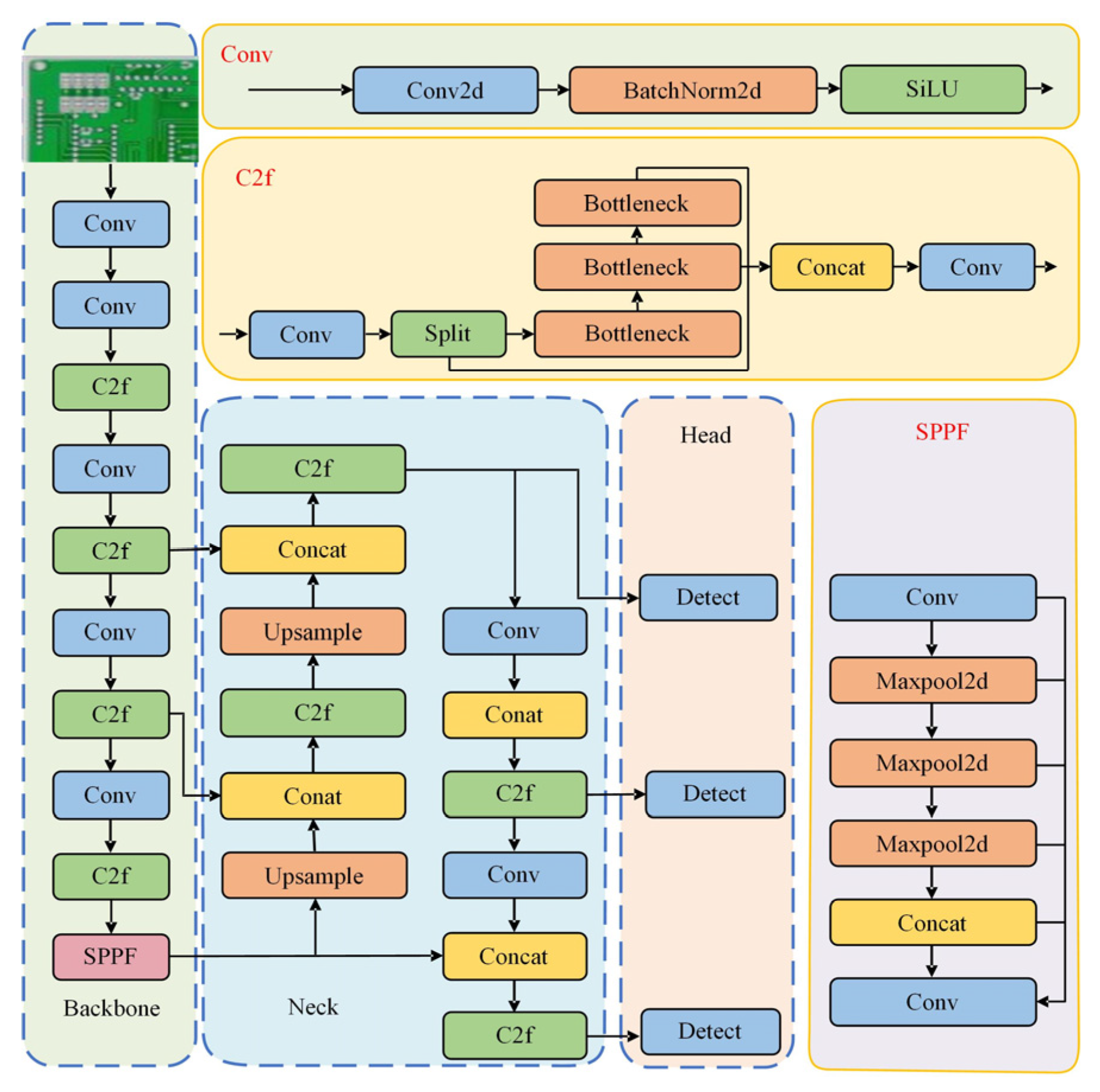
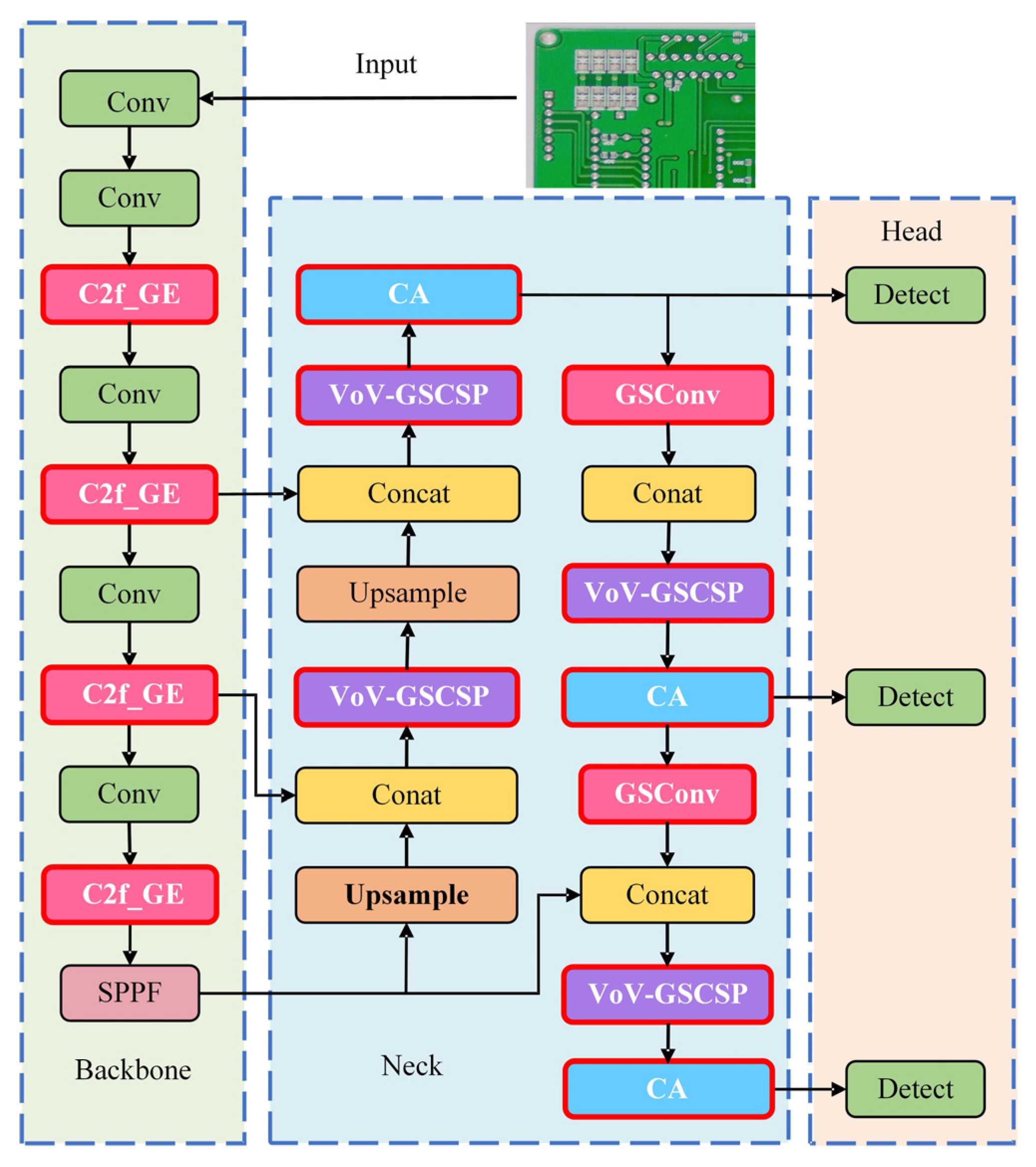
Among the many models, it is crucial to choose the right base model for improvement, and the YOLO series of models have become our focus due to their excellent performance in the field of target detection. Compared with the previous YOLOv5/6/7 versions, YOLOv8n has been optimized in terms of model structure, with lower computational complexity, higher detection accuracy, and improved detection of small targets. Compared to other alternative models, such as EfficientDet, RetinaNet, FCOS, etc., YOLOv8n has a simpler structural design, which makes it easier to customize and improve it for PCB defect detection tasks. For example, its unique module can quickly aggregate multi-scale features, which is highly suitable for PCB defects of different sizes. At the same time, YOLOv8n requires fewer computational resources to process images of the same resolution, making it more suitable for resource-constrained PCB inspection equipment. Combining these advantages, we choose YOLOv8n as the basis for improvement and propose the lightweight inspection algorithm GESC-YOLO, which aims to further optimize the model performance and reduce the number of model parameters and resource consumption while ensuring the inspection accuracy. GESC-YOLO is improved in the following three main aspects:
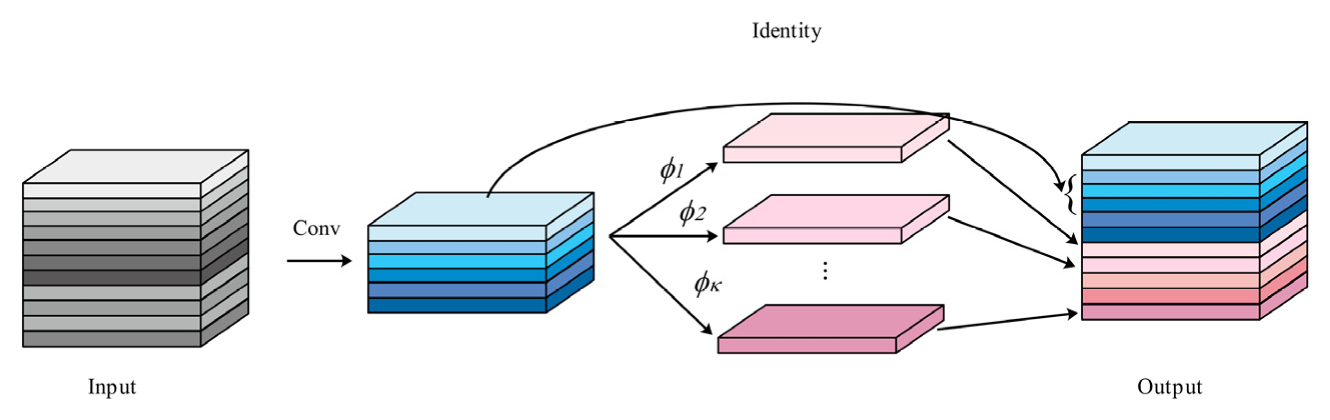
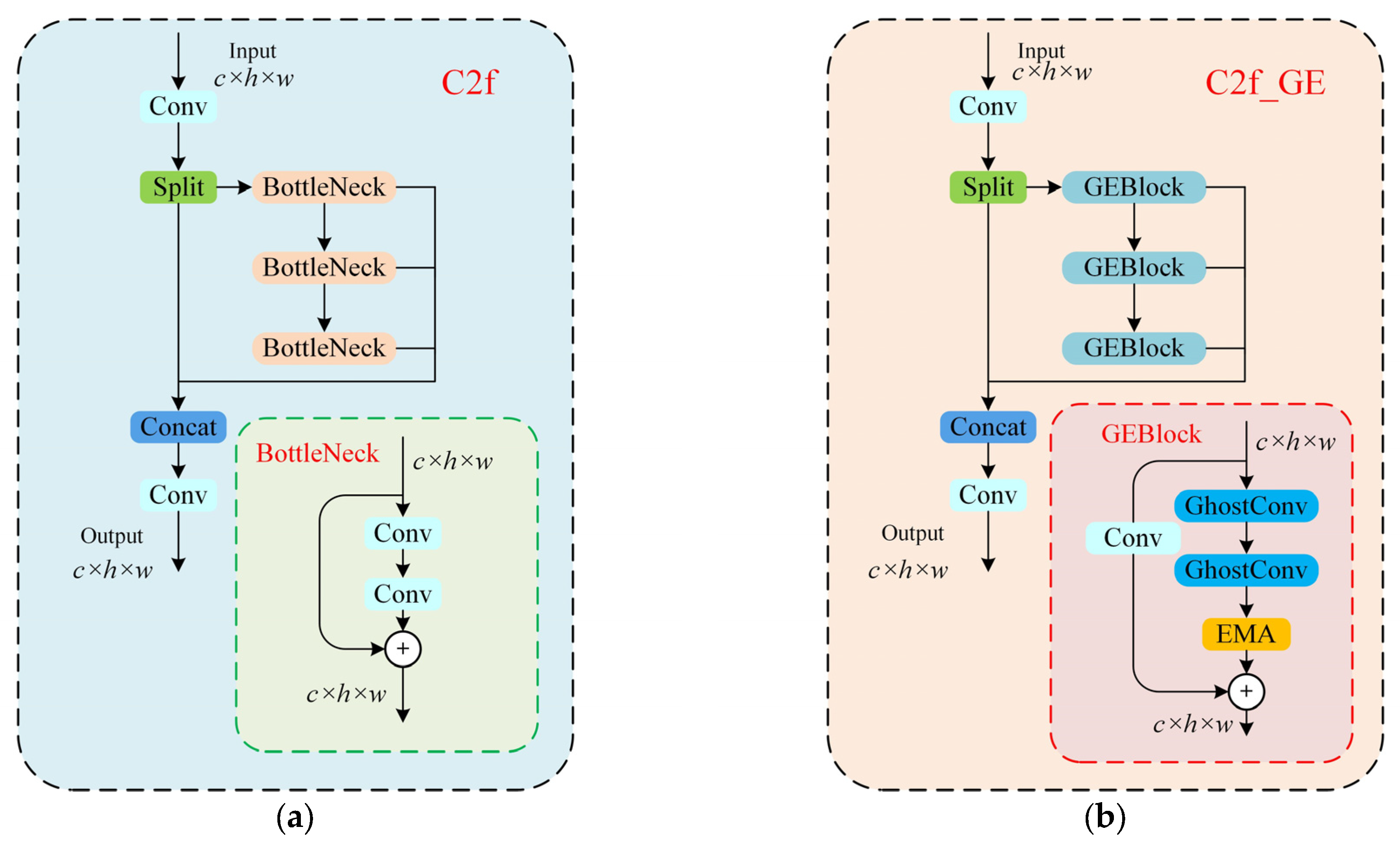
1. In the GESC-YOLO backbone network, a new lightweight module C2f-GE is designed to replace the original C2f module. This replacement offers several advantages. First, it effectively reduces computational complexity, enhancing the model’s efficiency in processing images and reducing its consumption of computational resources. Second, it causes an increase in the number of channels in the feature map, thereby improving the model’s capacity to recognize diverse types of PCB defects and enhancing its accuracy and generalization capability, ensuring successful performance when confronted with a range of complex PCB defect images.
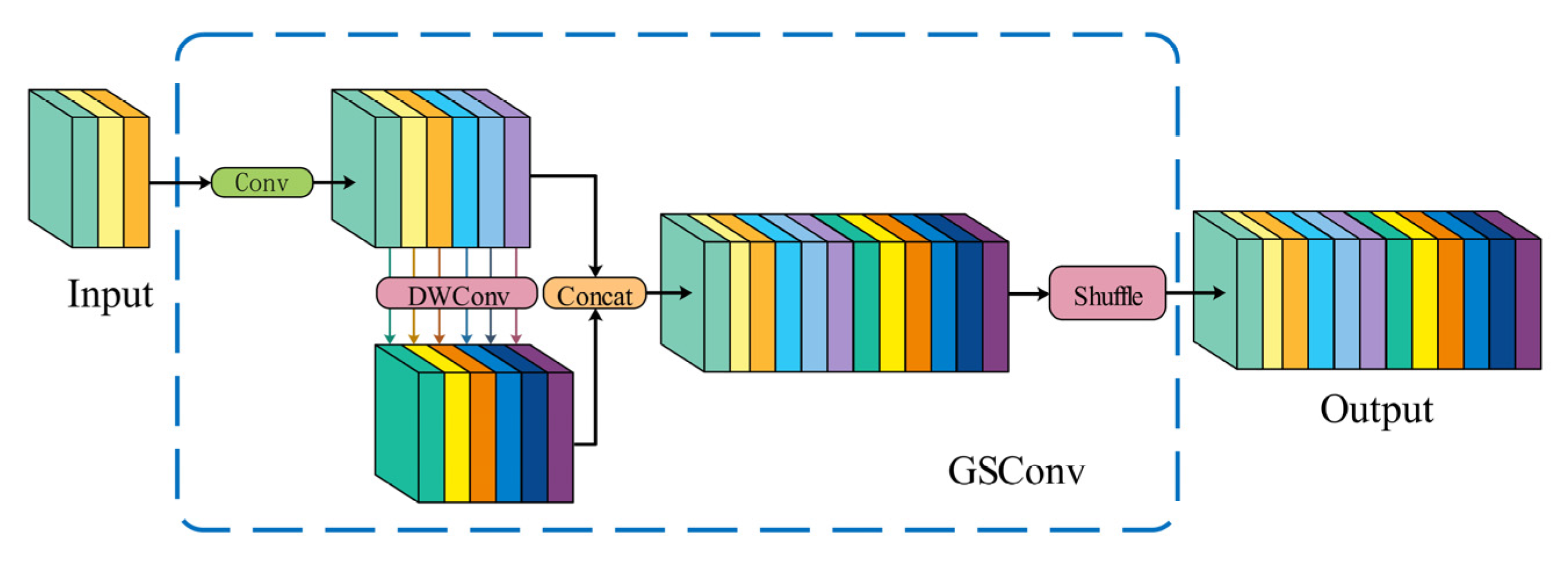
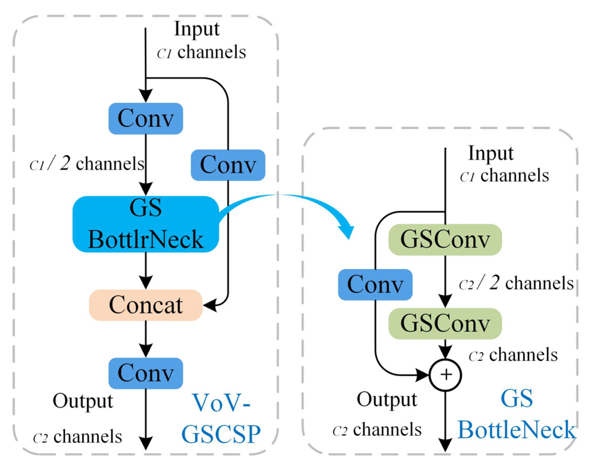
2. For the GESC-YOLO neck network, we construct a Slim-neck structure using a lightweight hybrid convolutional GSConv in combination with the VoV-GSCSP module. This structural design effectively augments the model’s discriminative capacity, facilitating precise identification of both micro-scale anomalies in printed circuit board inspection imagery. In addition, it successfully solves the problems of an excessive number of model parameters and a too-large model size, making the model more deployable and practical while maintaining high performance.
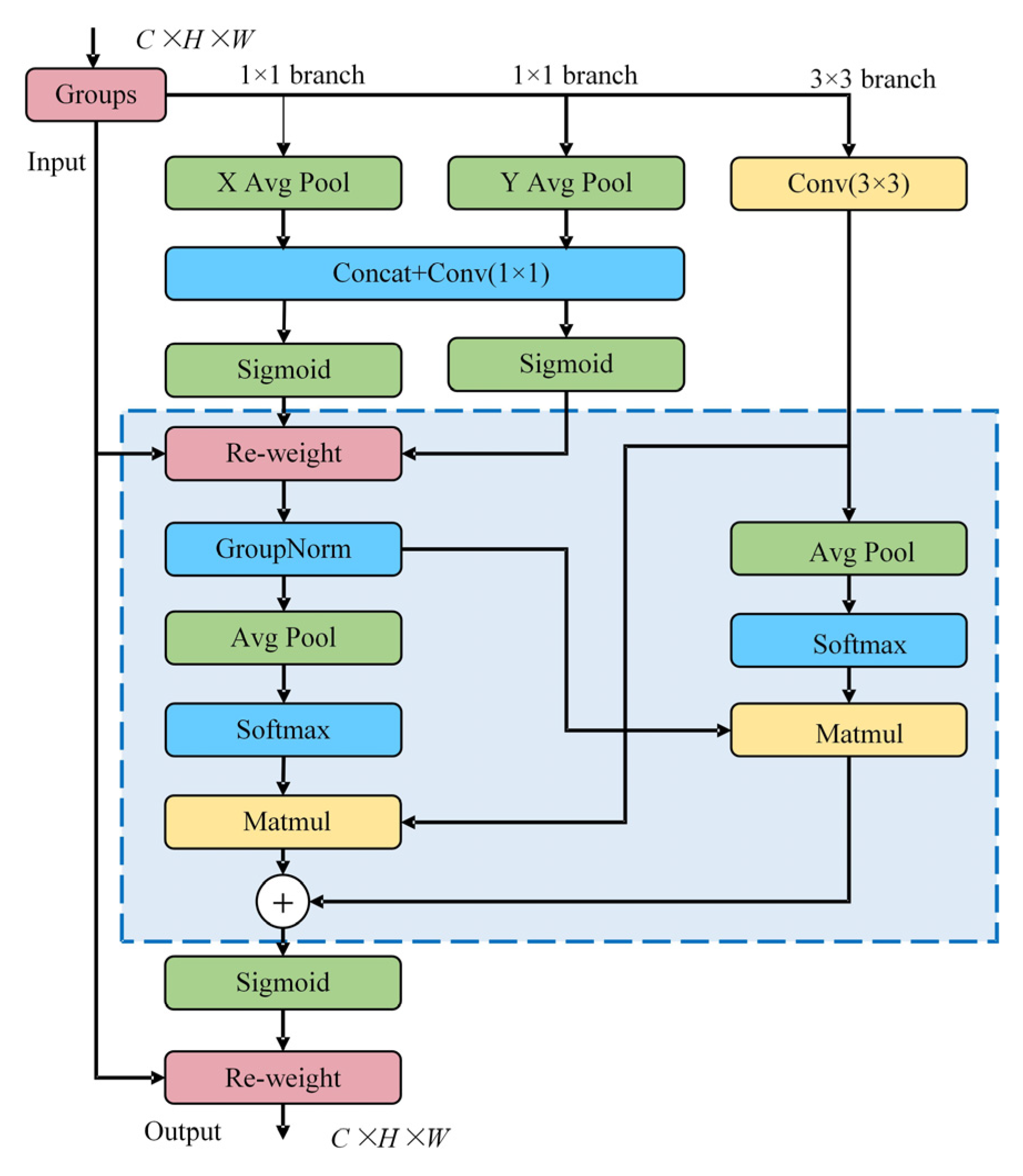
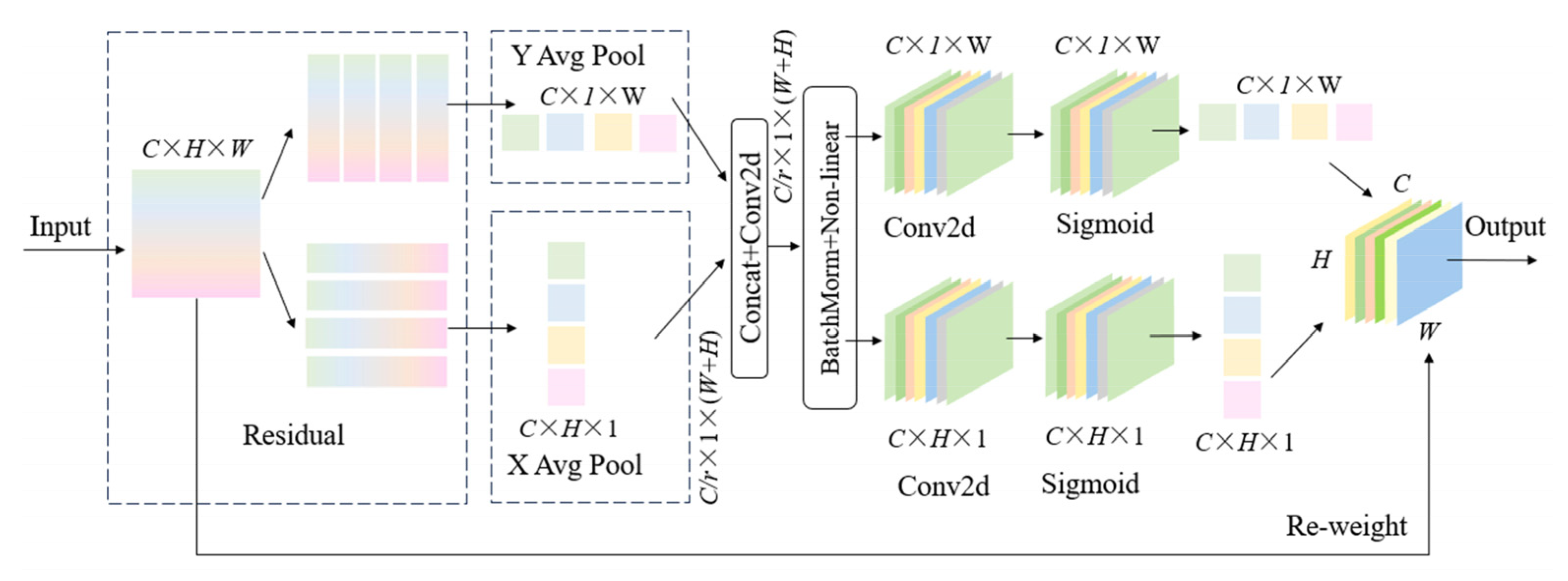
3. For the uniqueness of PCB defect images, coordinate attention is introduced in the neck network of GESC-YOLO. After the richer defect features are extracted from the previous C2f_GE module, CA can help the model to locate these features in the image more accurately, while the Slim-neck structure ensures that the model is lightweight while providing CA with a more effective representation of the features, which jointly improves the model’s detection and the localization accuracy of small defects. In summary, CA significantly improves the detection and localization accuracy of small defects. By modeling the spatial location information of the features more finely, the model can accurately locate them, thus effectively improving the detection performance. Even for small but complex PCB surface defects, GESC-YOLO ensures that the lightweight model’s detection performance is not compromised by its coordinate focus.
4. Experimental Results and Comparative Analysis
4.1. Ablation Experiment
To evaluate the optimization efficacy of the lightweight C2f_GE module, this study employs a controlled variable approach within the base model to comparatively analyze the performance of alternative lightweight architectures. The experimental results are shown in
Table 4.
According to the analysis of
Table 4, replacing the C2f with C2f_Ghost or C2f_Faster can improve the mAP@0.5 of the model and achieve lightweight status, but the precision of the model decreases by 0.4% and 0.1%, respectively, and the mAP@0.5:0.95 of the model decreases by 2.1% and 3.1%, respectively. When using the C2f_EMA module, the model size and parameter count increase while the precision decreases by 0.2%. When using the C2fCIB module, the precision, mAP@0.5, and mAP@0.5:0.95 decrease by 0.3%, 0.1%, and 0.5%, respectively. When using the C2f_GE module designed in this article, the precision and mAP are both improved by 0.1%, and the model size and parameters are reduced by 12.7% and 14%, respectively.
Since the C2f_Ghost module is constructed based on the lightweight idea of GhostNet and generates redundant feature maps through cheap operations, it retains a certain feature expression capability while reducing the amount of convolutional computation, and this design leads to a significant reduction in the number of model parameters. The better performance on the mAP@0.5 metric is because the metric has relatively loose requirements on the overlap between the detection frame and the real frame, and the C2f_Ghost module is able to identify the target effectively with lower precision requirements after quickly extracting the basic features, thus presenting a certain advantage in the mAP@0.5 evaluation.
The C2f_GE module integrates the GhostNet and EMA mechanisms and pays more attention to the effective fusion of multi-scale features and the richness of feature expression in its design. Although the number of parameters is slightly higher than that of C2f_Ghost, the cross-space interaction mechanism of EMA can guide the model to focus on key defective features, and it is far better than C2f_Ghost in mAP@0.5:0.95, which means that the C2f_GE module performs much better in locating and identifying defects, especially in the scenarios that require high detection accuracy. In addition, C2f_GE achieves the lowest level of computational resource consumption (FLOPS), which is 13.4% lower than that of the base model, which indicates that the module achieves a balance between accuracy and efficiency by optimizing the computational process and feature extraction method, which enhances the feature extraction capability while maintaining efficient computation.
The results conclusively demonstrate C2f_GE’s superiority in balancing parameters efficiency and detection precision. This can achieve model lightweighting while ensuring detection precision.
To further verify the effectiveness of each improvement module, a series of ablation experiments were designed and carried out. During the experiments, we adopted two different strategies: one is to add only one improvement module to the base model at a time to observe the effect of the module on the model performance; the other is to try to reasonably combine multiple improvement modules to explore the changes in the model’s performance under different combinations. Through such a comprehensive and detailed experimental setup, the effect of each improvement module and its combination can be precisely analyzed, which provides a strong basis for the optimization of the model. The experimental results are shown in
Table 5.
Analyzing the results in
Table 5, we can clarify the contribution of each component (C2f_GE, Slim-neck, CA) to the model performance improvement.
C2f_GE module: When the C2f_GE module alone is used to replace the original C2f module, the model precision (P) and mean average precision (mAP) are both improved by 0.1%. At the same time, the model size is reduced by 12.7% (from 6.3 M to 5.5 M), the number of parameters is reduced by 14% (from 3.01 × 10⁶ to 2.59 × 10⁶), and the computational effort (FLOPS) is reduced by 13.4% (from 8.2 G to 7.1 G). This shows that the C2f_GE module plays an important role in the backbone network. This module combines the ideas of GhostNet and EMA, which enables the model to extract key features more efficiently when processing images by reducing the computational complexity. GhostConv generates rich feature maps while reducing the computation, which provides the model with more information that may be used for identifying defects. EMA, on the other hand, performs multi-scale analysis of the input feature maps through its unique cross-space interaction mechanism, guiding the model to focus on critical defect areas in the PCB image. From the experimental results, the accuracy and mAP of the model are improved after using the C2f_GE module. This is because the C2f_GE module increases the number of channels of the feature map and enriches the feature representation, which enables the model to more accurately capture the subtle features of the defect, such as the irregularity of the edge of the defect and the contrast difference with the surrounding area and thus improves the identification and localization of the defect. In conclusion, the C2f_GE module effectively realizes model lightweighting, reduces the consumption of computational resources, improves the operation efficiency of the model, and at the same time improves the detection accuracy of the model.
Slim-neck structure: The Slim-neck structure, which consists of the GSConv and VoV-GSCSP modules, optimizes the feature fusion process in the neck network. GSConv effectively fuses different levels of feature maps through SC, DSC, and shuffle operations, reducing the computational scale while retaining the model’s detection accuracy. The VoV-GSCSP module, on the other hand, fully exploits the feature information through two different feature extraction methods, enhancing the model’s feature extraction capability. When detecting PCB defects, this structure can better integrate the different scales of features output from the backbone network, providing more representative features for the subsequent detection head. When used alone, the Slim-neck structure improves the model accuracy by 0.1% and the mAP@0.5 by 0.2%, reduces the model size by 9.5% (from 6.3 M to 5.7 M), cuts the number of parameters by 10% (from 3.01 × 10
6 to 2.71 × 10
6), and reduces the computation amount to 7.1 G. This indicates that the C2f_GE module can ensure the model detection accuracy while reducing the consumption of computational resources. From
Table 5, it can be seen that the mAP@0.5 of the model improves to 98.8% after using the Slim-neck structure. For ‘Open-Circuit’ defects, the Slim-neck structure can effectively integrate the information about the line direction and breakpoint features in different layers, enabling the model to more accurately judge whether there is a break in the line and improving the detection capability of these kinds of defects. In summary, the Slim-neck structure further optimizes the model structure and reduces the model complexity on the basis of ensuring the model detection accuracy, achieving a certain degree of lightweighting and improving the model performance.
Coordinate Attention (CA) Module: The Coordinate Attention (CA) Module, when introduced to the neck network, accurately analyses the spatial location information of features through axis-parallel feature encoding and dual-path processing. When detecting PCB defects, CA helps the model to more accurately locate the defects within the image. For instance, in the detection of ‘Mouse-Bite’ defects, CA leverages its unique mechanism to further spatially locate the features of these defects based on the rich features extracted by the C2f_GE module, enabling the model to more precisely identify the defect boundary and location information. When the CA module is introduced alone, it brings about notable improvements in model performance metrics. The precision of the model increases by 0.1%, the recall (R) improves by 0.3%, and mAP@0.5 rises by 0.2%. From the experimental results, these improvements indicate that CA is effective in enhancing the model’s accuracy in detecting and locating defects. In terms of model lightweighting, the model size and the number of parameters remain basically unchanged. This demonstrates that the CA module primarily serves to boost the model’s ability to locate and identify defect features, enhance its detection performance for small defects, and improve the overall detection accuracy without negatively impacting the model’s lightweight nature.
In summary, the C2f_GE, CA, and Slim-neck modules collaborate with each other to improve the model’s ability to reflect PCB defect features from different perspectives: the C2f_GE module enhances the feature extraction capability, the Slim-neck structure optimizes the feature fusion, and the CA improves the defect localization accuracy, which together make the GESC-YOLO model perform well in the PCB defect detection task. The C2f_GE module enhances the feature extraction capability, the Slim-neck structure optimizes the feature fusion, and the CA improves the localization accuracy.
When the three modules are used simultaneously, the accuracy of the model is improved by 0.3%, the mAP reaches 99.0%, which is improved by 0.4%, the size of the model is reduced by 25.4% (from 6.3 M to 4.7 M), the number of parameters is reduced by 28.6% (from 3.01 × 10⁶ to 2.15 × 10⁶), and the computation amount is reduced by 26.8% (from 8.2 G to 6.0 G). The three modules complement each other and play a complementary advantage, which significantly improves the detection accuracy while greatly realizing the light weight of the model and effectively enhancing the comprehensive performance of the model.
4.2. Comparative Experiments with Other Benchmark Models
To further substantiate the superiority of the lightweight algorithm GESC-YOLO proposed in this paper in comparison to other algorithms, comparative experiments were conducted, and the results are presented in
Table 6.
According to the analysis of
Table 6, it can be seen that the mAP of GESC-YOLO is significantly improved, and the model size and parameters are significantly reduced compared to Faster R-CNN and SSD. Compared with the YOLO series of lightweight networks YOLOv5n, YOLOv6n, and YOLOv7-tiny, the improved algorithm GESC-YOLO, while guaranteeing precision, has a mAP@0.5 that increased by 0.3%, 0.5%, and 0.3%, the model size is reduced by 11.3%, 45.9%, and 46.1%, and parameters are reduced by 14.3%, 49.2%, and 64.2%, respectively. Compared with the lightweight model YOLOv8n and large-scale model YOLOv8s of YOLOv8 series, the model size of the improved algorithm is reduced by 25.4% and 79.2%, respectively, the parameters are reduced by 28.6% and 80.6%, and the mAP reaches the highest rate of 99%. Compared with the latest models of YOLO series, YOLOv10n and YOLOv11n, the mAP is improved and the model size decreases by 18.9% and 20.3%, and parameters decrease by 14.5% and 16.7%, respectively. Under the metric of mAP@0.5:0.95, although YOLOv8s is higher than GESC-YOLO, the number of high parameters and resource consumption of the former does not meet the lightweight requirements. GESC-YOLO also reaches the lowest point under the metric of computational resource consumption (FLOPS). This advantage is especially prominent in resource-constrained industrial scenarios, bringing a new breakthrough in the practical application of PCB defect detection technology. It can be concluded that the advantage of the GESC-YOLO algorithm proposed in this paper lies in the significant reduction of the number of parameters, model size, and computational resource consumption while ensuring the detection precision. It performs better in terms of lightness and achieves the highest detection precision with the smallest model size. For resource-limited devices, it can deploy models more simply and efficiently, reducing storage pressure and runtime resource consumption with high efficiency and super-priority.
A comparison of experimental results for various types of defects before and after the improvement is shown in
Table 7.
As shown in
Table 7 above, GESC-YOLO (ours) significantly outperforms YOLOv8n (base) in several key metrics, demonstrating excellent detection performance. In terms of average precision (AP), GESC-YOLO (ours) achieves an overall AP value of 98.3%, which is higher than the 98.0% of YOLOv8n (base), and achieves accuracy improvement in Missing-Hole, Mouse-Bite, Open-Circuit, and Short categories of detection. Under this mAP@0.5 indicator, GESC-YOLO (ours) outperforms YOLOv8n’s (base) 98.6% with an average value of 99.0%, and the advantage is especially obvious in the Mouse-Bite, Short, and Spurious-Copper categories, which demonstrates that it possesses a more accurate target localization capability at lower intersection-to-parallel ratio (IoU) thresholds.
In a rigorous evaluation of mAP@0.5:0.95, a composite IoU threshold, the average score of GESC-YOLO (ours) of 64.3% is also higher than that of the control model of 63.8%. Although there are slight fluctuations in individual categories, it still maintains the lead in key categories such as Missing-Hole, Mouse-Bite, and Short, which highlights its detection stability and reliability in complex scenes. The above results fully confirm that GESC-YOLO (ours) effectively improves detection accuracy and generalization capability through innovative design and has significant advantages in PCB defect vision inspection tasks.
4.3. Visualization and Comparison of Experimental Results
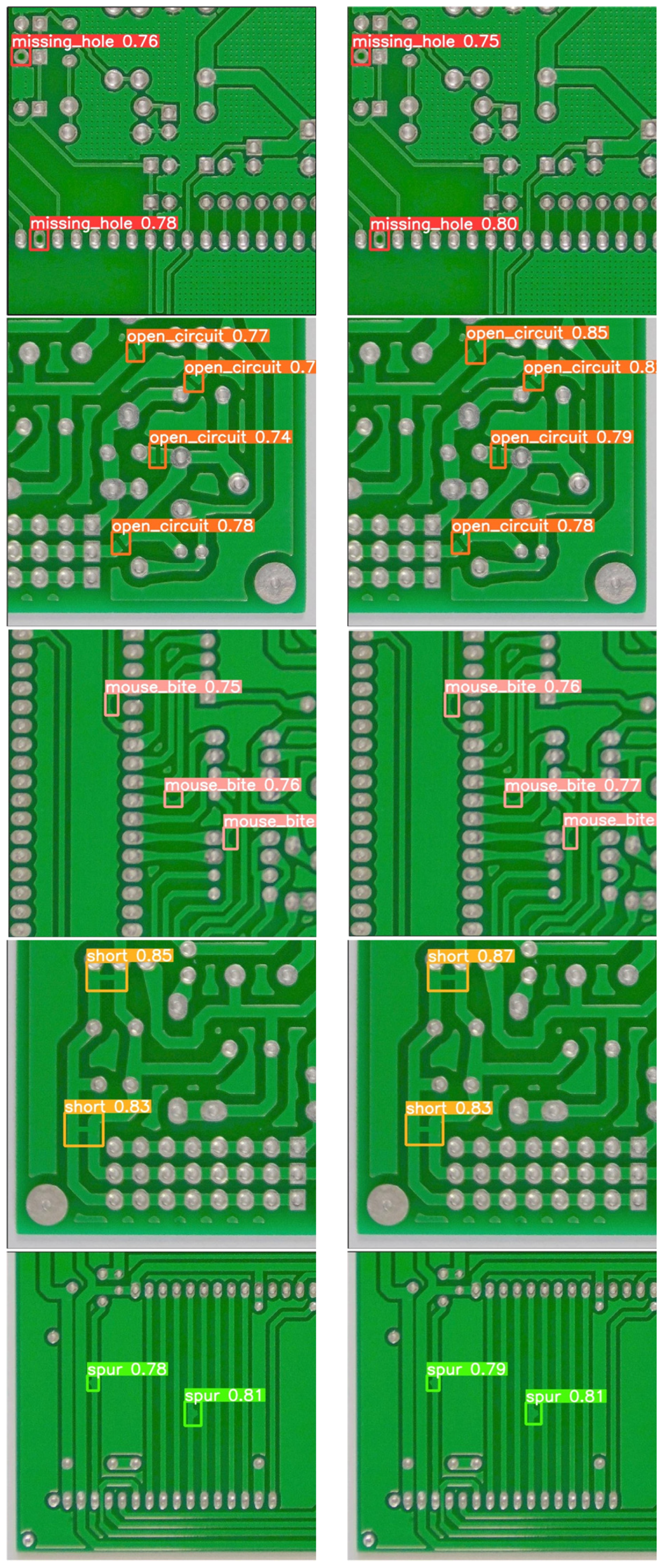
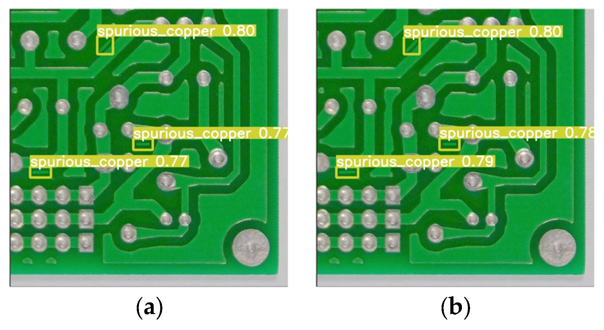
To evaluate the detection efficacy of the proposed GESC-YOLO algorithm, six different defects were selected for comparison with the original YOLOv8n. A comparison of the detection results of the original YOLOv8n and the lightweight model GESC-YOLO is shown in
Figure 11.
From the analysis of the detection results in
Figure 11, it can be seen that the lightweight model GESC-YOLO in this paper performs extremely well, correctly identified all six types of defects, and there is no problem of false or missed detections. For the detection of mouse_bite and short defects, our algorithm has similar detection performance to YOLOv8n, while for the detection of missing_hole, open_circuit, spurious_copper, and spur, our algorithm has slightly better detection performance than YOLOv8n. The above comparison results show that the GESC-YOLO proposed in this paper ensures and achieves improved detection performance while significantly reducing the number of parameters and the model size and can accurately detect defects on the PCB surface. This means that the lightweight improvement not only does not sacrifice the detection effect, but also exceeds the original model, which fully reflects the great value and effectiveness of lightweight improvement in practical applications.
4.4. Limitations and Future Work
Despite the promising results of the GESC-YOLO model in PCB defect detection, it has limitations. When handling non-high contrast defects, the model’s detection accuracy can be compromised as the low contrast makes it hard for the feature extraction modules to precisely identify defect features, potentially leading to missed or misclassified subtle defects. In industrial settings with various noise sources like electromagnetic interference and random pixel noise, the model’s performance suffers since it lacks a dedicated noise suppression mechanism, causing false or missed detections.
Moreover, our current evaluation metrics and model design do not fully account for scenarios where multiple defect types coexist within a single image. This can lead to an inaccurate interpretation of performance metrics such as mAP and recall, especially when dealing with complex defect combinations.
Another limitation is that our study has not comprehensively explored the impact of two important aspects on the model: the spatial resolution dependence and loss function design.
Regarding the spatial resolution dependence, we have not compared the performance of GESC-YOLO and other YOLO versions under different spatial resolutions in this paper. However, understanding the influence of spatial resolution is crucial for optimizing the model’s application. In future work, we will study the performance changes of the GESC-YOLO model at different spatial resolutions to identify the optimal range and improve its adaptability. We will also compare GESC-YOLO with other YOLO versions in terms of spatial resolution utilization to provide a basis for further model improvement.
Concerning loss function design, we used classical and well-established loss functions in this study, such as cross-entropy loss for classification and CIoU loss for regression. The focus of this research was on the impact of model architecture changes on performance, so we did not modify or innovate the loss functions. In future research, we plan to explore loss function design in depth and optimize it in combination with the model architecture proposed in this study to further improve the model’s performance.
For future work, we plan to develop more advanced feature extraction techniques, such as integrating state-of-the-art attention mechanisms or creating novel convolutional layers, to improve sensitivity to low-contrast features. Additionally, we aim to incorporate noise reduction algorithms into the model architecture or apply pre-processing denoising techniques to enhance the model’s robustness against industrial noise. Furthermore, we will focus on optimizing the evaluation strategies for scenarios with multiple defect types per image. This includes exploring more refined metric calculation methods, such as weighted averaging and category-specific evaluations, to better reflect the model’s performance in complex, real-world conditions. These efforts will further optimize the model’s detection performance and facilitate its practical deployment in industrial equipment.


