Article

A High-Gain Circularly Polarized Magnetoelectric Dipole Antenna Array for Millimeter-Wave Applications

1
School of Ocean Information Engineering, Jimei University, Xiamen 361000, China
2
College of Information Science and Engineering, Hohai University, Changzhou 213200, China
*
Authors to whom correspondence should be addressed.
These authors contributed equally to this work.
Sensors 2025, 25(10), 3046; https://doi.org/10.3390/s25103046
Submission received: 7 April 2025 / Revised: 30 April 2025 / Accepted: 10 May 2025 / Published: 12 May 2025
(This article belongs to the Special Issue Design and Measurement of Millimeter-Wave Antennas)

Abstract

:
A high-gain circularly polarized (CP) magnetoelectric dipole (ME-dipole) radiating element is demonstrated at a millimeter-wave (MMW) 5G band of 37–43.5 GHz. Each ME-dipole radiating element, consisting of two pairs of ring-shaped and L-shaped metal posts is excited by a cross-shaped substrate-integrated waveguide (SIW) coupling slot to achieve CP radiation. Through the use of all-metal radiating structures with a height of 3.4 mm, high-gain and high-efficiency radiation performances are achieved. For proof of concept, a 4 × 4 antenna array with a SIW feeding network is designed, fabricated, and measured. The measured impedance bandwidth of the proposed 4 × 4 CP antenna array is 19.2% from 33.9 to 41.1 GHz for |S11| ≤ −10 dB. The measured 3 db AR bandwidth is 10.3% from 37 to 41 GHz. The measured peak gain is 20.3 dBic at 41 GHz. The measured and simulated results are in good agreement.

1. Introduction

The increasing adoption of millimeter-wave (MMW) technology has sparked a surge in interest for broadband high-gain antennas across industry and academia. While the MMW band offers ample spectrum resources, it also presents significant propagation loss challenges. Consequently, high-gain antennas are crucial to mitigate this issue. Typically, antenna arrays comprising radiating elements and feeding networks are engineered to achieve high gain. Metallic waveguide-based antenna arrays are favored for their low-loss characteristics, yet their bulky profile, heavy weight, and high fabrication costs impede widespread implementation in MMW communications. However, in recent years, a planar waveguide structure known as substrate-integrated waveguide (SIW) has gained popularity in MMW applications due to its advantages of low loss and ease of integration [1].
Circularly polarized (CP) antennas have the ability of low attenuation in rain and snow and are not affected by Faraday effect compared to linearly polarized (LP) antennas. Various planar MMW CP antenna arrays have been extensively studied [2,3,4,5,6,7,8,9,10,11]. In addition to the low-loss feeding networks, high-gain and broadband antenna element is important to an antenna array.
Because of advantages of compact and simple structure, microstrip patch and slot antennas are widely adopted as the radiating element to compose a large array. However, microstrip patch and slot antennas have the drawbacks of narrow bandwidth, unstable radiating patterns, low radiation efficiency. The magnetoelectric dipole (ME-dipole) antenna was first proposed by Luk [12], which features the advantages of broad bandwidth, low back lobe level and stable radiation patterns. It can be a good candidate for composing broadband and high-gain MMW antenna arrays. Therefore, several MMW CP ME-dipole antennas have been reported in [13,14,15,16,17,18,19,20,21]. However, these CP ME-dipole antennas use microstrip patch as radiation structures, which leads to relatively low gains due to the dielectric losses.
In this paper, a wideband and high-gain SIW-fed CP ME-dipole antenna element and a 4 × 4 array are proposed in the MMW 5G band of 37–43.5 GHz. Each ME-dipole radiating element, consisting of two pairs of ring-shaped and L-shaped metal posts is excited by a cross-shaped SIW coupling slot. By the use of all-metal radiating structures with a height of 3.4 mm, high gain and high efficiency have been achieved. The simulated and measured results demonstrated that the proposed 4 × 4 antenna array achieves wideband, high gain, and stable radiation patterns, which indicates that the proposed array is a good candidate for MMW communication.

2. ME-Dipole Antenna Array Design

2.1. Proposed CP Antenna Element Design

Figure 1 shows the geometry of the designed SIW-fed CP ME-dipole antenna element. This antenna element consists of a metallic radiating part and a bottom layer of dielectric substrate, where the substrate is Rogers 5880 (εr = 2.2, tanδ = 0.0009, Rogers Corporation, Chandler, AZ, USA) with a thickness of 1.575 mm. The proposed antenna is fed by a cross-shaped SIW slot. For the metallic radiating part, the surfaces of two pairs of metal posts form two pairs of electric dipoles. The metal posts are supported by a 1 mm ground plane, and the metal posts forming each pair of electric dipoles are located on either side of the SIW slot. A metal cavity is loaded around the four metal posts. The equivalent magnetic dipole is realized by the gap between the metal posts and the wall as well as the gap between the metal posts. The proposed ME-dipole is fed by a cross-shaped SIW slot which consists of a short slot and a long slot. Through the cross-shaped slot, the 3 dB AR bandwidth can be expanded. The optimized values of the final design parameters of the antenna element are tabulated in Table 1.

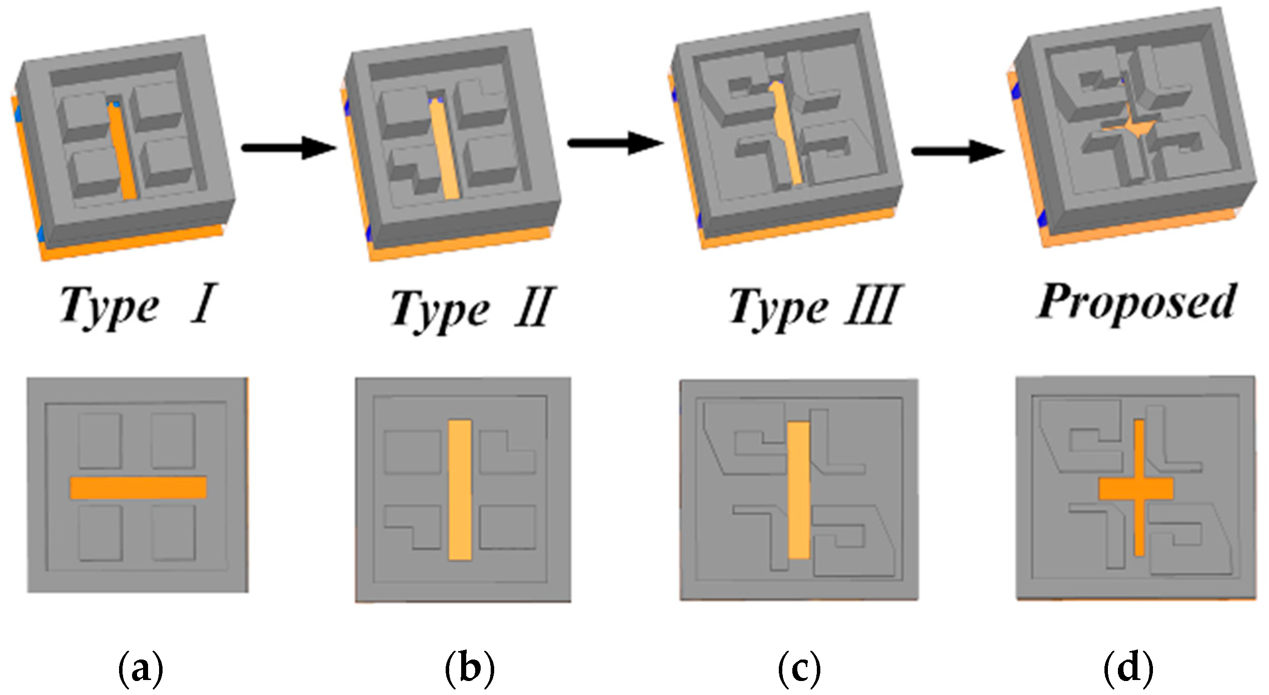
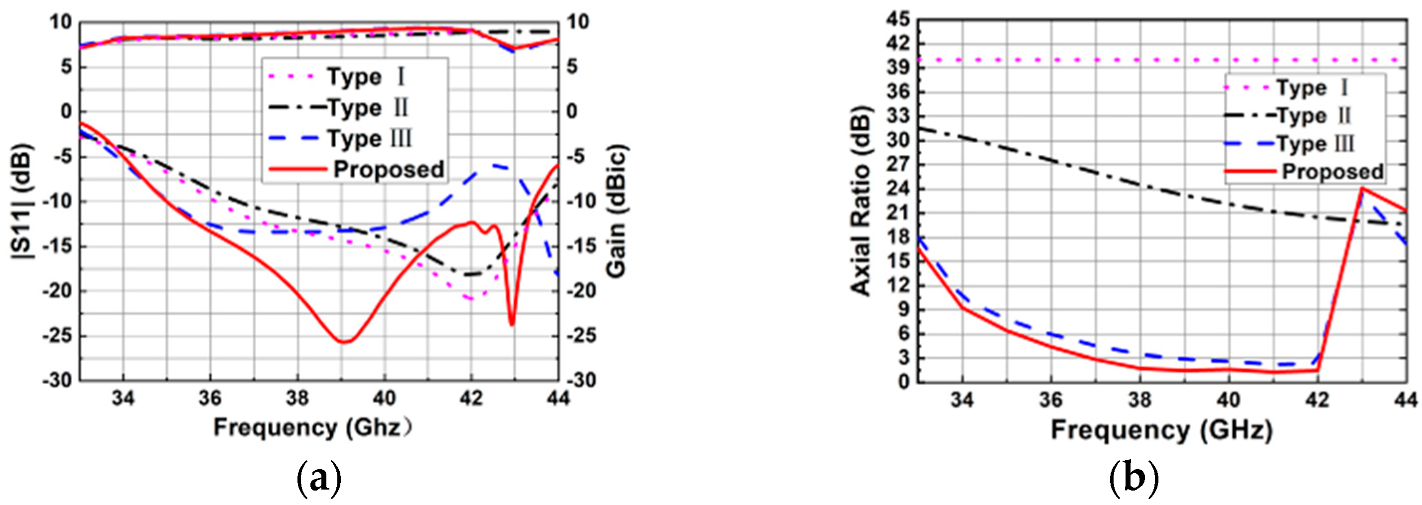
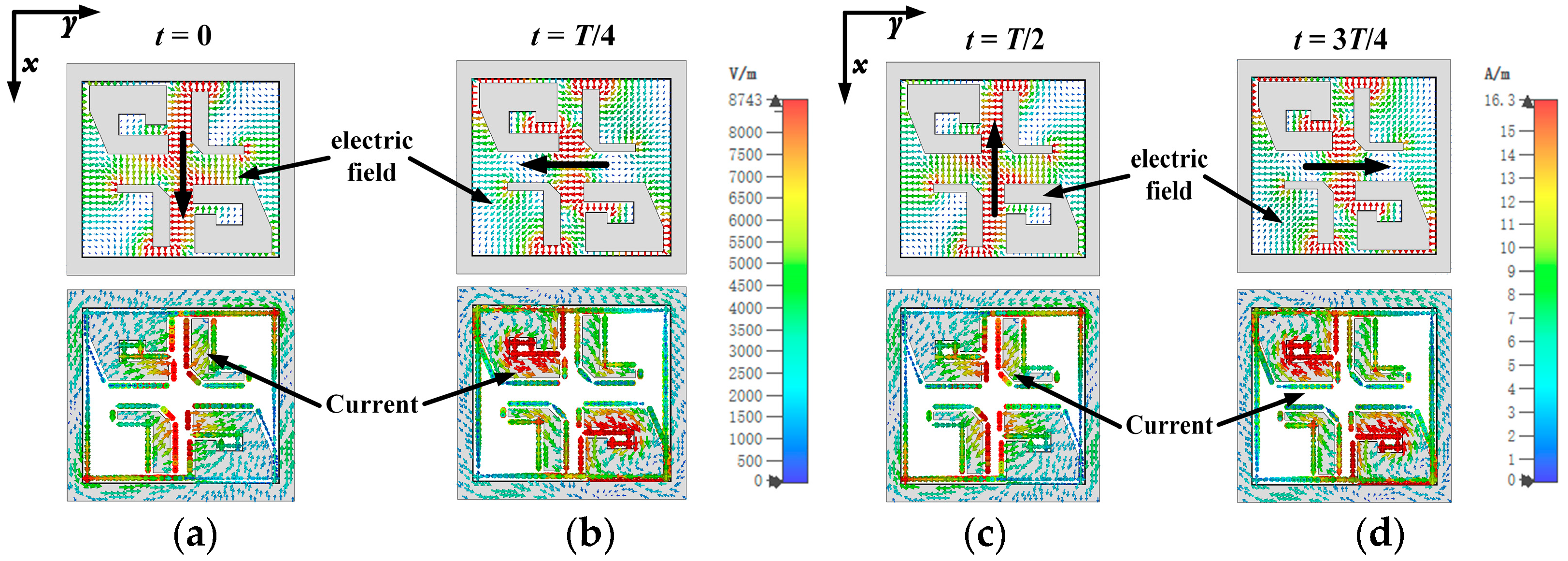
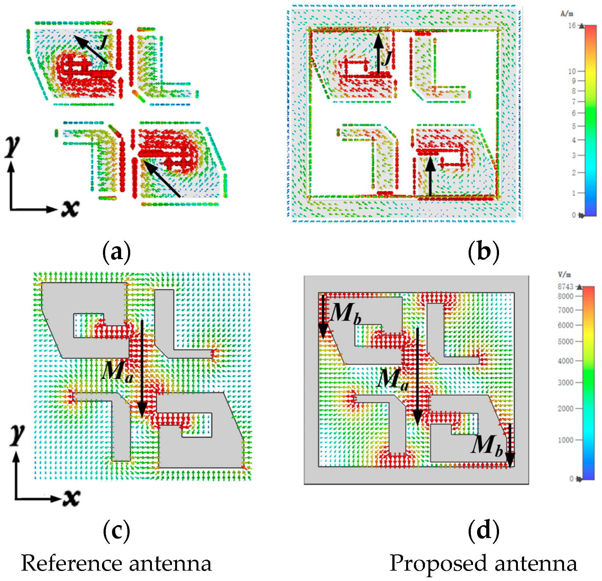
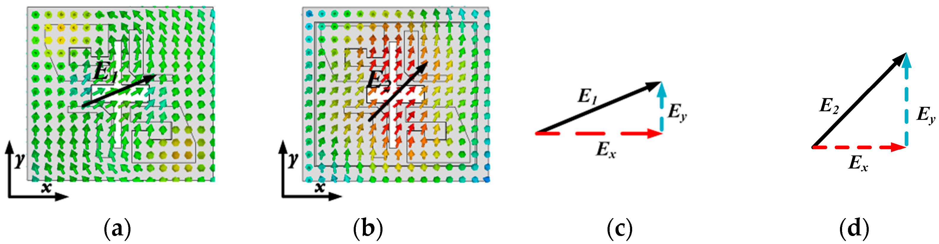
2.1.1. Analysis of the Proposed CP ME-Dipole

The design processes of the proposed CP ME-dipole antenna element are shown in Figure 2. In Figure 2a, a traditional LP ME-dipole antenna is designed. It consists of two pairs of metal posts, a metal cavity and corresponding SIW feeding structures. In order to enhance the perturbation, the posts have been modified as shown in Figure 2b. To further enhance the 3 dB AR bandwidth, the four metal posts are divided into two groups which are symmetrical in the center. One group of posts is cut into an L shape, while the other group of posts is cut into a ring shape as shown in Figure 2c. Its simulated 3 dB AR bandwidth is 7.9% from 38.8 to 42.0 GHz as shown in Figure 3b. In the final proposed design, the rectangular coupling slot is modified as a cross-shaped slot with two different lengths and widths which yields a 13.2% 3 dB AR bandwidth from 36.9 to 42.1 GHz. As shown in Figure 3a, it can be seen that the impedance matching has been significantly improved by introducing the cross-shaped coupling slot.
The simulated impedance bandwidth (|S11| ≤ −10 dB) of the proposed element is 21.4% from 35.0 to 43.4 GHz, while the simulated 3 dB AR bandwidth is 13.2% from 36.9 to 42.1 GHz. The simulated peak gain is 9.21 dBic at 40.5 GHz. The simulated results of the ME-dipole antenna element radiation patterns at 37 and 40 GHz are shown in Figure 4. The antenna element has stable gain, and the radiation patterns of the E-plane (yoz plane) and H-plane (xoz plane) are virtually equal.
To better explain the operating mechanism of the circular polarization, the electric field distributions at four states (t = 0, T/4, T/2, 3T/4, where T is a time period) are shown in Figure 5. The black arrow represents the direction of the E-field vector at the corresponding time period, which, over a time period rotates in a clockwise manner, so a left-hand CP (LHCP) wave can be generated. As shown in Figure 5a, at the time t = 0, the fields between the metal posts arranged along the y-axis and the metal posts’ surface current are minimized. At t = T/4, the fields on the gap between the metal posts and the cavity walls and metal posts’ surface current dominate, as illustrated in Figure 5b. So, the electric dipole mode and magnetic dipole mode are excited at time t = T/4. As shown in Figure 5d, at time t = 3T/4, the electric dipole and magnetic dipole are excited again with opposite field direction compared to the mode at t = T/4. Therefore, it can be concluded that the ME-dipole mode is excited.
To illustrate the function of the metal wall, a reference antenna element without a cavity is designed. The dimensions of all the structural parameters of the reference antenna are the same as the proposed CP antenna element, as shown in Figure 6a. Figure 6b,c show the comparisons of simulated |S11|, gain and AR results between the proposed CP antenna element and the reference antenna element. It can be seen that the presence of the cavity improves the impedance matching of the antenna and broadens the 3 db AR bandwidth. The antenna gain is enhanced in the frequency range from 33 to 42 GHz. Comparisons of simulated radiation patterns of the reference antenna element and proposed CP antenna element are shown in Figure 7. Compared with the radiation pattern of the proposed CP antenna element, the uniformity of the radiation patterns in E-plane and H-plane of the reference antenna element without a cavity deteriorates. The metal cavity in the proposed design introduces two magnetic dipoles (the gap between the metal post and the cavity) along the y-axis, which enhances the characteristics of the ME-dipole of the antenna, so as to improve the uniformity of the radiation pattern in E-plane and H-plane. It can be seen that the metal cavity also decreases the back lobe level.
In order to explain the significant improvement of antenna circular polarization performance caused by loading a metal cavity, the surface current distribution and electric field distribution of antenna elements with or without cavities were simulated, as shown in Figure 8. According to electromagnetic field theory, when the electric dipole current is parallel to the magnetic dipole current, the electric field of the electric dipole and the magnetic dipole is orthogonal, and the condition of generating circularly polarized wave is satisfied. After loading the metal cavity, the surface current on the metal posts is better aligned along the y-axis, as shown in Figure 8a,b. As shown in Figure 8b,d, this is parallel to the magnetic dipole current when the magnetic dipole is excited at t = T/4, proving that the circular polarization performance of the antenna is greatly improved through the perturbation of the metal cavity. As shown in Figure 8d, it can be noted that the metal cavity also introduces a pair of magnetic dipoles between the metal posts and the metal cavity, enhancing the ME-dipole characteristics of the antenna.
To delve deeper into the significant enhancement of the axial ratio (AR), we present the simulated electric field distributions of both the reference antenna and proposed antenna elements in Figure 9. According to the theory of electromagnetic fields, the generation of circularly polarized waves requires two linearly polarized components of constant amplitude and phase orthogonal. As depicted in Figure 9c,d, it is evident that upon loading the metallic cavity, there emerges an angular deviation between E1 and E2 at identical frequency points. This deviation predominantly stems from the reinforced electric field component along the y-axis subsequent to loading the metallic cavity. Consequently, through meticulous adjustments of the metallic posts, cross-slot, and metallic cavity dimensions, we can achieve two orthogonally linearly polarized components with a 90° phase difference at the cavity aperture.

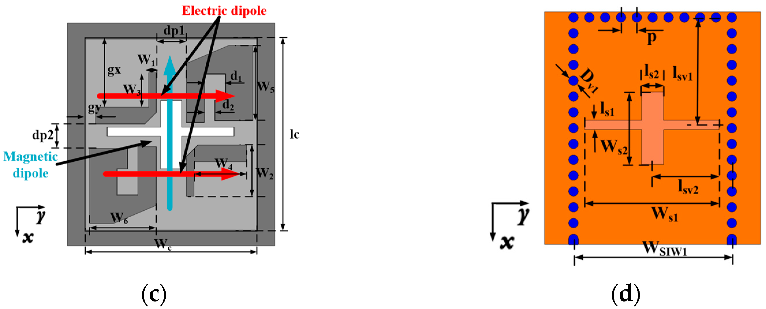
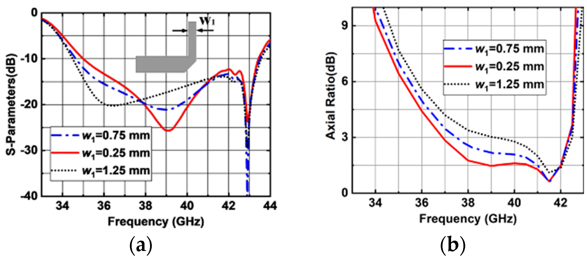
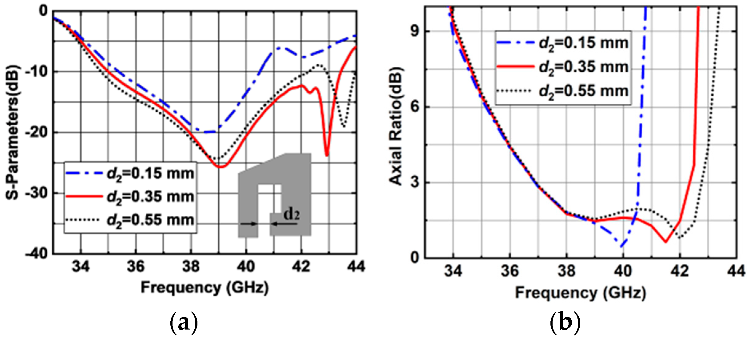
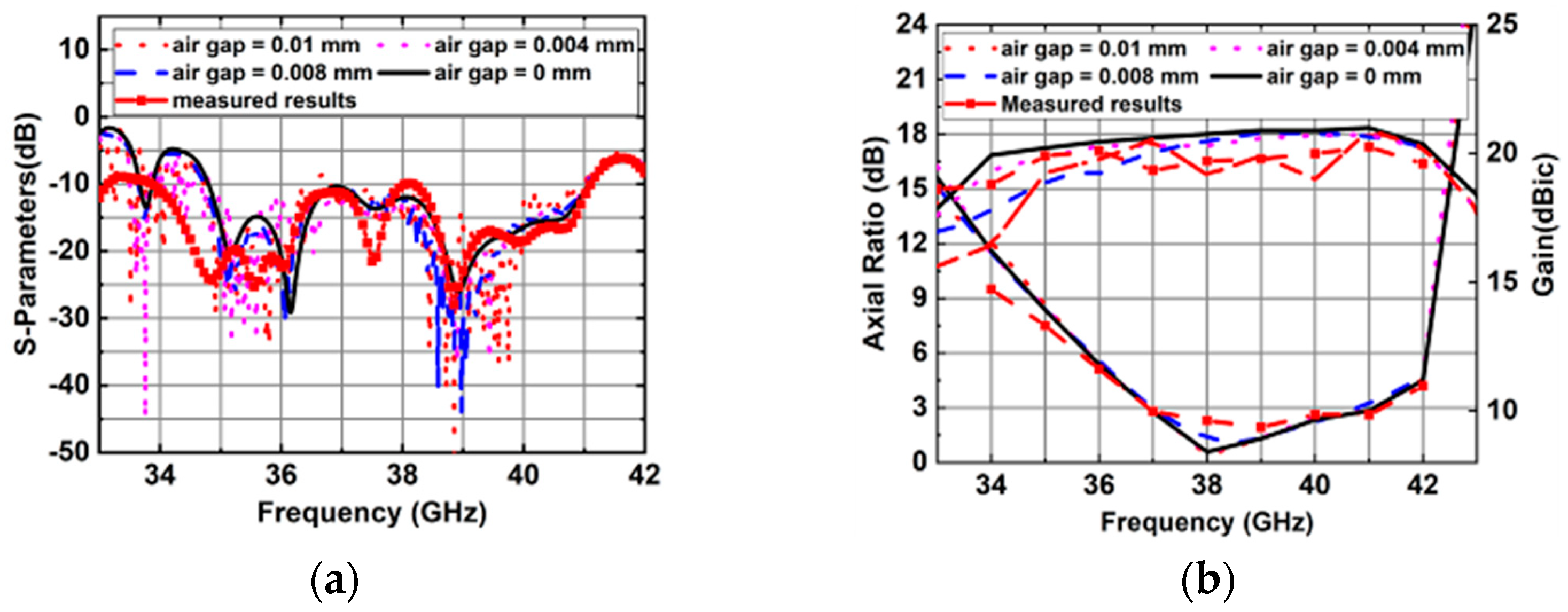
2.1.2. Parametric Studies

Studies of four important parameters, namely, Δh, w1, w5, and d2, were performed for the proposed CP antenna element. In this design, the height of the cavity is 2.4 mm, the height of the metal post is 2 mm, and the height difference between them is set as the variable Δh. Figure 10 shows the simulated results with different Δh. As Δh increases, the AR curves shift to a higher band, and the impedance matching is dramatically affected. Considering antenna matching and 3 db AR bandwidth, the optimized value of Δh is finally selected as 0.4 mm.
Figure 11 shows the simulated results with different lengths of L-shaped metal posts (w1). The lower resonant frequency point shifts to a lower band as w1 increases, while the higher resonant frequency point remains virtually unchanged. However, the 3 dB AR bandwidth at the lower band decreases. The final value of w1 is optimized to 0.25 mm.
The simulated |S11| and AR versus w5 are shown in Figure 12. When w5 varies, the impedance matching is slightly affected as shown in Figure 12a. The simulated results show that when w5 decreases, the AR performance deteriorates, as shown in Figure 12b. So, the optimized value of w5 is selected to be 2.48 mm. The simulated results show that upper and lower band AR could be optimized by the size of L-shaped and ring-shaped metal posts. It can be seen in Figure 13 that both the impedance matching, and AR performances are affected by the opening length of ring-shaped metal post (d2). As d2 increases from 0.15 to 0.55 mm, a wider 3 dB AR bandwidth can be achieved. However, the impedance matching deteriorates. Finally, the optimized value of d2 is selected to be 0.35 mm.

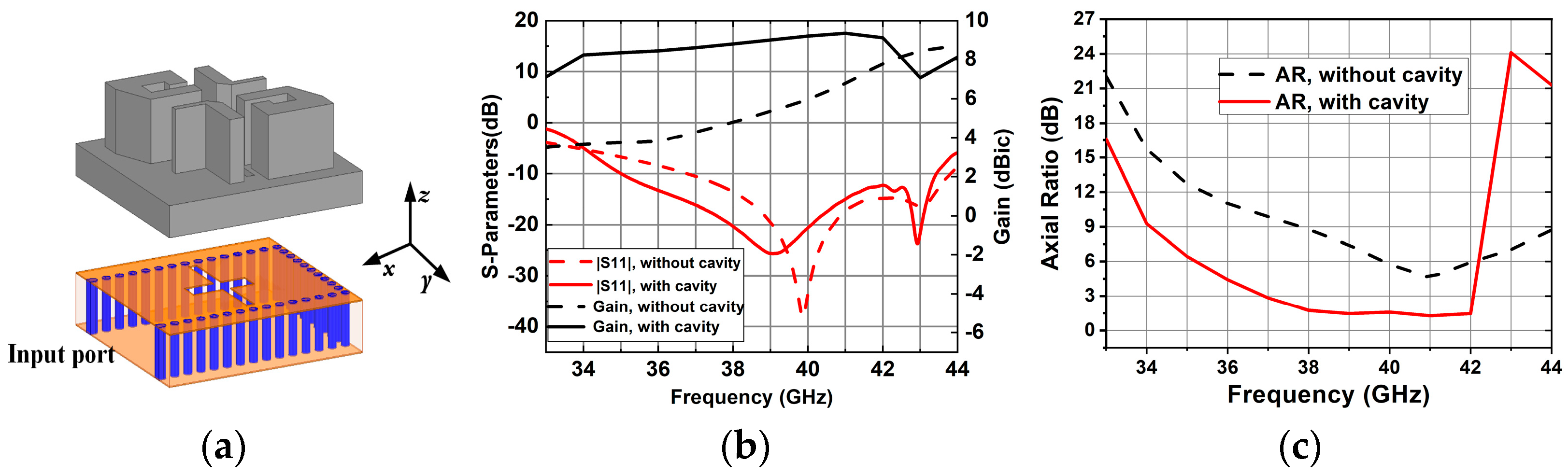
2.2. 4 × 4 Antenna Array Design

2.2.1. Design of the 2 × 2 CP ME-Dipole Antenna Subarray

Based on the proposed CP ME-dipole antenna element, a 2 × 2 CP antenna subarray was designed to obtain higher gain, as shown in Figure 14. In this subarray, a one-to-four wideband feeding network with two layers of 1.575 mm Rogers 5880 substrate is adopted. The energy is coupled from the rectangular slot on substrate 2 to four cross-shaped slots on substrate 1. The energy is equally distributed to the four coupling slots to excite four ME-dipole elements. By optimizing the double-layer four-port power divider, approximately equal power can be generated at the four output ports. The optimized dimensions of the 2 × 2 subarray are shown in Table 2. The simulated results for the 2 × 2 subarray are shown in Figure 15.

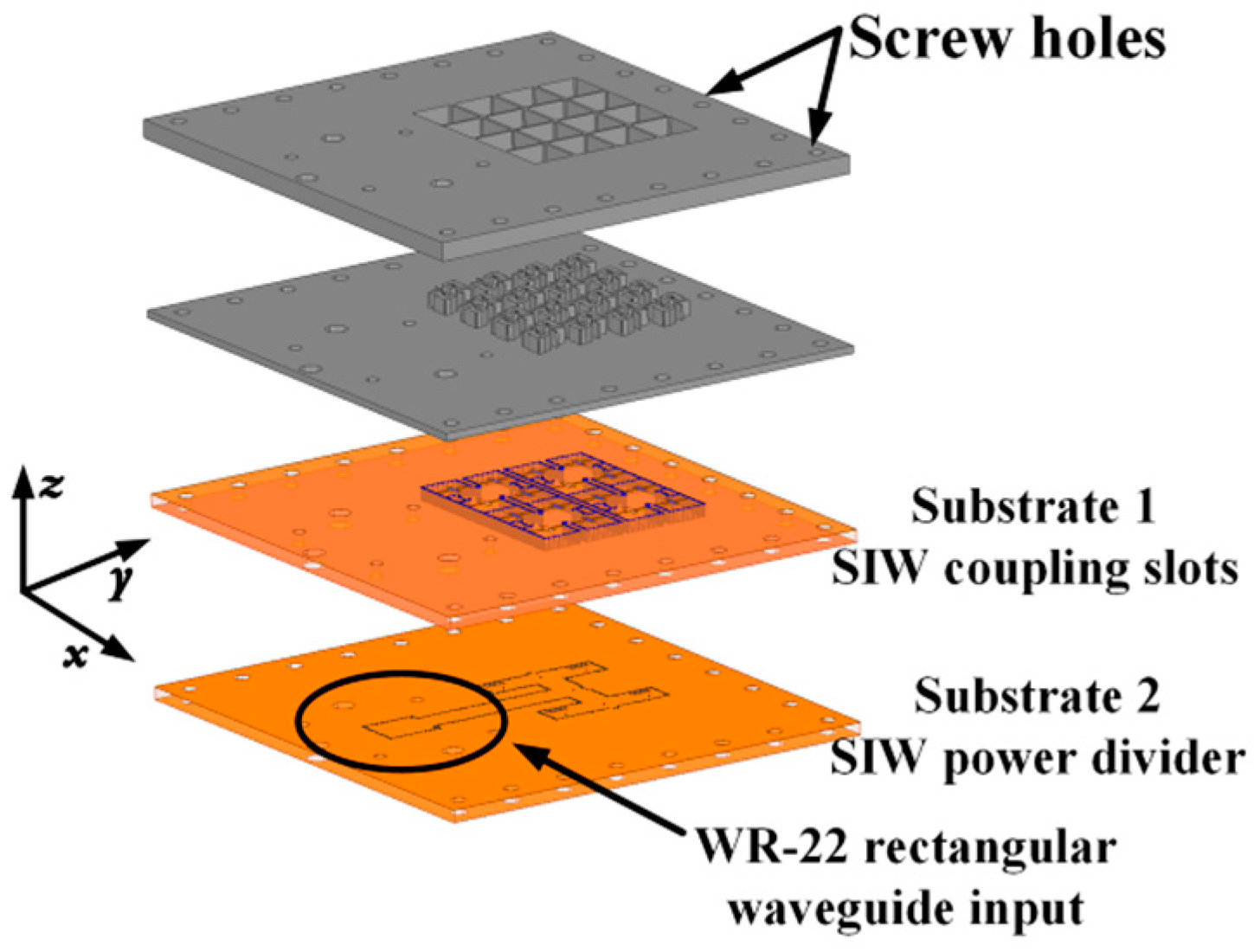
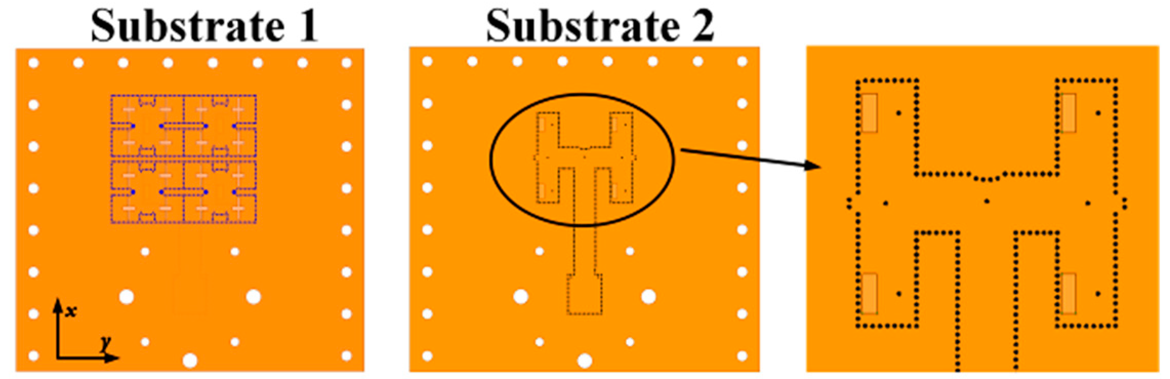
2.2.2. Design of the 4 × 4 Antenna Array

Based on the 2 × 2 CP antenna subarray described above, a 4 × 4 antenna array was designed, with its geometry shown in Figure 16. The feeding network of the 4 × 4 antenna array is shown in Figure 17. The entire antenna array is arranged vertically. Substrate 2 contains a one-to-four SIW power divider and a standard WR-22 rectangular waveguide to SIW transition.
In order to prove the beam scanning capability of the proposed antenna array, simulated results of 1 × 8 array and 4 × 4 array are given below. The beam scanning simulated performance of the 1 × 8 array at 38 and 41 GHz are shown in Figure 18a,b. At 38 and 41 GHz, the scan losses of 1 × 8 array are lower than 3.02 and 3.44 dBic, respectively. The 1 × 8 array can scan up to ±30°. The beam scanning simulated performance of the 4 × 4 array at 38 and 41 GHz are shown in Figure 18c,d. At 38 and 41 GHz, the scan losses of 4 × 4 array are lower than 2.33 and 2.39 dBic, respectively. The 4 × 4 array can scan up to ±25°. This proves that the proposed antenna array in this paper has relatively good beam scanning ability.

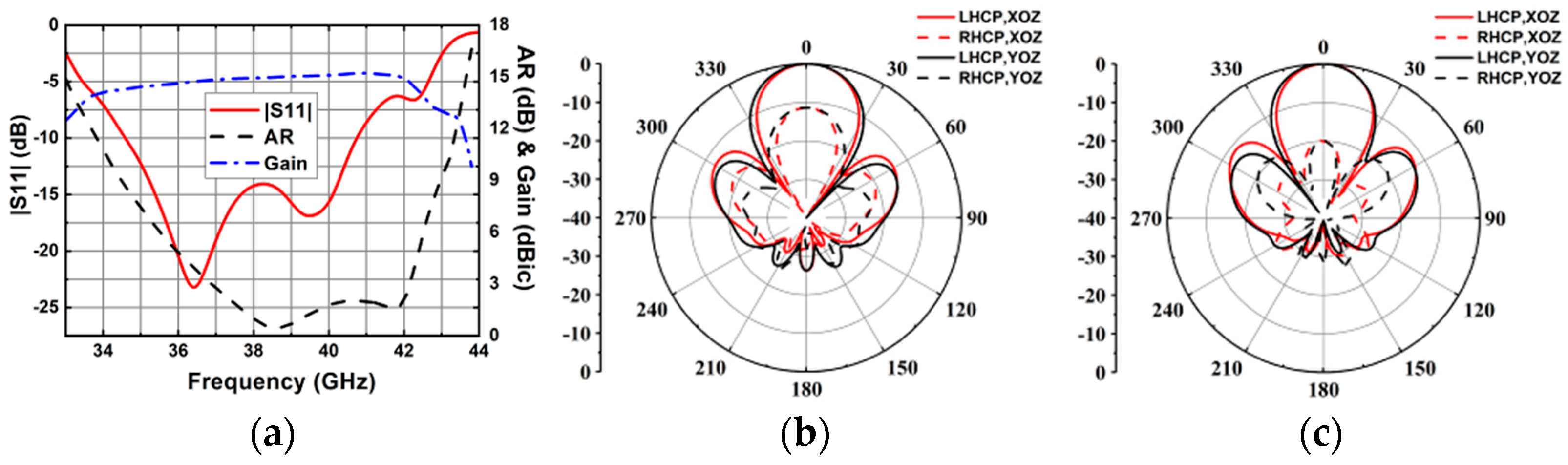
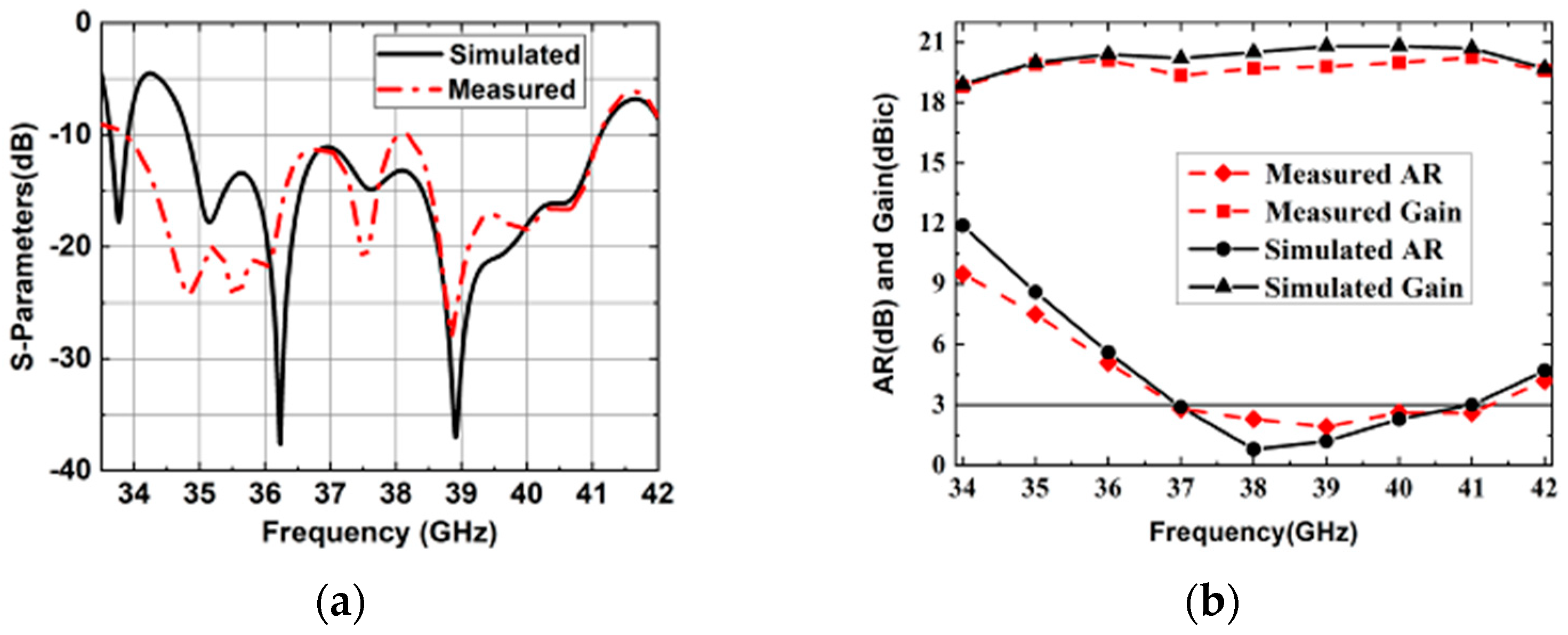
3. Experimental Results

The proposed 4 × 4 antenna array was fabricated using standard single-layer PCB technology, as shown in Figure 19. The screw holes were designed for assembly. The influences of the metal screws on the radiation performance of the array were included in the simulation. The overall dimensions of the antenna were 60.2 mm × 65.2 mm× 6.7 mm. Figure 20 shows the simulation and measurement results of this proposed 4 × 4 antenna array. It can be seen that the simulated and measured impedance matching the bandwidths of this antenna array are 16.8% (34.8–41.2 GHz) and 19.2% (33.9–41.1 GHz), respectively. The simulated and measured 3 db AR bandwidths are 10.3% (36.9–40.9 GHz) and 10.3% (37–41 GHz), respectively. The measured peak gain is 20.3 dBic at 41 GHz.
The measured radiation efficiency can be calculated by comparing the simulated directivity and measured gain. Then, the peak measured radiation efficiency of the 4 × 4 CP antenna array is 83.2% at 41 GHz. Figure 21 shows the simulated and measured radiation patterns of the 4 × 4 antenna array. It can be observed that the radiation patterns of the simulated and measured results are stable and consistent across the entire operating band. In the proposed CP antenna array, the aluminum plate and the two PCB substrates are fixed by screws; therefore, the effects of possible air gaps between substrate 1 and the aluminum plate should be considered. The simulated results of the 4 × 4 CP antenna array were considered. We took into account the possible air gaps between the PCB antenna array, with different air gap thicknesses are shown in Figure 22. Note that when the thickness of the air gaps reaches 0.008 and 0.01 mm, the impedance bandwidth deteriorates and the gains decrease at some frequencies, while the 3 db AR bandwidth remains largely unchanged. Also, the effect of the air gaps can be ignored when the thickness is 0.004 mm. This indicates that the possible air gaps can affect the performance of the assembled antenna array.

4. Discussion

Table 3 compares the proposed antenna array to previously reported CP MMW antenna arrays based on various parameters such as array configuration, thickness, impedance bandwidth, 3 db AR bandwidth and peak gain. Previous reports have highlighted that the majority of the 4 × 4 CP antenna arrays use microstrip radiating structures, resulting in peak gains less than 20 dBic. Thanks to the all-metal radiating structures, the proposed 4 × 4 antenna array obtains a high gain of 20.3 dBic. This work proposes a design method that can be utilized to develop a high-gain and low-cost MMW CP antenna array.

5. Conclusions

A high-gain SIW-fed MMW CP ME-dipole antenna array is proposed in this paper. A metal cavity is introduced to improve both the impedance and AR bandwidth, as well as to enhance the consistency of the E-plane and H-plane of the antenna. A 4 × 4 CP antenna array is designed, fabricated, and measured to validate the design concept. The measured results show that the CP antenna array achieves a wideband impedance bandwidth of 19.2%, a 3 db AR bandwidth of 10.3%, and a peak gain of 20.3 dBic. The measured results show that the antenna array has the advantages of high gain, high efficiency, etc. It demonstrates that the proposed high-gain CP antenna array is suitable for MMW communication.

Author Contributions

Conceptualization, J.X.; formal analysis, J.W. and Z.Y.; funding acquisition, C.H.; investigation, J.X.; methodology, J.X.; project administration, T.D. and Q.Y.; supervision, T.D. and Q.Y.; validation, C.H.; writing—original draft, J.W. and Z.Y.; writing—review and editing, J.W. All authors have read and agreed to the published version of the manuscript.

Funding

This work was supported by the Open Research Fund Program of the State Key Laboratory of Electromagnetic Information Control and Effects (grant no. SYS1W2024040311).

Data Availability Statement

Data are contained within the article.

Conflicts of Interest

The authors declare no conflict of interest.

Abbreviations

The following abbreviations are used in this manuscript:
CPCircularly polarized
ME-dipoleMagnetoelectric dipole
MMWMillimeter-wave
SIWSubstrate-integrated waveguide
LPLinearly polarized
LHCPLeft-hand circularly polarized
ARAxial ratio

References

  1. Deslandes, D.; Wu, K. Integrated microstrip and rectangular waveguide in planar form. IEEE Microw. Compom. Lett. 2001, 11, 68–70. [Google Scholar] [CrossRef]
  2. Li, Y.; Chen, Z.N.; Qing, X.; Zhang, Z.; Xu, J.; Feng, Z. Axial ratio bandwidth enhancement of 60-GHz substrate integrated waveguide-fed circularly polarized LTCC antenna array. IEEE Trans. Antennas Propag. 2012, 60, 4619–4626. [Google Scholar] [CrossRef]
  3. Wu, J.; Cheng, Y.J.; Fan, Y. Millimeter-wave wideband high-efficiency circularly polarized planar array antenna. IEEE Trans. Antennas Propag. 2016, 64, 535–542. [Google Scholar] [CrossRef]
  4. Liu, C.; Guo, Y.-X.; Bao, X.; Xiao, S.-Q. 60-GHz LTCC integrated circularly polarized helical antenna array. IEEE Trans. Antennas Propag. 2012, 60, 1329–1335. [Google Scholar] [CrossRef]
  5. Zhang, T.; Zhang, Y.; Cao, L.; Hong, W.; Wu, K. Single-layer wideband circularly polarized patch antennas for Q-Band applications. IEEE Trans. Antennas Propag. 2015, 63, 409–414. [Google Scholar] [CrossRef]
  6. Zhu, Q.; Ng, K.-B.; Chan, C.H. Printed circularly polarized spiral antenna array for millimeter-wave applications. IEEE Trans. Antennas Propag. 2017, 65, 636–643. [Google Scholar] [CrossRef]
  7. Zhang, L.; Wu, K.; Wong, S.W.; He, Y.; Chu, P.; Li, W.; Wang, K.X.; Gao, S. Wideband high-efficiency circularly polarized SIW-fed s-dipole array for millimeter-wave applications. IEEE Trans. Antennas Propag. 2020, 68, 2422–2427. [Google Scholar] [CrossRef]
  8. Zhang, Y.-X.; Jiao, Y.-C.; Zhang, L. Wideband circularly polarized array antennas with sequential-rotation polarization grid and simplified full-SIW feeding networks. IEEE Trans. Antennas Propag. 2020, 68, 6088–6097. [Google Scholar] [CrossRef]
  9. Zhu, C.; Xu, G.; Ding, D.; Wu, J.; Wang, W.; Huang, Z.X.; Wu, X.L. Low-profile wideband millimeter-wave circularly polarized antenna with hexagonal parasitic patches. IEEE Antennas Wirel. Propag. Lett. 2021, 20, 1651–1655. [Google Scholar] [CrossRef]
  10. Cheng, Y.; Dong, Y. Wideband circularly polarized planar antenna array for 5G millimeter-wave applications. IEEE Trans. Antennas Propag. 2021, 69, 2615–2627. [Google Scholar] [CrossRef]
  11. Sun, G.-H.; Wong, H. Circularly polarized elliptical cavity-backed patch antenna array for millimeter-wave applications. IEEE Trans. Antennas Propag. 2022, 70, 10512–10519. [Google Scholar] [CrossRef]
  12. Luk, K.M.; Wong, H. A new wideband unidirectional antenna element. Int. J. Microw. Opt. Technol. 2006, 1, 35–44. [Google Scholar]
  13. Gan, Z.; Tu, Z.-H.; Xie, Z.-M.; Chu, Q.-X.; Yao, Y. Compact wideband circularly polarized microstrip antenna array for 45 GHz application. IEEE Trans. Antennas Propag. 2018, 66, 6388–6392. [Google Scholar] [CrossRef]
  14. Cao, W.; Wang, Q.; Qian, Z.; Shi, S.; Jin, J.; Ding, K.; Zhang, B. Gain enhancement for wideband CP ME-dipole antenna by loading with spiral strip in Ku-band. IEEE Trans. Antennas Propag. 2018, 66, 962–966. [Google Scholar] [CrossRef]
  15. Xiang, L.; Wu, F.; Yu, C.; Jiang, Z.H.; Yao, Y.; Hong, W. A wideband circularly polarized magneto-electric dipole antenna array for millimeter-wave applications. IEEE Trans. Antennas Propag. 2022, 70, 3876–3881. [Google Scholar] [CrossRef]
  16. Ding, K.; Li, Y.; Wu, Y. Broadband circularly polarized magnetoelectric dipole antenna by loading parasitic loop. IEEE Trans. Antennas Propag. 2022, 70, 11085–11090. [Google Scholar] [CrossRef]
  17. Tan, Q.; Fan, K.; Yu, W.; Yu, Y.; Luo, G.Q. A broadband circularly polarized planar antenna array using magneto-electric dipole element with bent strips for Ka-band applications. IEEE Antennas Wirel. Propag. Lett. 2022, 22, 39–43. [Google Scholar] [CrossRef]
  18. Xu, J.; Hong, W.; Jiang, Z.H.; Zhang, H. Low-cost millimeter-wave circularly polarized planar integrated magneto-electric dipole and its arrays with low-profile feeding structures. IEEE Antennas Wirel. Propag. Lett. 2020, 19, 1400–1404. [Google Scholar] [CrossRef]
  19. Li, Y.; Luk, K.-M. A 60-GHz wideband circularly polarized aperture-coupled magneto-electric dipole antenna array. IEEE Trans. Antennas Propag. 2016, 64, 1325–1333. [Google Scholar] [CrossRef]
  20. Ji, Z.; Sun, G.-H.; Wong, H. A wideband circularly polarized complementary antenna for millimeter-wave applications. IEEE Trans. Antennas Propag. 2022, 70, 2392–2400. [Google Scholar] [CrossRef]
  21. Feng, B.; Lai, J.; Chung, K.L.; Chen, T.-Y.; Liu, Y.; Sim, C.-Y.-D. A compact wideband circularly polarized magneto-electric dipole antenna array for 5G millimeter-wave application. IEEE Trans. Antennas Propag. 2020, 68, 6838–6843. [Google Scholar] [CrossRef]
  22. Sun, F.; Li, Y.; Ge, L.; Wang, J. Millimeter-wave magneto-electric dipole antenna array with a self-supporting geometry for time-saving metallic 3-D printing. IEEE Trans. Antennas Propag. 2020, 68, 7822–7832. [Google Scholar] [CrossRef]
  23. Cao, J.; Wang, H.; Mou, S.; Soothar, P.; Zhou, J. An air cavity-fed circularly polarized magneto-electric dipole antenna array with gap waveguide technology for mm-wave applications. IEEE Trans. Antennas Propag. 2019, 67, 6211–6216. [Google Scholar] [CrossRef]
Figure 1. Geometry of the proposed CP antenna element. (a) 3D exploded view. (b) Side view. (c) Top view of the top aluminum plate. (d) Top view of the bottom substrate.
Sensors 25 03046 g001aSensors 25 03046 g001b
Figure 2. Design process of the proposed CP ME-dipole antenna element. (a) Type I: traditional LP ME-dipole. (b) Type II: introduce a suitable perturbation (c) Type III: introduce ring-shaped metal posts. (d) Proposed CP antenna element.
Sensors 25 03046 g002
Figure 3. Performance comparisons of the three types of antenna elements. (a) Simulated |S11| and gains. (b) Simulated ARs.
Sensors 25 03046 g003
Figure 4. Simulated radiation patterns of the antenna element at (a) 37 GHz and (b) 40 GHz.
Sensors 25 03046 g004
Figure 5. Simulated electric field and current distributions of the proposed antenna element at 39 GHz over a period of time. (a) t = 0. (b) t = T/4. (c) t = T/2. (d) t = 3T/4.
Sensors 25 03046 g005
Figure 6. Geometry of the reference antenna element without a cavity. (a) 3D view. (b) Simulated |S11| and gains with and without cavity. (c) Simulated ARs with and without cavity.
Sensors 25 03046 g006
Figure 7. Comparisons of the simulated radiation patterns at 41 GHz. (a) the reference antenna element, (b) the proposed CP antenna element.
Sensors 25 03046 g007
Figure 8. Surface current and electric field distribution between the reference antenna and the proposed antenna at 38 GHz. (a,b) Current distribution at t = 0. (c,d) Electric field distribution at t = T/4.
Sensors 25 03046 g008
Figure 9. Simulated E-field distributions with the same phase at 38 GHz. (a) E-field distribution of the reference antenna. (b) E-field distribution of the proposed antenna. (c) Qualitative analysis of the E-field relationship of the reference antenna. (d) Qualitative analysis of the E-field relationship of the proposed antenna.
Sensors 25 03046 g009
Figure 10. Simulated results of the proposed antenna element with different Δh values. (a) |S11|. (b) ARs.
Sensors 25 03046 g010
Figure 11. Simulated results of the proposed antenna element with different w1 values. (a) |S11|. (b) ARs.
Sensors 25 03046 g011
Figure 12. Simulated results of the proposed antenna element with different w5 values. (a) |S11|. (b) ARs.
Sensors 25 03046 g012
Figure 13. Simulated results of the proposed antenna element with different d2 values. (a) |S11|. (b) ARs.
Sensors 25 03046 g013
Figure 14. Geometry of the proposed 2 × 2 antenna subarray. (a) 3D exploded view. (b) Top view. (c) Substrate 1. (d) Substrate 2.
Sensors 25 03046 g014
Figure 15. Simulated results of the 2 × 2 CP ME-dipole antenna subarray. (a) |S11|, gain, and AR. (b) Radiation pattern at 36 GHz. (c) Radiation pattern at 40 GHz.
Sensors 25 03046 g015
Figure 16. Geometry of the 4 × 4 CP antenna array.
Sensors 25 03046 g016
Figure 17. Geometric configurations of two-layer dielectric substrates.
Sensors 25 03046 g017
Figure 18. Radiation patterns of the yoz-plane of the proposed antenna array at various scanning angles. (a) 1 × 8 array at 38 GHz. (b) 1 × 8 array at 41 GHz. (c) 4 × 4 array at 38 GHz. (d) 4 × 4 array at 41 GHz.
Sensors 25 03046 g018
Figure 19. Fabricated 4 × 4 CP antenna array. (a) Disassembled drawing. (b) Assembly drawing of the prototype.
Sensors 25 03046 g019
Figure 20. Simulated and measured results of the 4 × 4 CP antenna array. (a) |S11|. (b) ARs and gain.
Sensors 25 03046 g020
Figure 21. Simulated and measured radiation patterns of the 4 × 4 CP antenna array at (a) 37 GHz, (b) 39 GHz, and (c) 41 GHz.
Sensors 25 03046 g021
Figure 22. Simulated and measured results of the 4 × 4 CP antenna array with different thicknesses of the air gaps. (a) |S11|. (b) ARs and gain.
Sensors 25 03046 g022
Table 1. Dimensions of the proposed antenna element (unit: mm).
Parametersw1w2w3w4w5w6ws1ws2wsiw1
Values0.251.71.151.752.482.24.252.35
Parameterswcls1ls2lsv1lsv2lchwhghp
Values5.70.30.73.42.56.42.412
ParametersΔhd1d2dp1dp2gxgyDv1p
Values0.40.70.350.30.810.352.30.30.5
Table 2. Dimensions of the proposed 2 × 2 antenna subarray (unit: mm).
Parametersd3d4d5d6duyduxDv2ws3wsv3
Values0.454.152.81.436.156.820.82.72.2
Parameterswsiw2ls3lsv3lm
Values410.81.2
Table 3. Comparisons of MMW antenna arrays.
Ref.No. of ElementThickness (λ0)f0 (GHz)TypeFeeding NetworkImp.
BW %
3 db AR
BW %
Radiation Efficiency %Peak
Gain (dBic)
[3]4 × 40.2128.35Slot Microstrip line28.614>6518.2
[4]4 × 40.4060Helical Microstrip line2220n.a.15.2
[6]4 × 4n.a.60SpiralSIW14.121.187.119.5
[9]4 × 40.3030.5Parasitic patchesSIW27.728.5n.a.17.85
[13]4 × 40.1545ME-dipoleMicrostrip line>24.416n.a.18.8
[18]4 × 40.0228.63ME-dipoleMicrostrip line21.835.9n.a.18.3
[22] *8 × 82.2031.5ME-dipoleAir-filled waveguide32.4n.a.7227.1
[23]4 × 82.1990ME-dipoleGWG16.517n.a.23
This work4 × 40.8437.5ME-dipoleSIW19.210.383.220.3
λ0: free-space wavelength at center frequency. *: linearly polarized antenna array.
Disclaimer/Publisher’s Note: The statements, opinions and data contained in all publications are solely those of the individual author(s) and contributor(s) and not of MDPI and/or the editor(s). MDPI and/or the editor(s) disclaim responsibility for any injury to people or property resulting from any ideas, methods, instructions or products referred to in the content.

