
Flare: An FPGA-Based Full Precision Low Power CNN Accelerator with Reconfigurable Structure


Abstract
1. Introduction
- We introduce a design space exploration (DSE) model aimed at evaluating various accelerator configuration parameters accurately, including resource consumption and processing latency. This model enables us to significantly reduce the development period by providing precise performance estimations across multiple criteria.
- We propose a vector dot product with variable length to unify the computation pattern of convolutional and fully connected layers in CNNs. The fine-grained length, in conjunction with DSE, facilitates a balanced allocation of computational resources and off-chip memory bandwidth.
- We adopt a run-time reconfiguration method to maximize each layer’s access to computational resources. The extra time overhead introduced by reconfiguration flows can be offset by faster processing time, thereby reducing overall inference latency.
2. Related Works
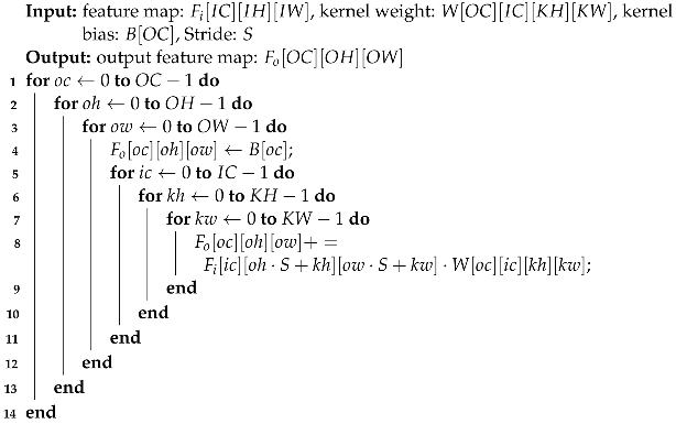
| Algorithm 1: Nested Loop Implementation for Convolutional Layer |
 |
3. Design Space Exploration
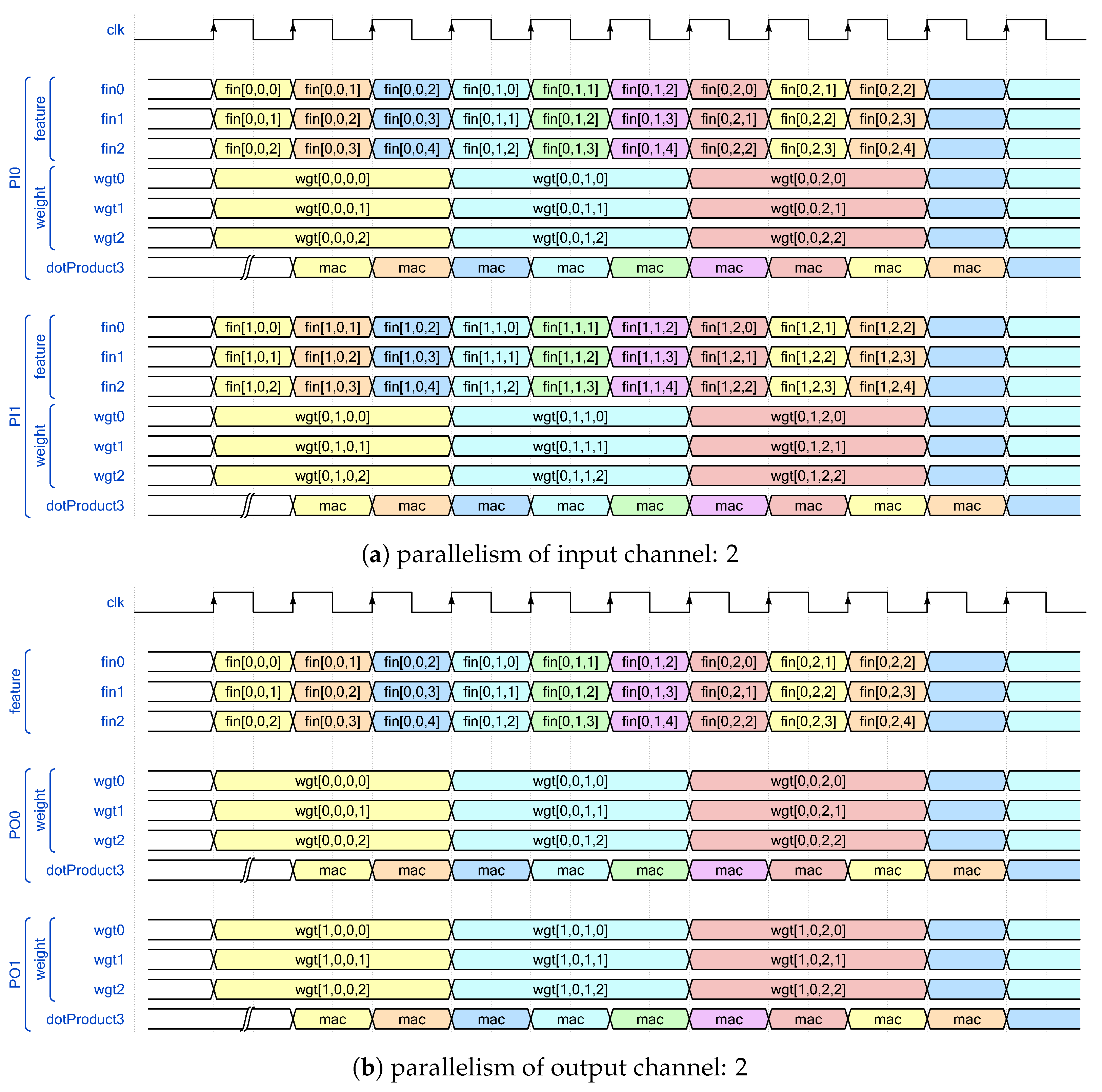
3.1. Dot Product with Variable Length
3.2. Bandwidth-Aware Parallelism Allocation Scheme
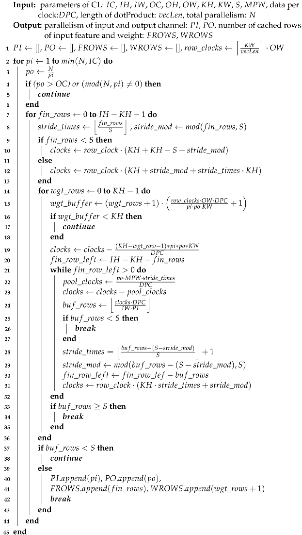
| Algorithm 2: Parallelism Allocation Algorithm |
 |
3.3. Decision of the Best Design Point
| Algorithm 3: Overall flow of the proposed DSE algorithm |
 |
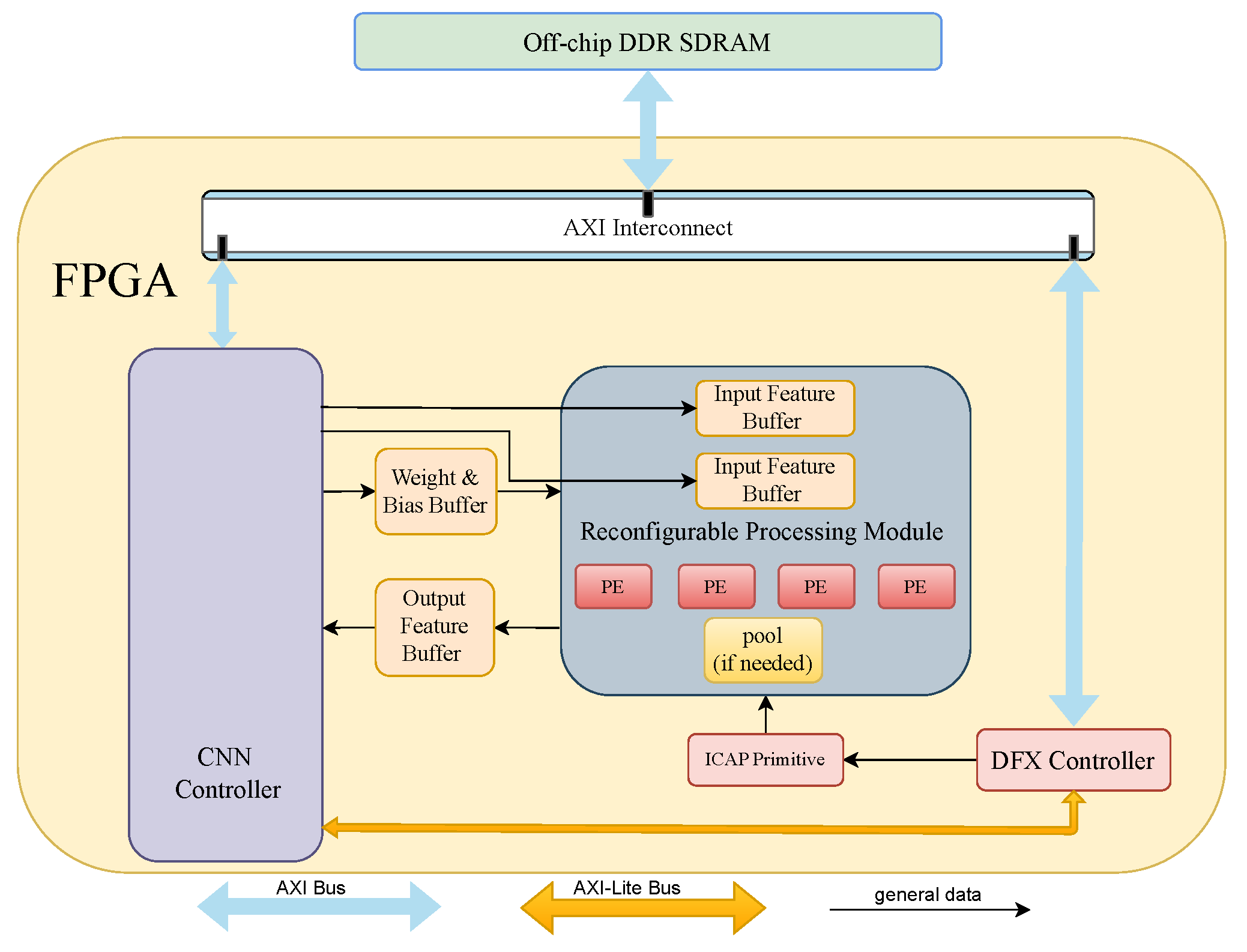
4. Architecture of Proposed CNN Accelerator
4.1. Integration with Design Space Exploration
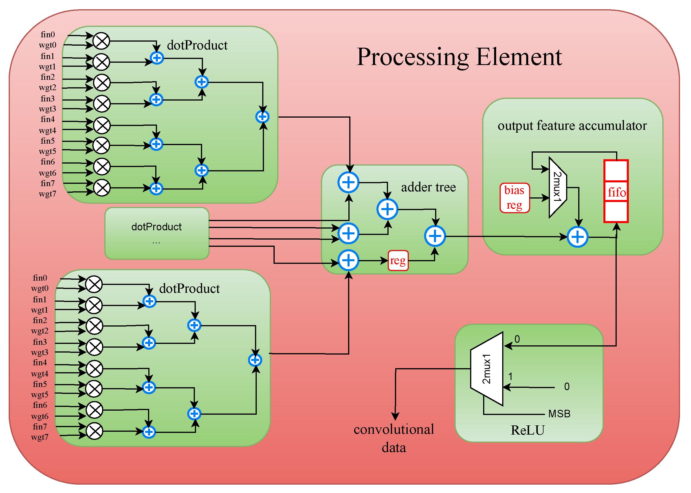
4.2. Processing Element
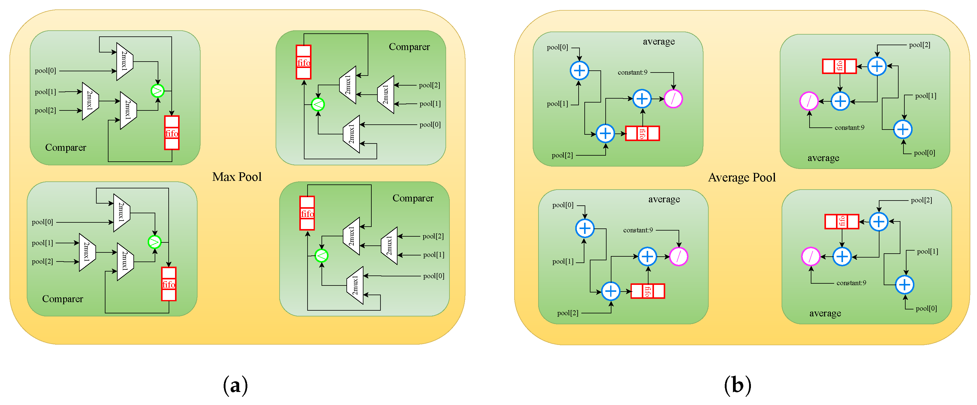
4.3. Pooling Layer
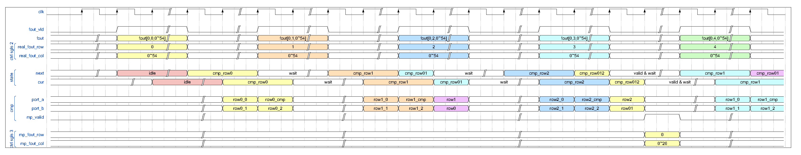
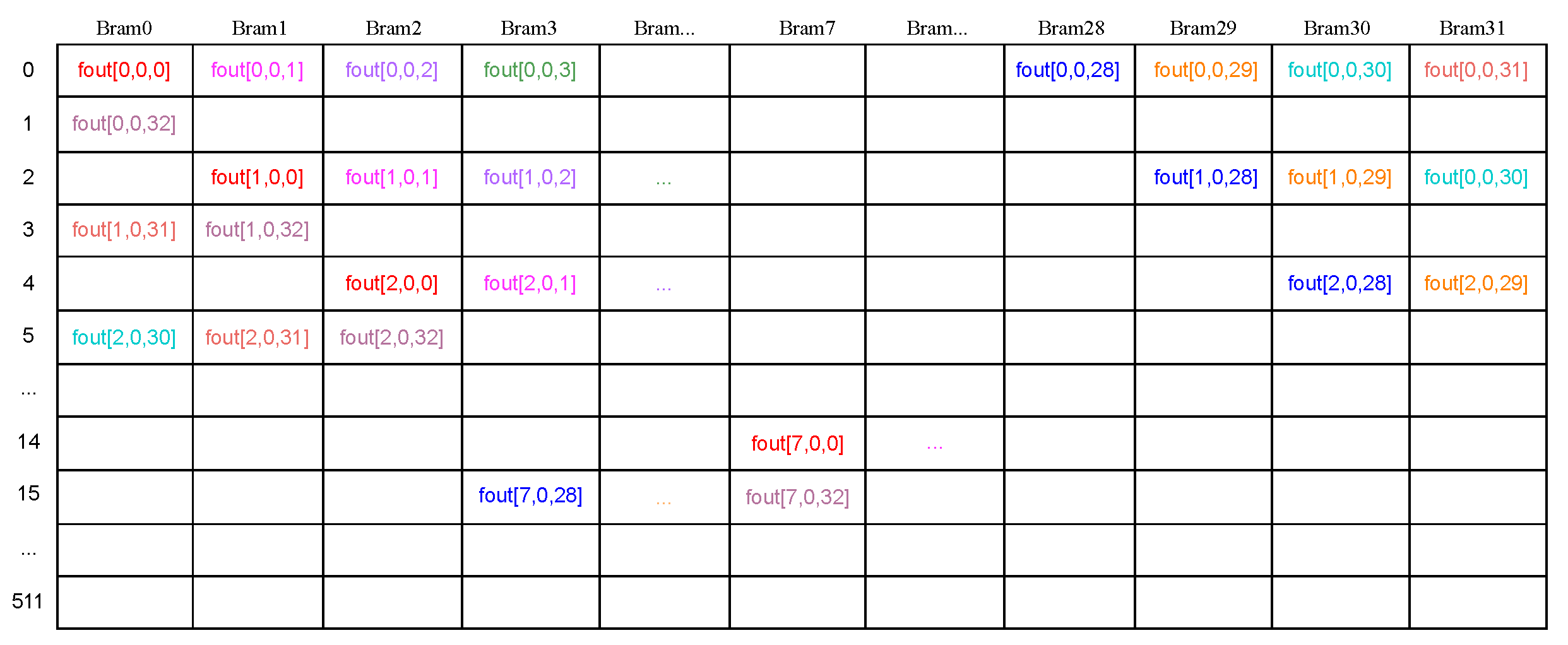
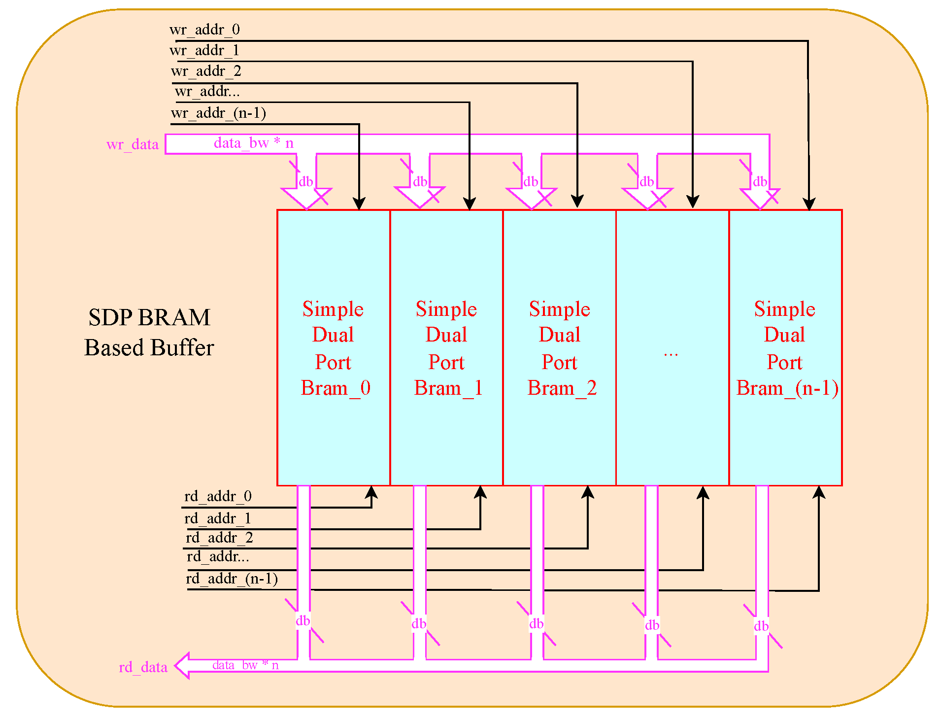
4.4. Data Buffer
5. Experimental Results
5.1. Results of Design Space Exploration
5.2. Resource Consumption and Latency in FPGA Implementations
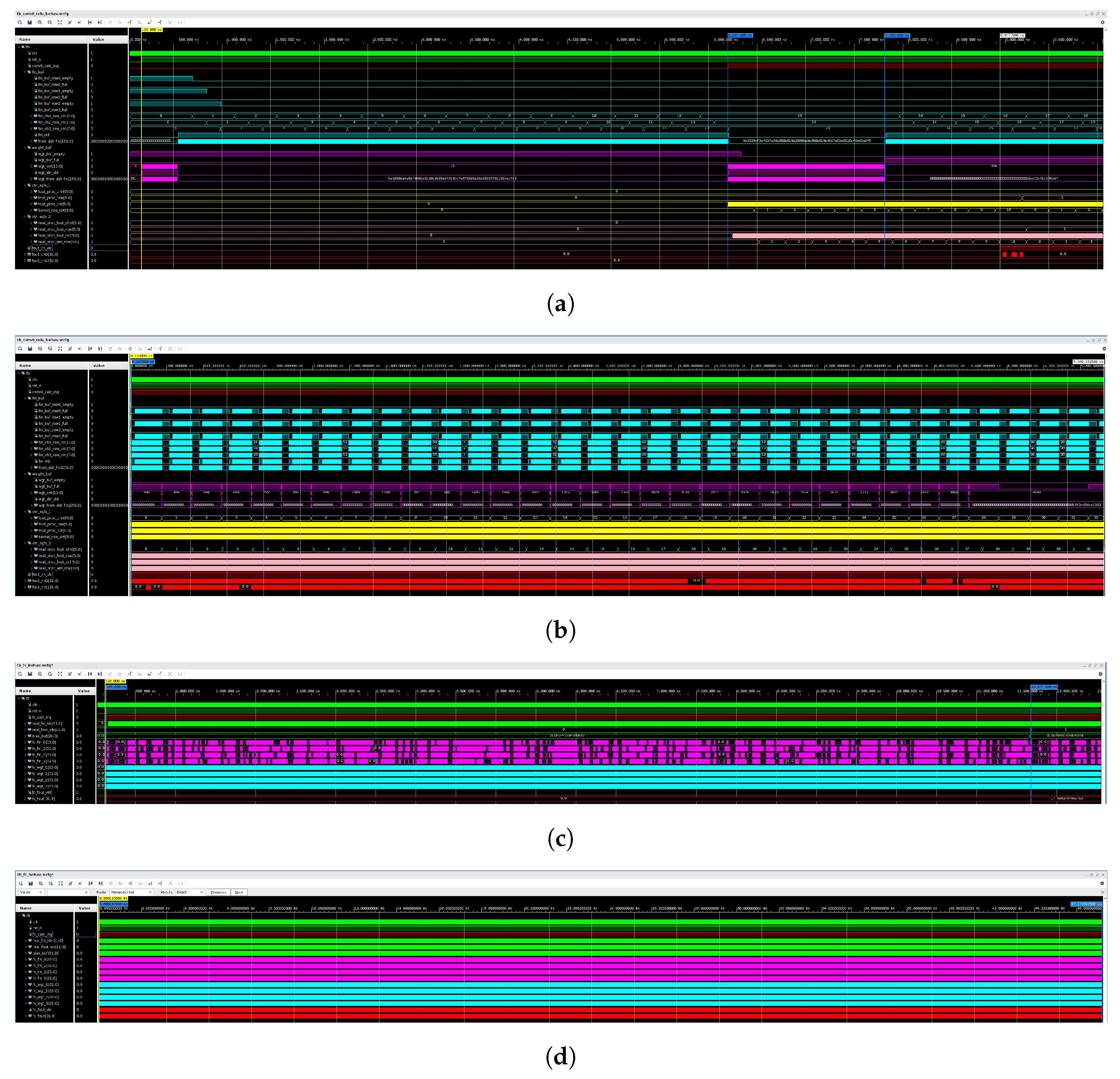
5.3. Simulation as Case Study
5.4. Compare with Previous Works
6. Conclusions
Author Contributions
Funding
Institutional Review Board Statement
Informed Consent Statement
Data Availability Statement
Conflicts of Interest
Abbreviations
| CNN | Convolutional Neural Network |
| FPGA | Filed Programmable Gate Array |
| MAC | Multiply ACcumulate |
| ASIC | Application Specific Integrated Circuit |
| HLS | High Level Synthesis |
| DSE | Design Space Exploration |
| CL | Convolutional Layer |
| FCL | Fully Connected Layer |
| GEMM | General Matrix Multiplication |
| FFT | Fast Fourier Transform |
| PE | Processing Element |
| PI | Parallelism levels of Input channel |
| PO | Parallelism levels of Output channel |
| DPC | Data Per Clock |
References
- LeCun, Y.; Bottou, L.; Bengio, Y.; Haffner, P. Gradient-based Learning Applied to Document Recognition. Proc. IEEE 2008, 86, 2278–2324. [Google Scholar] [CrossRef]
- Rehman, A.; Khan, M.A.; Saba, T.; Mehmood, Z.; Tariq, U.; Ayesha, N. Microscopic Brain Tumor Detection and Classification Using 3D CNN and Feature Selection Architecture. Microsc. Res. Tech. 2021, 84, 133–149. [Google Scholar] [CrossRef]
- Li, P.; Chen, X.; Shen, S. Stereo R-cnn Based 3d Object Detection for Autonomous Driving. In Proceedings of the IEEE/CVF Conference on Computer Vision and Pattern Recognition, Los Angeles, CA, USA, 16–20 June 2019; pp. 7644–7652. [Google Scholar]
- Alzubaidi, L.; Zhang, J.; Humaidi, A.J.; Al-Dujaili, A.; Duan, Y.; Al-Shamma, O.; Santamaría, J.; Fadhel, M.A.; Al-Amidie, M.; Farhan, L. Review of Deep Learning: Concepts, CNN Architectures, Challenges, Applications, Future Directions. J. Big Data 2021, 8, 1–74. [Google Scholar] [CrossRef] [PubMed]
- Hu, Y.; Liu, Y.; Liu, Z. A Survey on Convolutional Neural Network Accelerators: GPU, FPGA and ASIC. In Proceedings of the 2022 14th International Conference on Computer Research and Development (ICCRD), Shenzhen, China, 7–9 January 2022; pp. 100–107. [Google Scholar]
- Zhang, C.; Li, P.; Sun, G.; Guan, Y.; Xiao, B.; Cong, J. Optimizing Fpga-based Accelerator Design for Deep Convolutional Neural Networks. In Proceedings of the 2015 ACM/SIGDA International Symposium on Field-Programmable Gate Arrays, Monterey, CA, USA, 22–24 February 2015; pp. 161–170. [Google Scholar]
- Madineni, M.C.; Vega, M.; Yang, X. Parameterizable Design on Convolutional Neural Networks Using Chisel Hardware Construction Language. Micromachines 2023, 14, 531. [Google Scholar] [CrossRef] [PubMed]
- Williams, S.; Waterman, A.; Patterson, D. Roofline: An Insightful Visual Performance Model for Multicore Architectures. Commun. ACM 2009, 52, 65–76. [Google Scholar] [CrossRef]
- Sun, M.; Zhao, P.; Gungor, M.; Pedram, M.; Leeser, M.; Lin, X. 3D CNN Acceleration on FPGA Using Hardware-aware Pruning. In Proceedings of the 2020 57th ACM/IEEE Design Automation Conference (DAC), Francisco, CA, USA, 20–24 July 2020; pp. 1–6. [Google Scholar]
- Courbariaux, M.; Bengio, Y.; David, J.-P. Binaryconnect: Training Deep Neural Networks with Binary Weights During Propagations. In Proceedings of the 28th International Conference on Neural Information Processing Systems, Montreal, Canada, 7–12 December 2015; pp. 3123–3131. [Google Scholar]
- Zhu, C.; Han, S.; Mao, H.; Dally, W.J. Trained ternary quantization. arXiv 2016, arXiv:1612.01064. [Google Scholar]
- Jacob, B.; Kligys, S.; Chen, B.; Zhu, M.; Tang, M.; Howard, A.; Adam, H.; Kalenichenko, D. Quantization and Training of Neural Networks for Efficient Integer-arithmetic-only Inference. In Proceedings of the IEEE Conference on Computer Vision and Pattern Recognition, Salt Lake City, UT, USA, 18–23 June 2018; pp. 2704–2713. [Google Scholar]
- Gupta, S.; Agrawal, A.; Gopalakrishnan, K.; Narayanan, P. Deep Learning with Limited Numerical Precision. In Proceedings of the International Conference on Machine Learning, Lille, France, 6–11 July 2015; pp. 1737–1746. [Google Scholar]
- Bengio, Y.; Léonard, N.; Courville, A. Estimating or propagating gradients through stochastic neurons for conditional computation. arXiv 2013, arXiv:1308.3432. [Google Scholar]
- Zhang, W.; Jiang, M.; Luo, G. Evaluating Low-memory Gemms for Convolutional Neural Network Inference on FPGAS. In Proceedings of the 2020 IEEE 28th Annual International Symposium on Field-Programmable Custom Computing Machines (FCCM), Fayetteville, AR, USA, 3–6 May 2020; pp. 28–32. [Google Scholar]
- Liang, Y.; Lu, L.; Xiao, Q.; Yan, S. Evaluating Fast Algorithms for Convolutional Neural Networks on Fpgas. IEEE Trans. Comput. -Aided Des. Integr. Circuits Syst. 2019, 39, 857–870. [Google Scholar] [CrossRef]
- Liu, S.; Fan, H.; Luk, W. Design of Fully Spectral Cnns for Efficient Fpga-based Acceleration. IEEE Trans. Neural Netw. Learn. Syst. 2022, 1–13. [Google Scholar] [CrossRef] [PubMed]
- Jun, H.; Ye, H.; Jeong, H.; Chen, D. Autoscaledse: A Scalable Design Space Exploration Engine for High-level Synthesis. ACM Trans. Reconfigurable Technol. Syst. 2023, 16, 1–30. [Google Scholar] [CrossRef]
- Huang, W.; Wu, H.; Chen, Q.; Luo, C.; Zeng, S.; Li, T.; Huang, Y. Fpga-based High-throughput CNN Hardware Accelerator with High Computing Resource Utilization Ratio. IEEE Trans. Neural Netw. Learn. Syst. 2021, 33, 4069–4083. [Google Scholar] [CrossRef] [PubMed]
- Zhang, C.; Sun, G.; Fang, Z.; Zhou, P.; Pan, P.; Cong, J. Caffeine: Toward Uniformed Representation and Acceleration for Deep Convolutional Neural Networks. IEEE Trans. Comput.-Aided Des. Integr. Circuits Syst. 2019, 38, 2072–2085. [Google Scholar] [CrossRef]
- Nguyen, D.; Kim, D.; Lee, J. Double MAC: Doubling the Performance of Convolutional Neural Networks on Modern Fpgas. In Proceedings of the Design, Automation & Test in Europe Conference & Exhibition (DATE), Lausanne, Switzerland, 27–31 March 2017; pp. 890–893. [Google Scholar]
- Ma, Y.; Cao, Y.; Vrudhula, S.; Seo, J. Optimizing the Convolution Operation to Accelerate Deep Neural Networks on FPGA. IEEE Trans. Very Large Scale Integr. VLSI Syst. 2018, 26, 1354–1367. [Google Scholar] [CrossRef]
- Chen, J.; Liu, L.; Liu, Y.; Zeng, X. A Learning Framework for N-bit Quantized Neural Networks Toward Fpgas. IEEE Trans. Neural Netw. Learn. Syst. 2020, 32, 1067–1081. [Google Scholar] [CrossRef] [PubMed]
- Krizhevsky, A.; Sutskever, I.; Hinton, G.E. Imagenet Classification with Deep Convolutional Neural Networks. Adv. Neural Inf. Process. Syst. 2012, 25, 1–9. [Google Scholar] [CrossRef]
- Simonyan, K.; Zisserman, A. Very deep convolutional networks for large-scale image recognition. arXiv 2014, arXiv:1409.1556. [Google Scholar]
- Qu, X.; Huang, Z.; Xu, Y.; Mao, N.; Cai, G.; Fang, Z. Cheetah: An Accurate Assessment Mechanism and a High-throughput Acceleration Architecture Oriented toward Resource Efficiency. IEEE Trans. Comput.-Aided Des. Integr. Circuits Syst. 2020, 40, 878–891. [Google Scholar] [CrossRef]
- Qiu, J.; Wang, J.; Yao, S. Going Deeper with Embedded FPGA Platform for Convolutional Neural Network. In Proceedings of the 2016 ACM/SIGDA International Symposium on Field-Programmable Gate Arrays, Monterey, CA, USA, 21–23 February 2016; pp. 26–35. [Google Scholar]
- Bajaj, R.; Fahmy, S. Multi-pumping Flexible DSP Blocks for Resource Reduction on Xilinx Fpgas. IEEE Trans. Comput.-Aided Des. Integr. Circuits Syst. 2017, 36, 1471–1482. [Google Scholar]


| Operator | XC7A100T | ZU15EG | ||||||
|---|---|---|---|---|---|---|---|---|
| LUT | FF | DSP | Latency | LUT | FF | DSP | Latency | |
| adder | 322 | 135 | 1 | 1 | 279 | 135 | 2 | 1 |
| mul | 277 | 135 | 1 | 1 | 277 | 135 | 1 | 1 |
| total | 63,400 | 126,800 | 135 | - | 341,280 | 682,560 | 3528 | - |
| Layer | Original | XC7A100T | ZU15EG | ||||||||
|---|---|---|---|---|---|---|---|---|---|---|---|
| Fin | Wgt | [S,P] | [L,PI,PO] | [fr,wr] | lut | Ltc (ms) | [L,PI,PO] | [fr,wr] | lut | Ltc (ms) | |
| CL0 | [3,227,227] | [64,3,11,11] | [4,0] | [11,3,2] | [13,8] | 0.623 | 5.334 | [11,3,13] | [12,8] | 0.699 | 0.557 |
| CL1 | [64,27,27] | [192,64,5,5] | [1,2] | [5,1,14] | [5,2] | 0.661 | 16.330 | [5,5,17] | [5,2] | 0.692 | 1.896 |
| CL2 | [192,13,13] | [384,192,3,3] | [1,1] | [3,1,24] | [3,2] | 0.680 | 7.788 | [3,13,11] | [3,2] | 0.699 | 0.888 |
| CL3 | [384,13,13] | [256,384,3,3] | [1,1] | [3,3,8] | [3,2] | 0.680 | 10.383 | [3,11,13] | [3,2] | 0.699 | 1.183 |
| CL4 | [256,13,13] | [256,256,3,3] | [1,1] | [3,3,8] | [3,2] | 0.680 | 6.977 | [3,11,13] | [3,2] | 0.699 | 0.812 |
| FCL0 | 9216 | [4096,9216] | - | [4,-,-] | [-,1] | 0.038 | 47.174 | [16,-,-] | [-,1] | 0.039 | 7.864 |
| FCL1 | 4096 | [4096,4096] | - | [4,-,-] | [-,1] | 0.038 | 20.966 | [16,-,-] | [-,1] | 0.039 | 3.494 |
| FCL2 | 4096 | [1000,4096] | - | [4,-,-] | [-,1] | 0.038 | 5.119 | [16,-,-] | [-,1] | 0.039 | 0.853 |
| Layer | Original | XC7A100T | ZU15EG | ||||||
|---|---|---|---|---|---|---|---|---|---|
| Fin | Wgt | [L,PI,PO] | lut | Ltc (ms) | [L,PI,PO] | [fr,wr] | lut | Ltc (ms) | |
| CL0 | [3,224,224] | [64,3] | [3,3,8] | 0.680 | 6.024 | [3,3,32] | [3,1] | 0.469 | 1.004 |
| CL1 | [64,224,224] | [64,64] | [3,3,8] | 0.680 | 132.467 | [3,11,13] | [3,1] | 0.699 | 15.054 |
| CL2 | [64,112,112] | [128,64] | [3,8,3] | 0.680 | 64.731 | [3,11,13] | [3,1] | 0.699 | 7.527 |
| CL3 | [128,112,112] | [128,128] | [3,3,8] | 0.680 | 129.455 | [3,11,13] | [3,1] | 0.699 | 15.054 |
| CL4 | [128,56,56] | [256,128] | [3,3,8] | 0.680 | 64.728 | [3,11,13] | [3,1] | 0.699 | 7.527 |
| CL{5,6} | [256,56,56] | [256,256] | [3,3,8] | 0.680 | 127.455 | [3,11,13] | [3,1] | 0.699 | 15.053 |
| CL7 | [256,28,28] | [512,256] | [3,8,3] | 0.680 | 64.352 | [3,13,11] | [3,2] | 0.699 | 7.370 |
| CL{8,9} | [512,28,28] | [512,512] | [3,3,8] | 0.680 | 128.702 | [3,11,13] | [3,2] | 0.699 | 14.740 |
| CL{10,11,12} | [512,14,14] | [512,512] | [3,3,8] | 0.680 | 32.178 | [3,11,13] | [3,2] | 0.699 | 3.685 |
| FCL0 | 25088 | [4096,25088] | [4,-,-] | 0.038 | 128.445 | [16,-,-] | [-,1] | 0.039 | 21.408 |
| FCL1 | 4096 | [4096,4096] | [4,-,-] | 0.038 | 20.966 | [16,-,-] | [-,1] | 0.039 | 3.494 |
| FCL2 | 4096 | [1000,4096] | [4,-,-] | 0.038 | 5.119 | [16,-,-] | [-,1] | 0.039 | 0.853 |
| Layer | XC7A100T | ZU15EG | ||||||
|---|---|---|---|---|---|---|---|---|
| [L,PI,PO] | lut | Ltc_e | Rcfg | [L,PI,PO] | lut | Ltc_e | Rcfg | |
| A_CL0 | [11,3,2] | 0.673 | 0.112% | 1.725 | [11,3,13] | 0.716 | 0.134% | 6.675 |
| A_CL1 | [5,1,14] | 0.715 | 0.023% | 1.989 | [5,5,17] | 0.709 | 0.018% | 6.664 |
| A_CL{2,3,4} | [3,1,24] | 0.725 | 0.025% | 2.055 | [3,13,11] | 0.733 | 0.021% | 6.819 |
| A_FCL{0,1,2} | [4,-,-] | 0.039 | ≈0 | - | [24,-,-] | 0.040 | ≈0 | - |
| V_CL0 | [3,3,8] | 0.734 | 0.146% | - | [3,3,32] | 0.498 | 0.172% | 6.385 |
| V_CL{1-12} | [3,3,8] | 0.734 | 0.028% | 2.122 | [3,11,13] | 0.719 | 0.047% | 6.714 |
| V_FCL{0,1,2} | [4,-,-] | 0.039 | ≈0 | - | [24,-,-] | 0.040 | ≈0 | - |
| AlexNet | VGG16 | |||||||||||
|---|---|---|---|---|---|---|---|---|---|---|---|---|
| [6] | [23] | [26] | Ours | Ours | [27] | [20] | [19] | Ours | Ours | |||
| Device | 1080ti | 7VX485T | ZU9EG | KU115 | 7A100T | ZU15EG | 1080ti | 7Z045 | KU060 | 7VX980T | 7A100T | ZU15EG |
| Precision | 32b fp | 32b fp | 3/16b fx | 16b fx | 32b fp | 32b fp | 32b fp | 16b fx | 16b fx | 8/16b fx | 32b fp | 32b fp |
| Frequency (MHz) | 1481 | 100 | 200 | 230 | 200 | 300 | 1481 | 150 | 200 | 150 | 200 | 300 |
| Logic Cell (K) | - | 485.7 | 600 | 1451 | 101.44 | 747 | - | 350 | 726 | 979.2 | 101.44 | 747 |
| DSP | - | 2800 | 2520 | 5520 | 240 | 3528 | - | 900 | 2760 | 3600 | 240 | 3528 |
| Bandwidth (GB/s) | 484.4 | 4.5 | - | - | 3.125 | 18.75 | 484.4 | 4.2 | 12.8 | 12.8 | 3.125 | 18.75 |
| Latency (ms) | 0.733 (C) 1.145 (O) | 21.62 (C) | - | 0.59 (O) | 48.556 (C) 123.870 (O) | 18.675 (C) 37.886 (O) | 5.304 (C) 6.476 (O) | 163.42 (C) 224.60 (O) | 101.15 (O) | - | 1070.605 (C) 1227.257 (O) | 130.562 (C) 163.031 (O) |
| Power (W) | 250 | 18.61 | 19.6 | 38.79 | 1.617 | 3.401 | 250 | 9.63 | 25 | 14.36 | 1.821 | 3.729 |
| Performance (GOP/s) | 1788.722 (C) 984.409 (O) | 61.62 (C) | 957.4 (C) | 2411.01 (O) | 29.239 (C) 12.095 (O) | 245.71 (C) 105.986 (O) | 5799.397 (C) 4749.846 (O) | 187.80 (C) 136.97 (O) | 310 (C) 266 (O) | 1000 (O) | 28.731 (C) 25.107 (O) | 247.711 (C) 217.625 (O) |
| Power Eff (GOP/s/W) | 7.155 (C) 3.938 (O) | 3.310 (C) | 48.85 (C) | 62.16 (O) | 18.082 (C) 7.478 (O) | 72.278 (C) 31.163 (O) | 23.176 (C) 18.999 (O) | 19.50 (C) 14.22 (O) | 12.4 (C) 10.64 (O) | 69.64 (O) | 15.778 (C) 13.787 (O) | 66.074 (C) 58.360 (O) |
| Logic Cell Eff (GOP/s/Kcells) | - | 0.127 (C) | 1.596 (C) | 1.662 (O) | 0.288 (C) 0.119 (O) | 0.329 (C) 0.142 (O) | - | 0.537 (C) 0.391 (O) | 0.427 (C) 0.366 (O) | 1.021 (O) | 0.283 (C) 0.248 (O) | 0.332 (C) 0.291 (O) |
| DSP Eff (GOP/s/DSP) | - | 0.022 (C) | 0.381 (C) | 0.437 (O) | 0.122 (C) 0.050 (O) | 0.069 (C) 0.030 (O) | - | 0.209 (C) 0.152 (O) | 0.112 (C) 0.096 (O) | 0.278 (O) | 0.120 (C) 0.105 (O) | 0.070 (C) 0.062 (O) |
Disclaimer/Publisher’s Note: The statements, opinions and data contained in all publications are solely those of the individual author(s) and contributor(s) and not of MDPI and/or the editor(s). MDPI and/or the editor(s) disclaim responsibility for any injury to people or property resulting from any ideas, methods, instructions or products referred to in the content. |
© 2024 by the authors. Licensee MDPI, Basel, Switzerland. This article is an open access article distributed under the terms and conditions of the Creative Commons Attribution (CC BY) license (https://creativecommons.org/licenses/by/4.0/).
Share and Cite
Xu, Y.; Luo, J.; Sun, W. Flare: An FPGA-Based Full Precision Low Power CNN Accelerator with Reconfigurable Structure. Sensors 2024, 24, 2239. https://doi.org/10.3390/s24072239
Xu Y, Luo J, Sun W. Flare: An FPGA-Based Full Precision Low Power CNN Accelerator with Reconfigurable Structure. Sensors. 2024; 24(7):2239. https://doi.org/10.3390/s24072239
Chicago/Turabian StyleXu, Yuhua, Jie Luo, and Wei Sun. 2024. "Flare: An FPGA-Based Full Precision Low Power CNN Accelerator with Reconfigurable Structure" Sensors 24, no. 7: 2239. https://doi.org/10.3390/s24072239
APA StyleXu, Y., Luo, J., & Sun, W. (2024). Flare: An FPGA-Based Full Precision Low Power CNN Accelerator with Reconfigurable Structure. Sensors, 24(7), 2239. https://doi.org/10.3390/s24072239