Article

Design and Study of a Two-Dimensional (2D) All-Optical Spatial Mapping Module

1
Suzhou Institute of Biomedical Engineering and Technology, Chinese Academy of Sciences, Suzhou 215163, China
2
Changchun Institute of Optics and Fine Mechanics and Physics, Chinese Academy of Sciences, Changchun 130033, China
*
Author to whom correspondence should be addressed.
Sensors 2024, 24(7), 2219; https://doi.org/10.3390/s24072219
Submission received: 7 February 2024 / Revised: 8 March 2024 / Accepted: 28 March 2024 / Published: 30 March 2024
(This article belongs to the Special Issue Optical Sensing and Technologies)

Abstract

:
Sequentially timed all-optical mapping photography is one of the main emerging ultra-fast detection technologies that can be widely applicable to ultra-fast detection at the picosecond level in fields such as materials and life sciences. We propose a new optical structure for an all-optical spatial mapping module that can control the optical field of two-dimensional imaging while improving spectral resolution and detector sensor utilization. The model of optical parameters based on geometrical optics theory for the given structure has been established, and the theoretical analysis of the inter-frame energy crosstalk caused by incident beam spot width, chromatic aberration, and main errors of the periscope array has been conducted. The optical design of the two-dimensional (2D) all-optical spatial mapping module was finally completed using ZEMAX OpticStudio 2018 software. The results show that our optical module can realize targets of 16 frames and 1.25 nm spectral resolution.

1. Introduction

All-optical mapping photography [1,2,3] has the advantages of high time resolution, high luminous flux, and anti-radiation interference and can effectively overcome the shortcomings of the pump-probe technique [4,5], which is unable to perform non-repeatable or difficult-to-replicate event observation. Meanwhile, it can also avoid the drawbacks of low spatial resolution and complex image reconstruction from compressed ultra-fast spectroscopy [6,7] and multi-spectral tomography [8]. This technology has significant application prospects in the fields of observation and analysis of events at the picosecond and even femtosecond scale, such as shockwave dynamics, engine tail flame detection, superconducting electronic states, structural dynamics of chemical reactions, protein folding, and the process of photosynthesis [9,10,11,12,13,14].
Amplitude-modulated all-optical mapping photography uses grating and amplitude modulation elements to control the optical field. It is a little more complex in optical structure and has a few frames and low utilization of detection sensor, which is limited by the one-dimensional control mode. However, it has the advantages of high energy utilization, high amplitude consistency, low component fabrication challenge, spatial distribution consistency (image position, spacing, and size), and flexible change of spectral range, which has gradually made it a research hotspot.
Nakagawa et al. first proposed sequentially timed all-optical mapping photography; they introduced the composition of the whole system, which used a one-dimensional periscope array in the spatial mapping module. The principal system was built, and the observation of a 200-fs ultra-fast event was realized, which was published in the high-impact journal Nature Photonics [1]. On this basis, they applied this system to observe plasma and phonon polarization dynamics [15]. Subsequently, temporal characteristics, such as exposure time and frame rate, were investigated [16]. Although the principal system has successfully achieved hundred-femtosecond-scale observation, there are problems, such as a small number of frames and low utilization of detectors. Later, diffuse optical elements that may achieve 25-frame burst imaging were proposed for sequentially timed all-optical mapping photography using a spectral filtering technique [17,18]. This system has the advantages of fewer optical elements and a compact structure; however, the fabrication of diffractive optical elements was challenging and expensive, and lower energy utilization and poor consistency of 2D diffraction efficiency limit the further development of this system. Saiki et al. used slicing mirrors instead of the periscope array for complete optical field control [19], which was then developed by Yuan et al. [2,20,21]. This can effectively increase the frame and detector utilization of the instrument; however, there are problems, such as the high precision of the grating and the slice mirror and the existence of chromatic aberration that reduces the quality of imaging.
A higher spectral resolution represents a shorter frame interval, and a higher number of frames means a higher number of observation windows. Furthermore, consistency in frame quality can ensure that all viewing windows are consistent. While amplitude-modulated examples have some inherent advantages, the one-dimensional structure limits the number of increased frames, and wastes another dimension of the ultra-fast image sensor. In summary, we select the periscope array, which is much less challenging to fabricate by combining conditions, as an amplitude modulation element. In order to solve the problems of fewer frames, lower spectral resolution, and lower detector sensor utilization, an optical structure for a two-dimensional (2D) all-optical spatial mapping module is proposed. A parametric model of our optical structure is established verified by Zemax OpticStudio 2018 software. A numerical theoretical calculation is conducted for the inter-frame energy crosstalk, chromatic aberration, and main errors of the periscope array, which cannot be obtained in a non-sequential design.

2. Theoretical Design

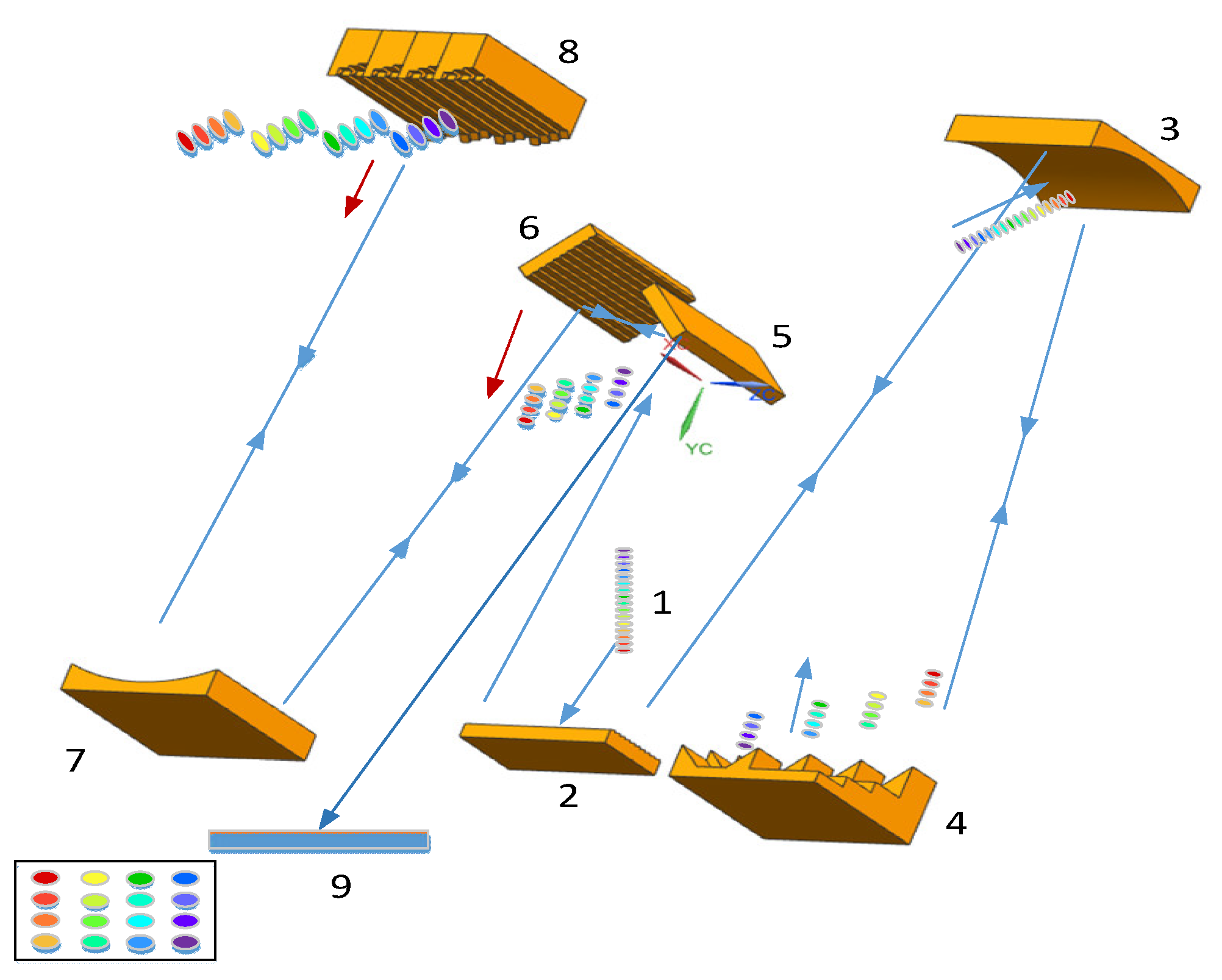
2.1. Composition of All-Optical Spatial Mapping Module

The schematic diagram of a two-dimensional (2D) all-optical spatial mapping module is shown in Figure 1. The whole device consists of two orthogonal modulation modules, which include a one-dimensional diffraction grating, a cylindrical mirror, and a periscope array.
When the incident pulse is diffracted by grating dispersion and reflected by a cylindrical mirror, a series of transverse λ1λ4 spots is formed. The No. 1 periscope array shown in Figure 2 is composed of several array elements fixed together, and each single array is fixed on a flat substrate by a pair of triangular mirrors (with increasing spacing). The difference in thickness of the flat substrate is used to compensate for the optical path variation caused by the difference in distance of the triangular mirrors on different arrays. The λ1λ4 spot is modulated by the No. 1 periscope array and then returned to the diffraction grating via the cylindrical mirror. In the incident direction of the original grating, there is the transverse spatially separated λ1λ4 frame, and then it is incident to another group of the orthogonal spatial mapping module. The No. 2 periscope array is a modular splice of the No. 1 periscope array, which is orthogonal. In the same way, λ1 is subdivided into λ11, λ12, λ13, λ14 by grating dispersion and then modulated by the first module of the No. 2 periscope array, and the rest λ2, λ3, λ4 are also modulated in the corresponding module. Finally, a 4 × 4 two-dimensional frame image is formed at the detector by the cylindrical mirror reflection and diffraction grating dispersion combining beam.

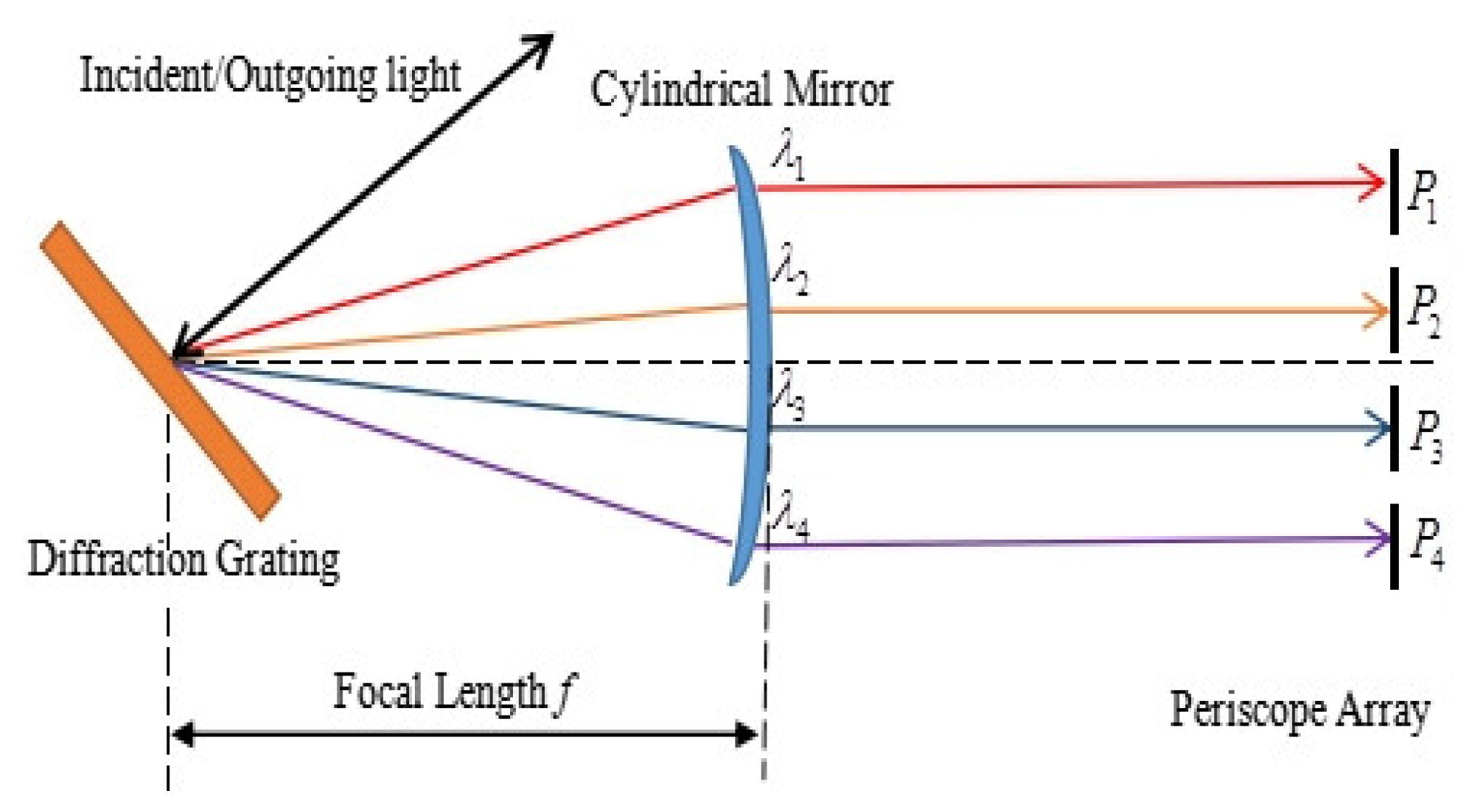
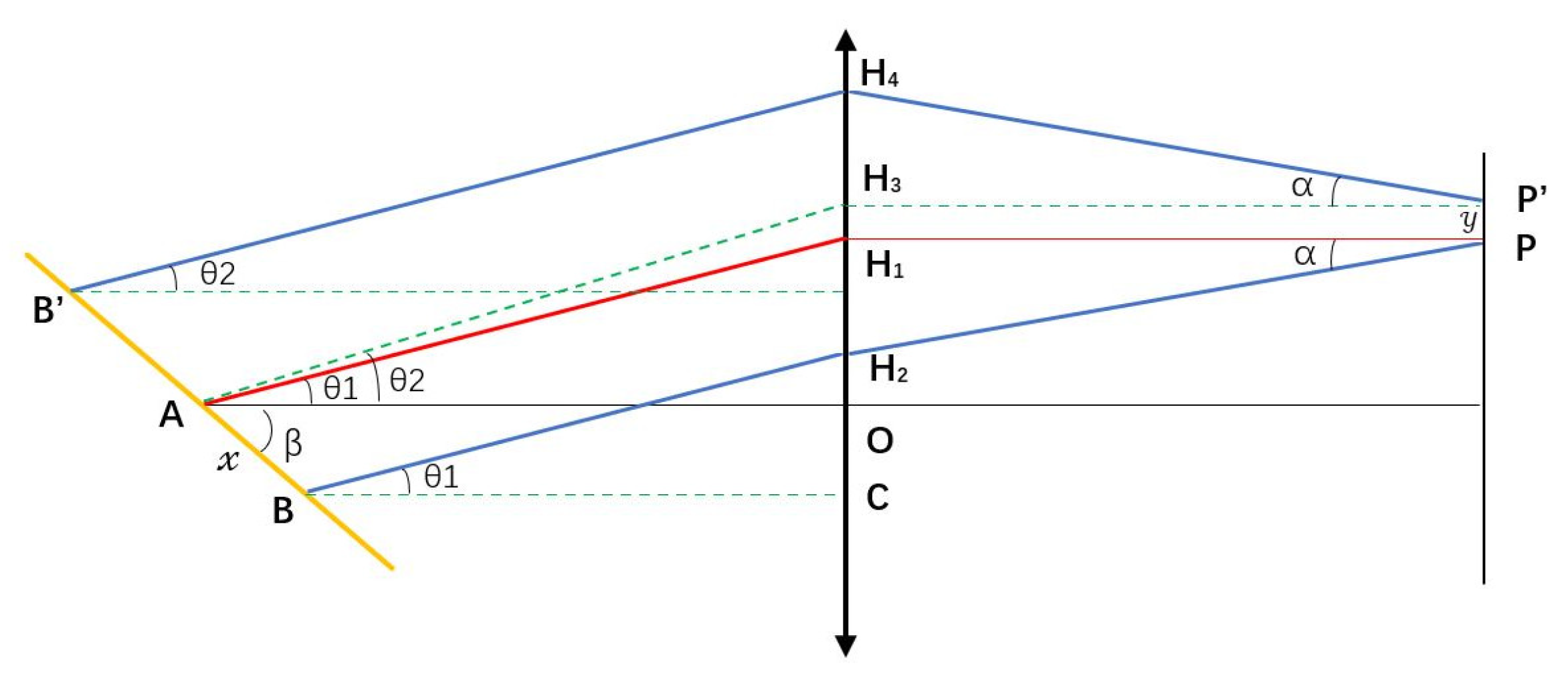
2.2. Theoretical Design of Two-Dimensional (2D) All-Optical Spatial Mapping Module

The schematic diagram of the one-dimensional spatial mapping module is shown in Figure 3. The cylindrical mirror is equivalent to the transmissive mirror, and separation points P1, P2, P3, and P4 on the periscope array correspond to the wavelengths λ1λ4 dispersed by diffraction grating.
According to the grating equation, the diffraction angle θ0 can be expressed as
θ o = arcsin m λ d sin θ i
In Equation (1), where d is the grating constant, θi is the angle of incidence, m is the diffraction level, λ is the wavelength, and f is the focal length of the cylindrical mirror, then the spatial distance between two neighboring wavelengths on the periscope array is:
δ 2 = f arcsin m λ 2 d sin θ i arcsin m λ 1 d sin θ i
Let δ = w. The relationship between the cylindrical mirror and the grating parameters can be expressed as follows:
f = δ · arcsin m λ 2 d sin θ i arcsin m λ 1 d sin θ i 1
According to Equation (3), the grating constant d, the angle of incidence θi, and the relationship with the focal length of the cylindrical mirror f can be determined. Let w0 = 6 mm, m = 1, λ1 = 790 nm, λ2 = 791.25 nm, and set the groove density of grating in the range of 500–2500 g/mm, and angle of incidence in the range of 20°–45°. The relation curve is plotted as shown in Figure 4, where the horizontal coordinate is the density of the grating lines, the vertical coordinate is the grating angle of incidence, and the contour line indicates the focal length of the cylindrical mirror. As can be seen from Figure 4, the focal length along with an increased density of grating lines decreases under the same grating angle of incidence, while the focal length along with an increased grating angle of incidence increases under the same density of grating lines.
The colored part in Figure 4 can meet the 6 mm line dispersion requirement and, considering the factors of fabrication difficulty, grating diffraction efficiency and component position interference, the final selected parameters are shown in Table 1:
The value of the width b of a single mirror on the periscope array can be expressed as:
b N = δ N 2
By using the grating and cylindrical mirror parameters as in Table 1, the b values of the No. 1 and No. 2 periscope array can be calculated as shown in Table 2 according to Equations (2) and (4):

2.3. Error Analysis of Two-Dimensional (2D) All-Optical Spatial Mapping Module

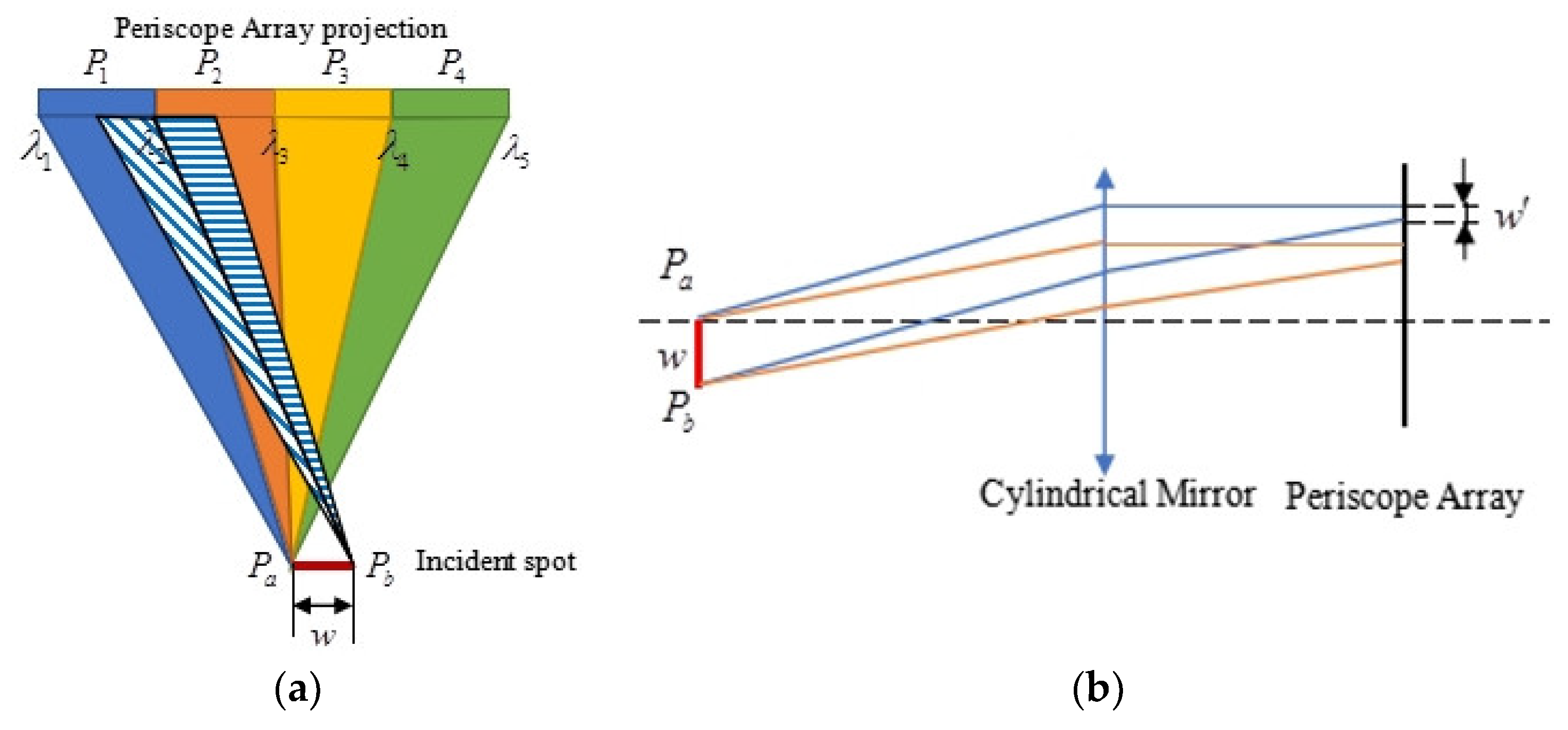
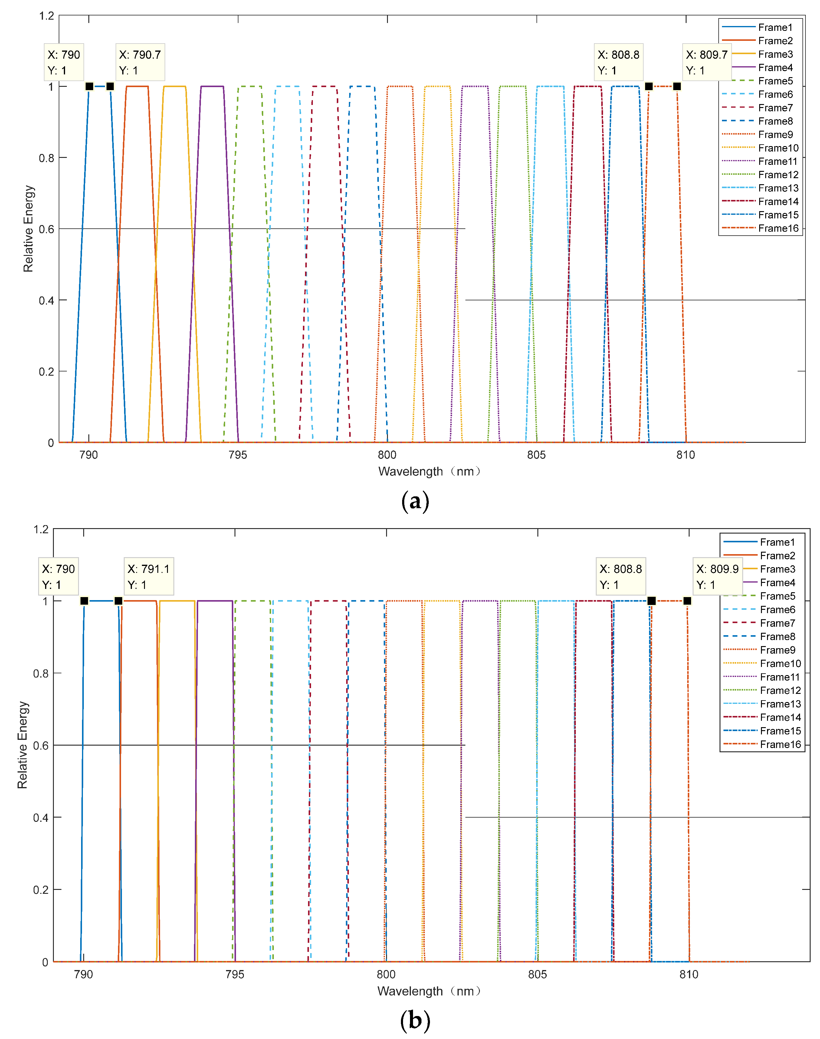
2.3.1. Analysis of Inter-Frame Energy Crosstalk Caused by Incident Beam Spot Width

When there is a width of incident spot rather than a point, inter-frame energy crosstalk will affect the imaging quality and spectral resolution of the module. The principal schematic is shown in Figure 5.
As shown in Figure 5a, in the plane formed by the direction of the grating line and the grating normal, the incident spot is projected as a line segment with projection size w, and the two endpoints are Pa and Pb. The parameters of the grating and the cylindrical mirrors above are designed based on the point of Pa, and the P1, P2, P3, and P4 points on the periscope array correspond to the wavelengths of λ1, λ2, λ3, and λ4, which are based on the dispersion of Pa. The wavelengths λ1λ4 no longer correspond to P1–P4 points on the periscope array for the other endpoint Pb.
The equivalent optical structure is shown in Figure 5b, where w′ represents offset at any wavelength. We set the offset w′ equal to w, and then the energy distribution of each frame is shown in Figure 6a, where the groove density of the grating is 1800 g/mm, the angle of incidence is 30°, and the focal length of the cylindrical mirror is 1067.5 mm. The analysis above ignores the diffraction efficiency of the grating and the reflectivity of each mirror surface. The horizontal coordinates represent wavelength, the vertical coordinates represent normalized energy, and the curves of different colors represent the normalized energy of each wavelength in a different frame. The flat top indicates the wavelength range without crosstalk; in Figure 6a, its ratio to the design bandwidth (1.25 nm) is between 56% and 72%. We believe the ideal situation is when the ratios are all greater than 85%. While the offset w′ is equal to w/6, the energy distribution of each frame is shown in Figure 6b, and the ratio is between 88% and 96%, which can better eliminate the effect of inter-crosstalk.
It should be additionally pointed out that, when w′ = 0, the wavelengths λ corresponding to the spots Pa to Pb are all incident on the same position of the periscope array. At this time, the positions of the incident spot, the cylindrical mirror, and the periscope array satisfy the 4f condition, in which inter-frame crosstalk no longer exists.

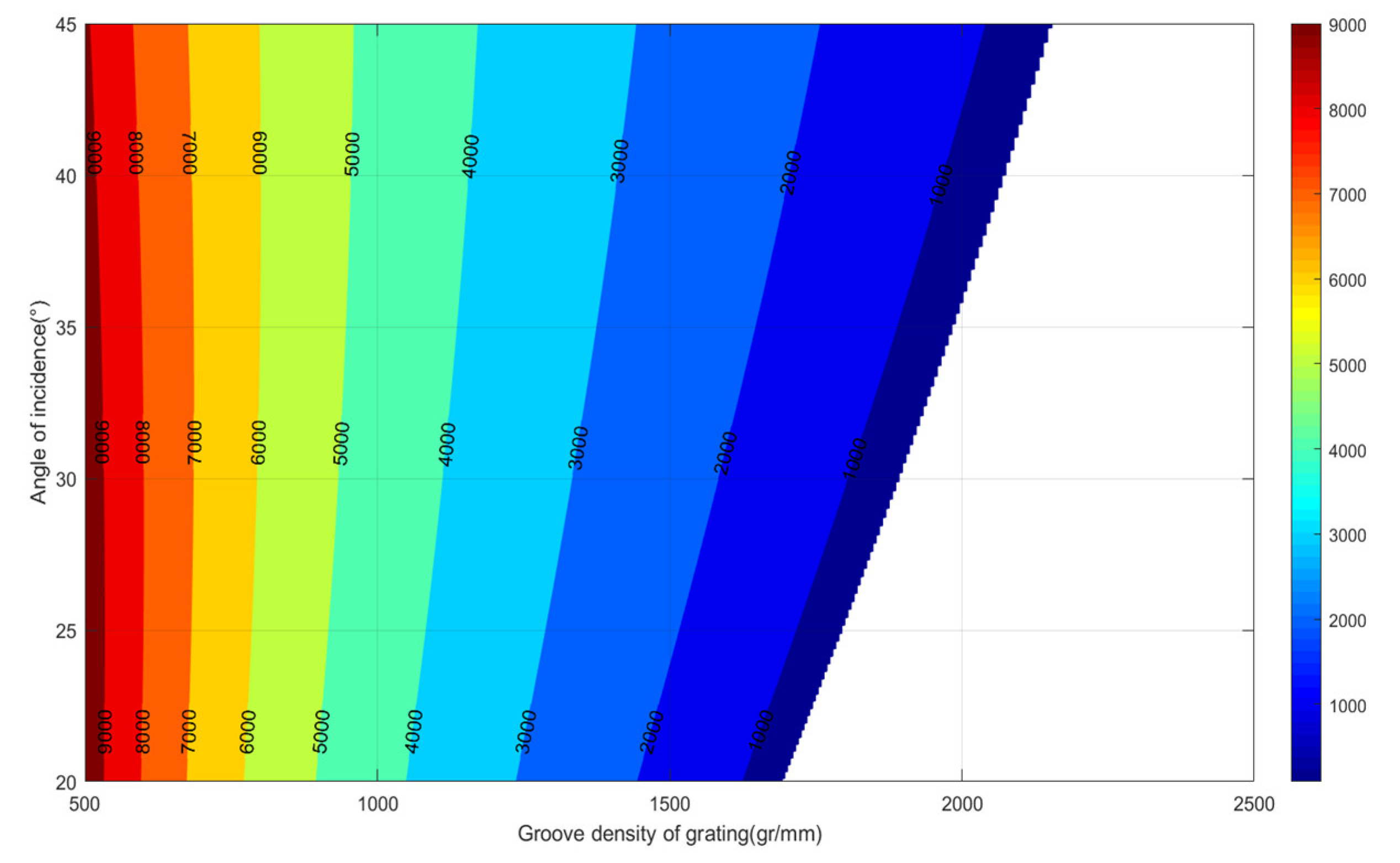
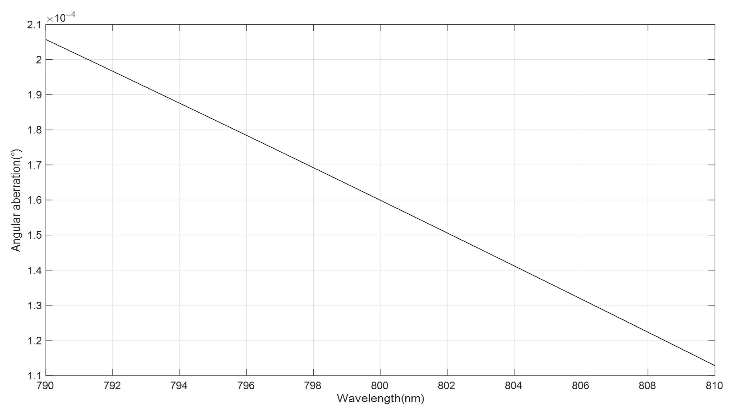
2.3.2. Analysis of Chromatic Aberration due to Incident Spot Width

Considering the characteristics of the periscope array, off-axis point imaging will cause object—image flip, which results in the spatial position of the image in each frame, so that the image converging at the grating again does not satisfy the achromatic condition. The actual optical path from the grating and the cylindrical mirrors to the periscope array is shown in Figure 7.
The distance of PP’ is the dispersion direction shift on the focal plane, which is set to be y, and the distance of AB is set to be x. Then we have:
H 1 H 2 = H 1 O H 2 O = H 1 O H 2 C O C
in which:
H 1 O = f tan θ 1 H 2 C = f x cos β tan θ 1 O C = x sin β
Coupling gives rise to:
H 1 H 2 = x cos β tan θ 1 + sin β
The relationship between θ1 and θ2 is:
tan θ 2 = f tan θ 1 + y f = tan θ 1 y f
in which:
y = L 1 tan α tan α = x f cos β tan θ 1 + sin β
where L1 is the offset distance in vertical direction after reflection by the periscope array, and α is the angle between light ray and the normal direction of the periscope array. Then we can obtain:
tan θ 2 = tan θ 1 L 1 x f 2 cos β tan θ 1 + sin β
For the position of the image as B′:
A B = x tan θ 1 + tan β tan θ 1 + tan β + y f   = x tan θ 1 + tan β tan θ 1 + tan β + L 1 x f 2 cos β tan θ + sin β
The distance between the B′ point position and point A can be determined using Equation (11), when the focal length f 2 » L1x, the outgoing and incident light rays satisfy the grating equation at the same time, and there is no chromatic aberration in our module. We can obtain:
β = π 2 arcsin m λ 800 n m d sin θ i
where λ800 nm is the central wavelength, and for the other wavelengths:
θ 1 = π 2 arcsin m λ d sin θ i β   = arcsin m λ 800 n m d sin θ i - arcsin m λ d sin θ i
From connective Equations (8) and (13), we can obtain:
tan θ 2 = tan arcsin m λ 800 n m d sin θ i - arcsin m λ d sin θ i   + L 1 x f 2 sin arcsin m λ 800 n m d sin θ i   × tan arcsin m λ 800 n m d sin θ i - arcsin m λ d sin θ i + cot arcsin m λ 800 n m d sin θ i
Let the grooving density of the grating 1/d = 1800 g/mm, angle of incidence θi = 30°, L1 = 8 mm, and x = 3 mm. Different wavelengths are diffracted by the grating and reflected back by the periscope array and cylindrical mirror. Its angle aberration after beam combination (Δθ) curve, between the outgoing angle after beam combination and the angle of incidence, is shown in Figure 8.
As can be seen from Figure 8, the angular aberration Δθ is within 0.0002057° under the condition of 1075 mm focal length, so chromatic aberration can be expressed as:
l = D tan Δ θ
where D is the total optical path, which is approximately equal to 4f, and finally we can compute the maximum chromatic aberration, which is equal to 15.44 um.

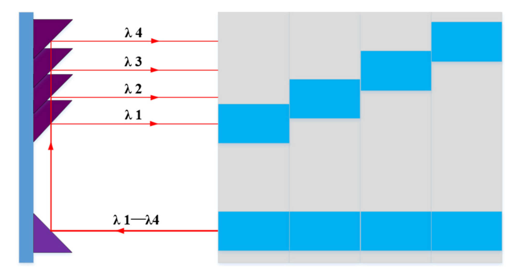
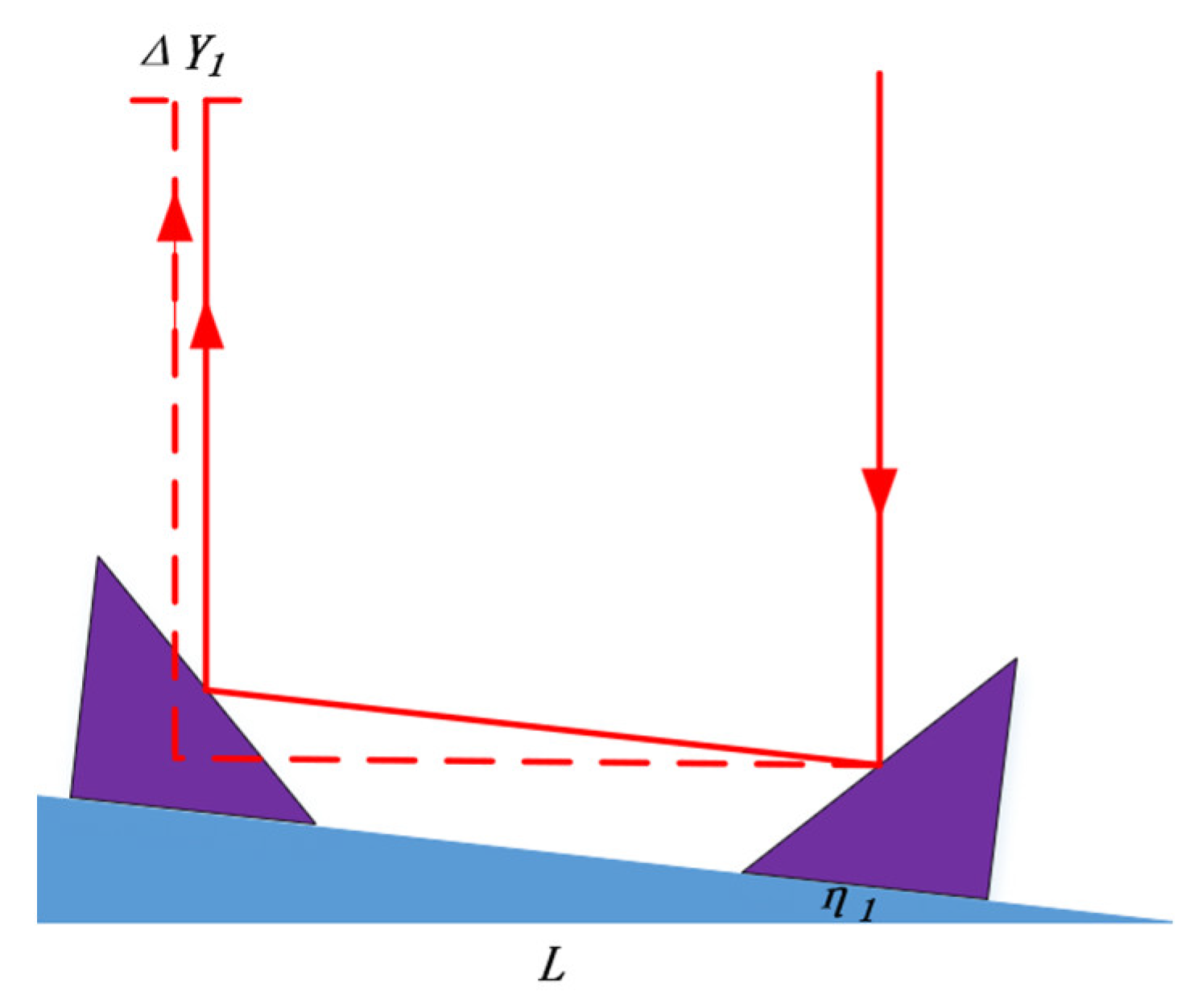
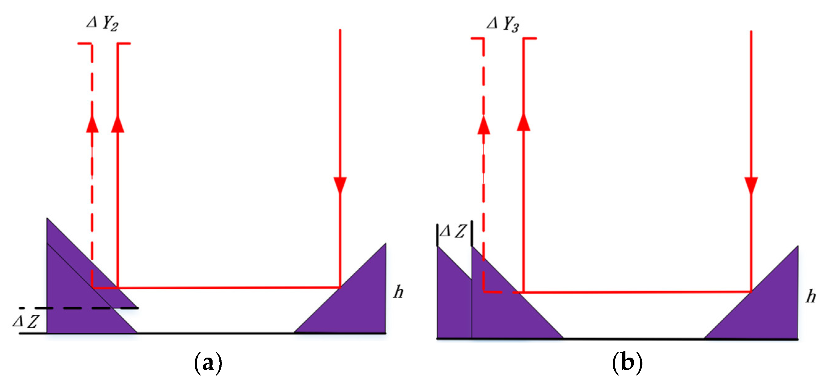
2.3.3. Analysis of Main Errors of the Periscope Array

Because of the long focal length of the module, any error of the periscope array may be more stringent, and the following analysis is carried out for the main errors of the periscope array fabrication.
  • Substrate angle error of the periscope array
The spot is shifted when there is a substrate angle error on the periscope array, and Figure 9 shows a schematic diagram of a substrate angle error:
Δ Y 1 = L × sin 2 η 1
where L represents the lateral distance from the midpoint of the step reflection unit to the rightmost side of the step, and η1 is the angular deviation as in Figure 9.
  • Triangular reflector traverse error of the periscope array
As shown in Figure 10a,b, the periscope array has a triangular reflector traverse error, which can lead to the transverse shift of the spot.
Let h be the side length of the isosceles right triangle and the spot size set to 6 mm. The spot transverse displacement can be expressed as:
Δ Y 2 , 3 1 2 ( h 3 )
  • Triangular reflector angle error of the periscope array
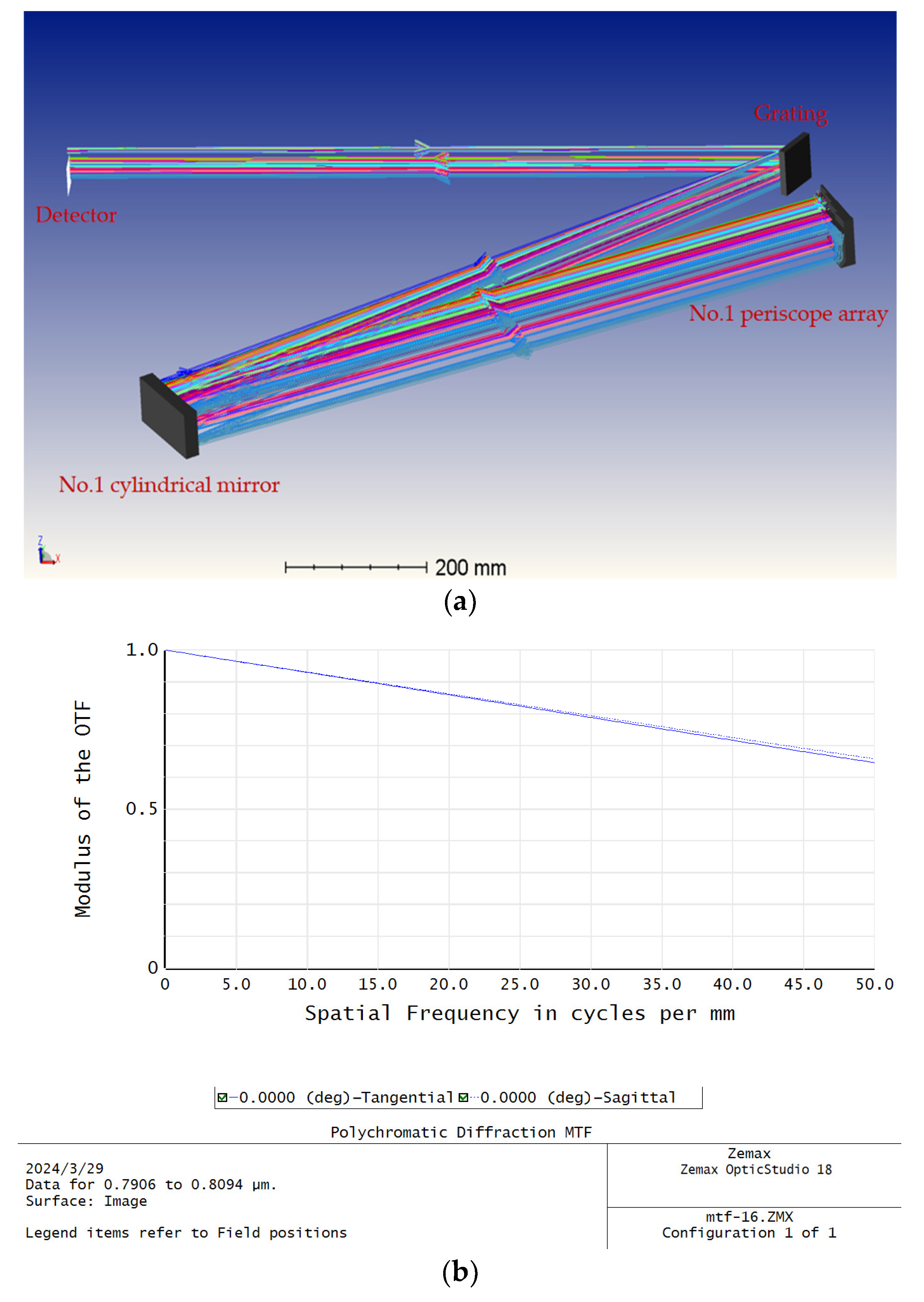
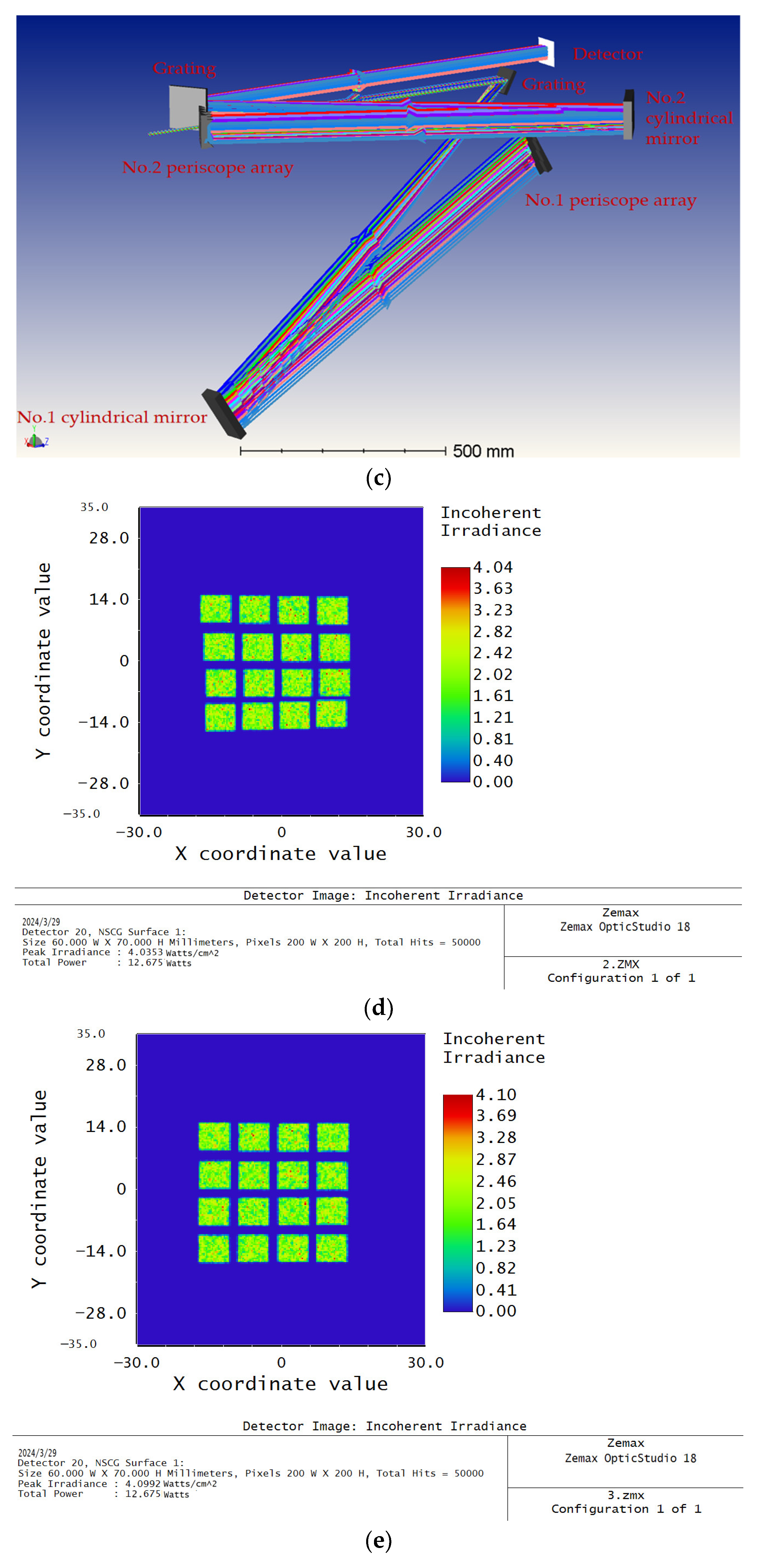
As shown in Figure 11a, if the reflector of the periscope array has an angle error that is around the normal, then the spot offset can be expressed as:
Δ Y 4 = 2 f tan η 2
Figure 11b shows the schematic diagram of the top-view principal of a triangular reflector, and the spot offset can be expressed as:
Δ Y 5 = b n tan η 3
The total error can be expressed as:
Δ Y = i = 1 5 Y i
We use the distance between adjacent frame boundaries (1.5 mm) as the total error ΔY constraint and, with comprehensive consideration of the sensitivity of the error and the level of fabrication, the error is distributed and tightened as shown in Table 3.

3. Results

The technical parameters, such as in Table 1 and Table 2, are selected according to the above theoretical model, and the two-dimensional (2D) all-optical spatial mapping module is designed using ZEMAX software. A four-frame transverse module is constructed as shown in Figure 12a, and the MTF of the transverse module in sequence mode is shown in Figure 12b. It reaches 0.64 at 50 lp/mm, so the 50 lp/mm MTF of a two-dimensional module can be estimated to be above 0.3. The complete optical structure is shown in Figure 12c, and the spot distribution on the image plane of the complete optical structure is shown in Figure 12d. The design results show 1.25 nm spectral resolution and 16 wavelengths with the 4 × 4 frame arrangement on the detector. It should be explained that the unequal spacing of each frame is due to the non-linearity of grating dispersion. Fine tuning of the angle of the corresponding glass substrate of the periscope array allows for an approximate equidistant arrangement, as shown in Figure 12e.
The final result of our module design meets the indicators shown in Table 4:

4. Conclusions

To solve the problems of fewer frames, lower spectral resolution, and lower detector sensor utilization, a two-dimensional (2D) all-optical spatial mapping module is proposed, and the optical parameters model based on our optical structure is established. The theoretical analysis of the inter-frame energy crosstalk caused by incident beam spot width, chromatic aberration, and main errors of the periscope array has been conducted. The results show that an offset w′ is equal to w/6, and crosstalk ratio is between 88% and 96%, which can better eliminate the effect of inter-crosstalk. The chromatic aberration caused by the width of the incident spot maximum value is 15.44 um, which is almost negligible. The angle error of the triangular mirror up to 0.01° is the most stringent among the fabrication errors of the periscope array. The design of our module can achieve a 16-frame image, 1.25 nm spectral resolution, and 0.3 at 50 lp/mm. Compared with the one-dimensional structure, the indexes of 6 frames and 3.33 nm spectral resolution are significantly improved, and almost equivalent to that of the slicing mirrors module’s 18 frames and 1.94 nm spectral resolution, while one ultra-fast image sensor was saved.

Supplementary Materials

The following supporting information can be downloaded at: https://www.mdpi.com/article/10.3390/s24072219/s1. The optical structure of a two-dimensional (2D) all-optical spatial mapping module is stored as a Zemax file in the supplementary material.

Author Contributions

Original draft by Z.M.; Review and editing by H.Y.; Formal analysis by K.C.; Software by Y.Y.; Data curation by C.T. All authors have read and agreed to the published version of the manuscript.

Funding

We are grateful for the support of the National Natural Science Foundation of China (NSFC) (62205331); Technology cooperation and industrialization between Jilin Province and Chinese Academy of Sciences (2021SYHZ0049); Jilin Province Science and Technology Development Plan (222637XM010499055); Suzhou Science and Technology Plan Project (ZXL2022478); Jiangsu Province High level Talent Introduction Plan for Innovation and Entrepreneurship Project (JSSCRC2022461).

Institutional Review Board Statement

Not applicable.

Informed Consent Statement

Not applicable.

Data Availability Statement

Data are contained within the article and Supplementary Materials.

Conflicts of Interest

The authors declare no conflicts of interest.

References

  1. Nakagawa, K.; Iwasaki, A.; Oishi, Y.; Horisaki, R.; Tsukamoto, A.; Nakamura, A.; Hirosawa, K.; Liao, H.; Ushida, T.; Goda, K. Sequentially timed all-optical mapping photography (STAMP). Nat. Photonics 2014, 8, 695–700. [Google Scholar] [CrossRef]
  2. Yuan, X.D.; Li, Z.X.; Zhou, J.H.; Liu, S.; Wang, D.; Lei, C. Hybrid-plane spectrum slicing for sequentially timed all-optical mapping photography. Opt. Lett. 2022, 47, 4822–4825. [Google Scholar] [CrossRef] [PubMed]
  3. Nemoto, H.; Suzuki, T.; Kannari, F. Extension of time window into nanoseconds in single-shot ultrafast burst imaging by spectrally sweeping pulses. Appl. Opt. 2020, 59, 5210–5215. [Google Scholar] [CrossRef] [PubMed]
  4. Bhat, V.N.; Thomas, A.S.; Bhattacharyya, A.; Tiwari, V. Rapid scan white light pump–probe spectroscopy with 100 kHz shot-to-shot detection. Opt. Contin. 2023, 2, 1981–1995. [Google Scholar] [CrossRef]
  5. Tang, J.C.; Sun, H.; Zhang, Q.Y.; Dai, X.C.; Wang, Z.; Ning, C.Z. Helicity-resolved Pump-Probe Observation of Biexciton Fine Structures in Monolayer Molybdenum Ditelluride. QELS Fundam. Sci. 2021. [Google Scholar] [CrossRef]
  6. Li, Y.H.; Tian, J.S.; Li, D.D.U. Theoretical investigations of a modified compressed ultrafast photography method suitable for single-shot fluorescence lifetime imaging. Appl. Opt. 2021, 60, 1476–1483. [Google Scholar] [CrossRef] [PubMed]
  7. Gan, H.Q.; Huang, Y.B.; Wang, F.; Li, H.Y.; Li, Y.L.; Huang, Z.X. l1 norm based sparse reconstruction approach to compressed ultrafast photography of velocity interferometer system for any reflector. Opt. Lett. 2023, 48, 5205–5208. [Google Scholar] [CrossRef] [PubMed]
  8. Matlis, N.H.; Axley, A.; Leemans, W.P. Single-shot ultrafast tomographic imaging by spectral multiplexing. Nat. Commun. 2012, 3, 1111. [Google Scholar] [CrossRef] [PubMed]
  9. Hodge, D.S.; Leong, N.F.T.; Pandolfi, S.; Kurzer-Ogul, K.; Montgomery, D.S.; Aluie, H.; Bolme, C.; Carver, T.; Cunningham, E.; Curry, C.B.; et al. Multi-frame, ultrafast, x-ray microscope for imaging shockwave dynamics. Opt. Express 2022, 30, 38405–38422. [Google Scholar] [CrossRef] [PubMed]
  10. Liu, J.; Cong, S.; Song, Y.; Chen, S.; Wu, D. Flow structure and acoustics of underwater imperfectly expanded supersonic gas jets. Shock. Waves 2022, 32, 283–294. [Google Scholar] [CrossRef]
  11. Burch, A.D.; Paudel, B.; Kang, K.T.; Lee, M.C.; Chen, A.P.; Zhu, J.X.; Prasankumar, R.P.; Hilton, D.J. Ultrafast Magnetic Field-Dependent Dynamics in the High-Temperature Superconductor La2−xSrxCuO4. In Proceedings of the CLEO: Applications and Technology, San Jose, CA, USA, 9–14 May 2021; Optica Publishing Group: Washington, DC, USA, 2021; p. JTh3A.88. [Google Scholar]
  12. Lin, P.; Li, C.; Flores-Valle, A.; Wang, Z.; Zhang, M.; Cheng, R.; Cheng, J.X. Tilt-angle stimulated Raman projection tomography. Opt. Express 2022, 30, 37112–37123. [Google Scholar] [CrossRef] [PubMed]
  13. Hall, C.R.; Collado, J.T.; Iuliano, J.N.; Adamczyk, K.; Lukacs, A.; Greetham, G.M.; Sazanovich, I.; Tonge, P.J.; Meech, S.R. Ultrafast Protein Dynamics Probed by Site Specific Transient IR Spectroscopy. In Proceedings of the 22nd International Conference on Ultrafast Phenomena 2020, Washington, DC, USA, 16–19 November 2020. [Google Scholar]
  14. Baikie, T.K.; Wey, L.T.; Lawrence, J.M.; Medipally, H.; Reisner, E.; Nowaczyk, M.M.; Friend, R.H.; Howe, C.J.; Schnedermann, C.; Rao, A.K.; et al. Photosynthesis re-wired on the pico-second timescale. Nature 2023, 615, 836–840. [Google Scholar] [CrossRef] [PubMed]
  15. Nakagawa, K.; Iwasaki, A.; Oishi, Y.; Horisaki, R.; Tsukamoto, A.; Nakamura, A.; Hirosawa, K.; Liao, H.E.; Ushida, T.; Goda, K.; et al. Motion Picture Femtophotography with Sequentially Timed All-optical Mapping Photography. In Proceedings of the Conference on Lasers and Electro-Optics 2015, San Jose, CA, USA, 10–15 May 2015. [Google Scholar]
  16. Tamamitsu, M.; Nakagawa, K.; Horisaki, R.; Iwasaki, A.; Oishi, Y.; Tsukamoto, A.; Kannari, F.; Sakuma, I.; Goda, K. Design for sequentially timed all-optical mapping photography with optimum temporal performance. Opt. Lett. 2015, 40, 633–636. [Google Scholar] [CrossRef] [PubMed]
  17. Suzuki, T.; Isa, F.; Fujii, L.; Hirosawa, K.; Nakagawa, K.; Goda, K.; Sakuma, I.; Kannari, F. Sequentially timed all-optical mapping photography (STAMP) utilizing spectral filtering. Opt. Express 2015, 23, 249960. [Google Scholar] [CrossRef] [PubMed]
  18. Suzuki, T.; Hida, R.; Yamaguchi, Y.; Nakagawa, K.; Saiki, T.; Kannari, F. Single-shot 25-frame burst imaging of ultrafast phase transition of Ge2Sb2 Te5 with a subpicosecond resolution. Appl. Phys. Express 2017, 10, 092502. [Google Scholar] [CrossRef]
  19. Saiki, T.; Hosobata, T.; Kono, Y.; Takeda, M.; Ishijima, A.; Tamamitsu, M.; Kitagawa, Y.; Goda, K.; Morita, S.-Y.; Ozaki, S.; et al. Sequentially timed all-optical mapping photography boosted by a branched 4f system with a slicing mirror. Opt. Express 2020, 28, 31914–31922. [Google Scholar] [CrossRef] [PubMed]
  20. Nemoto, H.; Suzuki, T.; Kannari, F. Single-shot ultrafast burst imaging using an integral field spectroscope with a microlens array. Opt. Lett. 2020, 45, 5004–5007. [Google Scholar] [CrossRef] [PubMed]
  21. Li, Z.X.; Yuan, X.D.; Weng, Y.Y.; Wang, D.; Wang, S.Y.; Liu, S.; Zhao, Z.Q.; Lei, C. 2D spectrum slicing for sequentially timed all-optical mapping photography with 25 frames. Appl. Phys. Lett. 2023, 123, 141103. [Google Scholar] [CrossRef]
Figure 1. Schematic diagram of two-dimensional (2D) all-optical spatial mapping module.The arrow indicates the direction of light propagation, and the digital label represents the optical element that the light incident on successively: 1-incident pulsed light; 2-grating; 3-No.1 cylindrical mirror; 4-No. 1 periscope array; 5-mirrors; 6-grating; 7-No.2 cylindrical mirror; 8-No. 2 periscope array; 9-Detector.
Sensors 24 02219 g001
Figure 2. Schematic diagram of the periscope array with top view and front view.
Sensors 24 02219 g002
Figure 3. Schematic diagram of one-dimensional spatial mapping module.
Sensors 24 02219 g003
Figure 4. Relation curve of grooving density of grating 1/d, angle of incidence θi and focal length f of cylindrical mirror.
Sensors 24 02219 g004
Figure 5. (a) Schematic diagram of energy crosstalk at the vertical optical path cross-section; (b) schematic diagram of energy crosstalk at the cross-section of the optical path.
Sensors 24 02219 g005
Figure 6. (a) Energy distribution of each frame when w′ = w; (b) energy distribution of each frame when w′ = w/6.
Sensors 24 02219 g006
Figure 7. Schematic diagram of imaging characteristics of off-axis points of incident light spots.
Sensors 24 02219 g007
Figure 8. Relation curve of wavelength λ and angle aberration after beam combination Δθ.
Sensors 24 02219 g008
Figure 9. Schematic diagram of substrate angle error of the periscope array. The arrow indicates the direction of light propagation. The dashed line represents the ideal propagation direction, and the solid line represents the actual propagation direction when there is an error.
Sensors 24 02219 g009
Figure 10. (a) Schematic diagram of the triangular reflector traverse error of the periscope array in the direction of the outgoing light; (b) Schematic diagram of the triangular reflector traverse error of the periscope array in the vertical direction of the outgoing light.
Sensors 24 02219 g010
Figure 11. (a) Schematic diagram of pitch angle error of the triangular reflector. The arrow indicates the direction of light propagation. The dashed line represents the ideal propagation direction, and the solid line represents the actual propagation direction when there is an error; (b) schematic diagram of azimuth angle error of the triangular reflector, 1-4 represent different triangular reflectors, and A-D represent corresponding triangular reflectors, where C triangular reflector have an azimuth angle error.
Sensors 24 02219 g011
Figure 12. (a) Optical structure of one-dimensional (landscape orientation) all-optical spatial mapping module with different colors representing different wavelengths; (b) MTF curve of one-dimensional all-optical spatial mapping module; (c) optical structure of two-dimensional all-optical spatial mapping module with different colors representing different wavelengths; (d) spot diagram of two-dimensional all-optical spatial mapping module; (e) spot diagram of two-dimensional all-optical spatial mapping module after adjustment.
Sensors 24 02219 g012aSensors 24 02219 g012b
Table 1. Main parameters of grating and cylindrical mirror.
ParametersValue
Grating groove density1800 g/mm
Incidence angle of grating30°
Focal length of No. 1 cylindrical mirror 1067.5 mm
Focal length of No. 2 cylindrical mirror 1075 mm
Table 2. Value of b for the two periscope array.
ParametersValue
Value of b for the No. 1 periscope array24.535 mm
26.133 mm
28.114 mm
30.653 mm
Value of b for the No. 2 periscope array6 mm6.086 mm6.177 mm6.271 mm
6.371 mm6.475 mm6.585 mm6.702 mm
6.825 mm6.955 mm7.093 mm7.241 mm
7.398 mm7.566 mm7.747 mm7.942 mm
Table 3. Final numerical value of errors.
ParametersCalculated ValueFinal Value
Angle error of the glass substrate: η11.93°0.5°
Traverse error of the triangular mirror: ΔY2Y31.2 mm/1.2 mm0.1 mm/0.1 mm
Angle error of the triangular mirror: η2/η30.0258°/1.06°0.01°/0.1°
Table 4. Final indicator of two-dimensional all-optical spatial mapping module.
Indicator NameIndicator Value
Number of frames16 (4 × 4)
Size of single frame6 mm × 6 mm
Spectral Bandwidth20 nm (790–810 nm)
Spectral Resolution1.25 nm
MTF@50 lp/mm≥0.3
Disclaimer/Publisher’s Note: The statements, opinions and data contained in all publications are solely those of the individual author(s) and contributor(s) and not of MDPI and/or the editor(s). MDPI and/or the editor(s) disclaim responsibility for any injury to people or property resulting from any ideas, methods, instructions or products referred to in the content.

