
Impact of Channel Thickness and Doping Concentration for Normally-Off Operation in Sn-Doped β-Ga2O3 Phototransistors

Abstract

1. Introduction
2. Materials and Methods
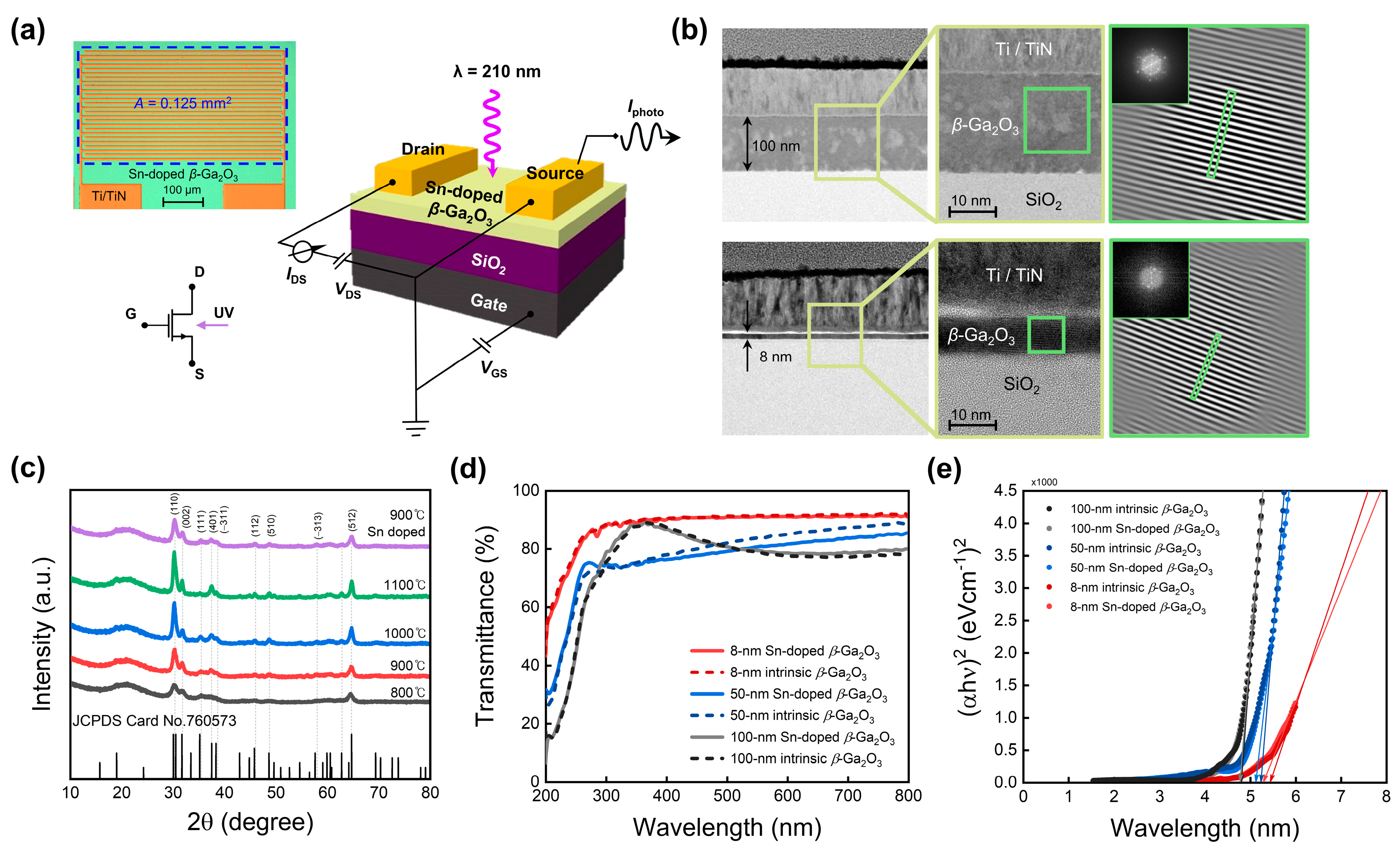
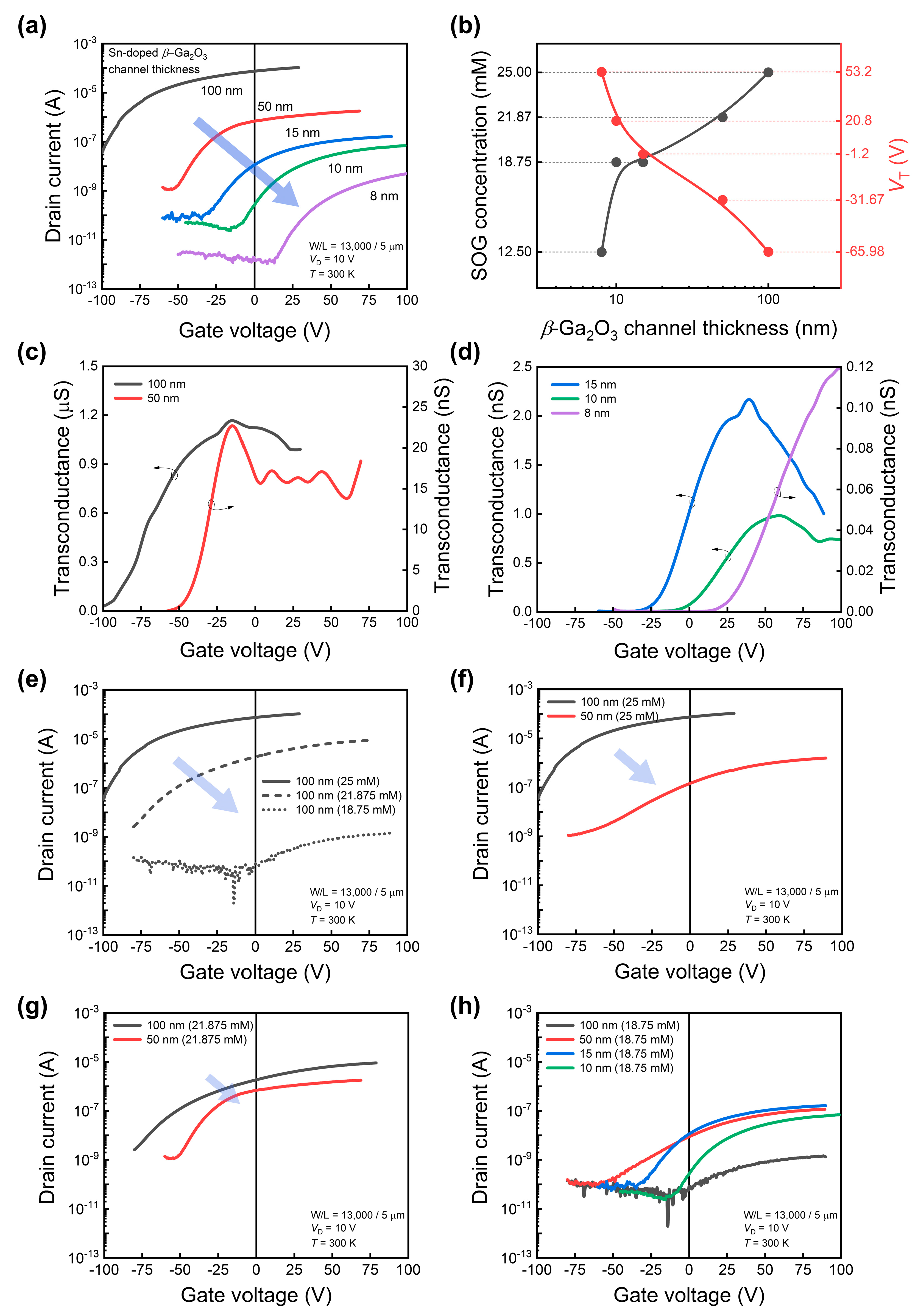
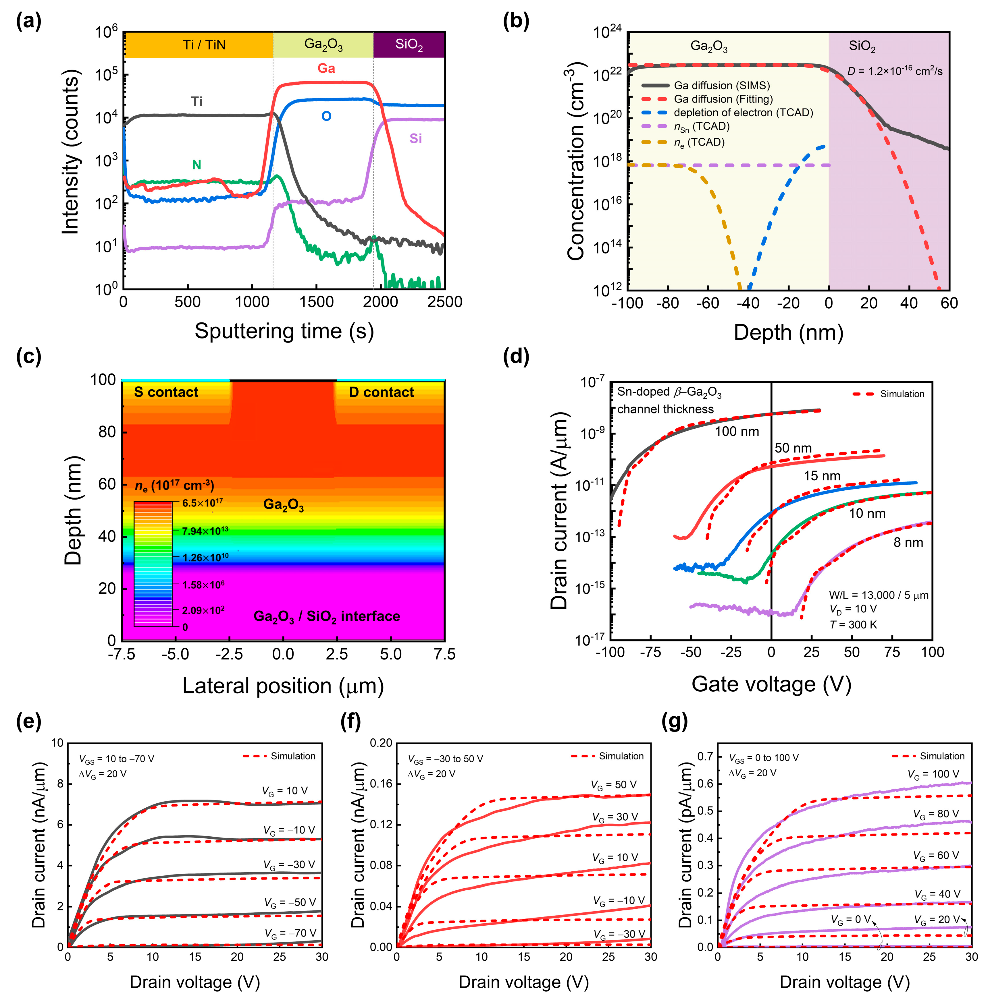
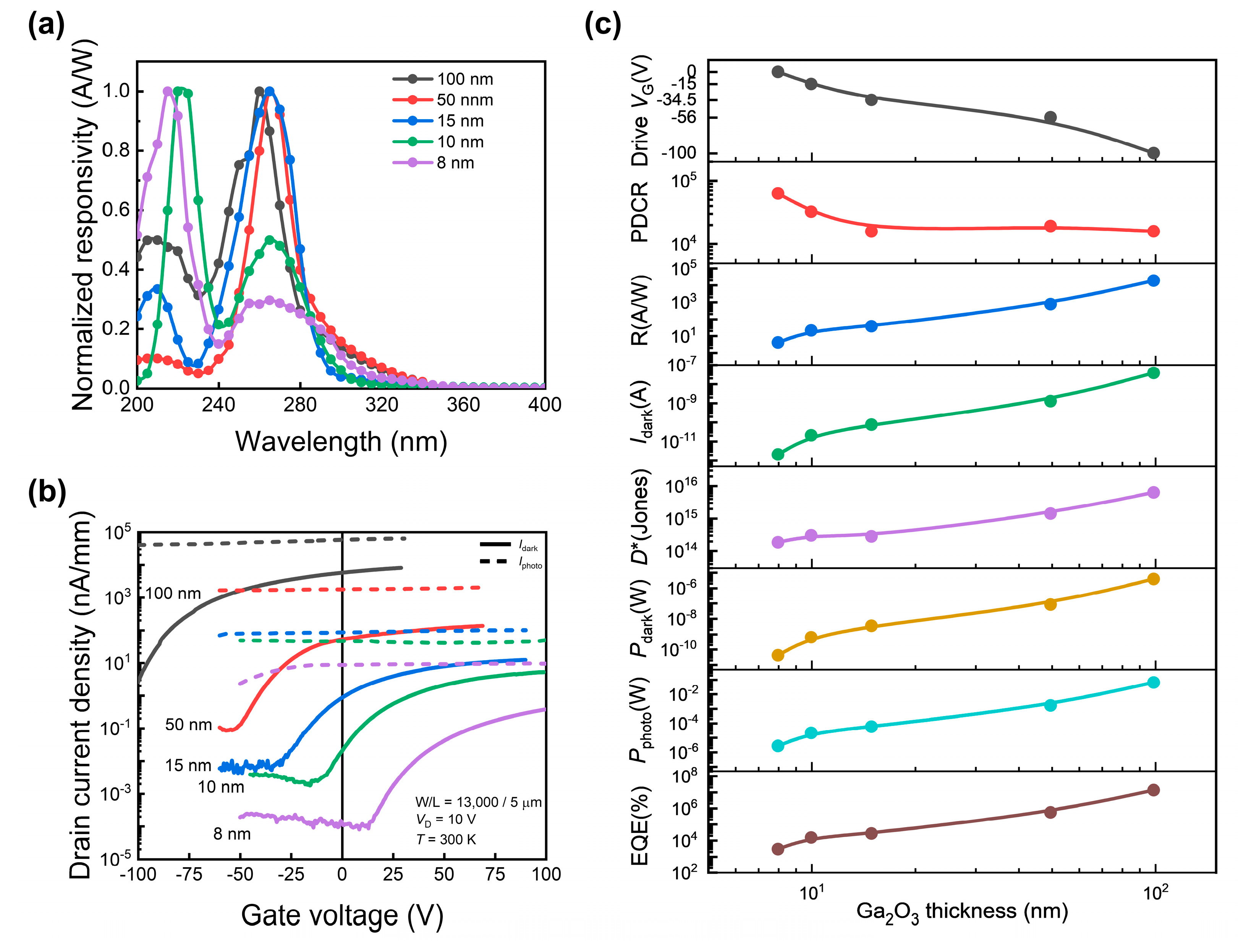
3. Results and Discussion
4. Conclusions
Author Contributions
Funding
Institutional Review Board Statement
Informed Consent Statement
Data Availability Statement
Conflicts of Interest
References
- Higashiwaki, M.; Jessen, G.H. Guest editorial: The dawn of gallium oxide microelectronics. Appl. Phys. Lett. 2018, 112, 060401. [Google Scholar] [CrossRef]
- Yamaguchi, K. First principles study on electronic structure of β-Ga2O3. Solid State Commun. 2004, 131, 739–744. [Google Scholar] [CrossRef]
- Dong, L.; Jia, R.; Xin, B.; Peng, B.; Zhang, Y. Effects of oxygen vacancies on the structural and optical properties of β-Ga2O3. Sci. Rep. 2017, 7, 40160. [Google Scholar] [CrossRef]
- Víllora, E.G.; Yamaga, M.; Inoue, T.; Yabasi, S.; Masui, Y.; Sugawara, T.; Fukuda, T. Optical spectroscopy study on β-Ga2O3. Jpn. J. Appl. Phys. 2002, 41, L622–L625. [Google Scholar] [CrossRef]
- Razeghi, M. Short-wavelength solar-blind detectors-status, prospects, and markets. Proc. IEEE 2002, 90, 1006–1014. [Google Scholar] [CrossRef]
- Sang, L.; Liao, M.; Sumiya, M. A Comprehensive review of semiconductor ultraviolet photodetectors: From thin film to one-dimensional nanostructures. Sensors 2013, 13, 10482–10518. [Google Scholar] [CrossRef] [PubMed]
- Guo, D.; Wu, Z.; Li, P.; An, Y.; Liu, H.; Guo, X.; Yan, H.; Wang, G.; Sun, C.; Li, L.; et al. Fabrication of β-Ga2O3 thin films and solar-blind photodetectors by laser MBE technology. Opt. Mater. Express 2014, 4, 1067. [Google Scholar] [CrossRef]
- Malik, M.; Iqbal, M.A.; Choi, J.R.; Pham, P.V. 2D Materials for efficient photodetection: Overview, mechanisms, performance and UV-IR range applications. Front. Chem. 2022, 10, 905404. [Google Scholar] [CrossRef]
- Yadav, P.V.K.; Ajitha, B.; Kumar Reddy, Y.A.; Sreedhar, A. Recent advances in development of nanostructured photodetectors from ultraviolet to infrared region: A Review. Chemosphere 2021, 279, 130473. [Google Scholar] [CrossRef]
- Arora, K.; Goel, N.; Kumar, M.; Kumar, M. Ultrahigh performance of self-powered β-Ga2O3 thin film solar-blind photodetector grown on cost-effective Si substrate using high-temperature seed layer. ACS Photonics 2018, 5, 2391–2401. [Google Scholar] [CrossRef]
- Bae, J.; Jeon, D.-W.; Park, J.-H.; Kim, J. High responsivity solar-blind metal-semiconductor-metal photodetector based on α-Ga2O3. J. Vac. Sci. Technol. A 2021, 39, 033410. [Google Scholar] [CrossRef]
- Kim, S.; Yoon, Y.; Seo, D.; Park, J.-H.; Jeon, D.-W.; Hwang, W.S.; Shin, M. Alpha-phase gallium oxide-based UVC photodetector with high sensitivity and visible blindness. APL Mater. 2023, 11, 061107. [Google Scholar] [CrossRef]
- Mi, W.; Tang, J.; Chen, X.; Li, X.; Li, B.; Luo, L.; Zhou, L.; Chen, R.; Wang, D.; Zhao, J. Preparation and UV detection performance of Ti-doped Ga2O3/intrinsic-Ga2O3/p-Si PIN photodiodes. J. Mater. Sci. Mater. Electron. 2023, 34, 774. [Google Scholar] [CrossRef]
- Vasquez, J.M.T.; Ashai, A.; Lu, Y.; Khandelwal, V.; Rajbhar, M.; Kumar, M.; Li, X.; Sarkar, B. A self-powered and broadband UV PIN photodiode employing a NiOx layer and a β-Ga2O3 heterojunction. J. Phys. D Appl. Phys. 2023, 56, 065104. [Google Scholar] [CrossRef]
- Kim, H.; Kim, K.; Hong, J. High performance deep ultraviolet P-i-n self-powered photodetector based on p-NiO/i-β-Ga2O3/n-β-Ga2O3 with controlled a fermi level and used an intrinsic β-Ga2O3 Layer. IEEE Sens. J. 2024, 24, 17613–17621. [Google Scholar] [CrossRef]
- Nandi, A.; Rana, K.S.; Bag, A. Design and analysis of P-GaN/N-Ga2O3 based junction barrier Schottky diodes. IEEE Trans. Electron. Devices 2021, 68, 6052–6058. [Google Scholar] [CrossRef]
- Liu, Z.; Tang, W. A Review of Ga2O3 deep-ultraviolet metal–semiconductor Schottky photodiodes. J. Phys. D Appl. Phys. 2023, 56, 093002. [Google Scholar] [CrossRef]
- Suzuki, R.; Nakagomi, S.; Kokubun, Y.; Arai, N.; Ohira, S. Enhancement of responsivity in solar-blind β-Ga2O3 photodiodes with a Au Schottky contact fabricated on single crystal substrates by annealing. Appl. Phys. Lett. 2009, 94, 222102. [Google Scholar] [CrossRef]
- Watahiki, T.; Yuda, Y.; Furukawa, A.; Yamamuka, M.; Takiguchi, Y.; Miyajima, S. Heterojunction p-Cu2O/n-Ga2O3 diode with high breakdown voltage. Appl. Phys. Lett. 2017, 111, 222104. [Google Scholar] [CrossRef]
- Nakagomi, S.; Momo, T.; Takahashi, S.; Kokubun, Y. Deep ultraviolet photodiodes based on β-Ga2O3/SiC heterojunction. Appl. Phys. Lett. 2013, 103, 072105. [Google Scholar] [CrossRef]
- Chi, P.-F.; Lin, F.-W.; Lee, M.-L.; Sheu, J.-K. High-responsivity solar-blind photodetectors formed by Ga2 O3/p-GaN bipolar heterojunctions. ACS Photonics 2022, 9, 1002–1007. [Google Scholar] [CrossRef]
- Kim, S.; Oh, S.; Kim, J. Ultrahigh deep-UV sensitivity in graphene-gated β-Ga2O3 phototransistors. ACS Photonics 2019, 6, 1026–1032. [Google Scholar] [CrossRef]
- Liu, Z.; Zhang, M.; Yang, L.; Li, S.; Zhang, S.; Li, K.; Li, P.; Guo, Y.; Tang, W. Enhancement-mode normally-off β-Ga2O3:Si metal-semiconductor field-effect deep-ultraviolet phototransistor. Semicond. Sci. Technol. 2022, 37, 015001. [Google Scholar] [CrossRef]
- Yoon, Y.; Kim, Y.; Hwang, W.S.; Shin, M. Biological UV photoreceptors-inspired Sn-Doped polycrystalline β-Ga2O3 optoelectronic synaptic phototransistor for neuromorphic computing. Adv. Electron. Mater. 2023, 9, 2300098. [Google Scholar] [CrossRef]
- Yoon, Y.; Hwang, W.S.; Shin, M. Solar-blind ultrathin Sn-doped polycrystalline Ga2O3 UV phototransistor for normally off operation. Adv. Photonics Res. 2022, 3, 2100316. [Google Scholar] [CrossRef]
- Liang, H.; Han, Z.; Mei, Z. Recent progress of deep ultraviolet photodetectors using amorphous gallium oxide thin films. Phys. Status Solidi A 2021, 218, 2000339. [Google Scholar] [CrossRef]
- Xu, J.; Zheng, W.; Huang, F. Gallium oxide solar-blind ultraviolet photodetectors: A Review. J. Mater. Chem. C Mater. 2019, 7, 8753–8770. [Google Scholar] [CrossRef]
- Kaur, D.; Kumar, M. A strategic review on gallium oxide based deep-ultraviolet photodetectors: Recent progress and future prospects. Adv. Opt. Mater. 2021, 9, 2002160. [Google Scholar] [CrossRef]
- Wong, M.H.; Lin, C.-H.; Kuramata, A.; Yamakoshi, S.; Murakami, H.; Kumagai, Y.; Higashiwaki, M. Acceptor doping of β-Ga2O3 by Mg and N ion implantations. Appl. Phys. Lett. 2018, 113, 102103. [Google Scholar] [CrossRef]
- Kyrtsos, A.; Matsubara, M.; Bellotti, E. On the feasibility of p-Type Ga2O3. Appl. Phys. Lett. 2018, 112, 032108. [Google Scholar] [CrossRef]
- Neal, A.T.; Mou, S.; Rafique, S.; Zhao, H.; Ahmadi, E.; Speck, J.S.; Stevens, K.T.; Blevins, J.D.; Thomson, D.B.; Moser, N.; et al. Donors and deep acceptors in β-Ga2O3. Appl. Phys. Lett. 2018, 113, 062101. [Google Scholar] [CrossRef]
- Robertson, J.; Clark, S.J. Limits to doping in oxides. Phys. Rev. B 2011, 83, 075205. [Google Scholar] [CrossRef]
- Petti, L.; Münzenrieder, N.; Vogt, C.; Faber, H.; Büthe, L.; Cantarella, G.; Bottacchi, F.; Anthopoulos, T.D.; Tröster, G. Metal oxide semiconductor thin-film transistors for flexible electronics. Appl. Phys. Rev. 2016, 3, 021303. [Google Scholar] [CrossRef]
- Yu, X.; Marks, T.J.; Facchetti, A. Metal oxides for optoelectronic applications. Nat. Mater. 2016, 15, 383–396. [Google Scholar] [CrossRef] [PubMed]
- Walsh, A.; Butler, K.T. Prediction of electron energies in metal oxides. Acc. Chem. Res. 2014, 47, 364–372. [Google Scholar] [CrossRef]
- Kamimura, T.; Nakata, Y.; Wong, M.H.; Than, P.H.; Higashiwaki, M. Nitrogen-Doped Channel β-Ga2O3 MOSFET with Normally-Off Operation. In Proceedings of the 2019 Compound Semiconductor Week (CSW), Nara, Japan, 19–23 May 2019; p. 1. [Google Scholar]
- Chabak, K.D.; McCandless, J.P.; Moser, N.A.; Green, A.J.; Mahalingam, K.; Crespo, A.; Hendricks, N.; Howe, B.M.; Tetlak, S.E.; Leedy, K.; et al. Recessed-gate enhancement-mode β-Ga2O3 MOSFETs. IEEE Electron. Device Lett. 2018, 39, 67–70. [Google Scholar] [CrossRef]
- Kachhawa, P.; Chaturvedi, N. A simulation approach for depletion and enhancement mode in β-Ga2O3 MOSFET. IETE Tech. Rev. 2022, 39, 1410–1418. [Google Scholar] [CrossRef]
- Chen, X.; Li, F.; Hess, H.L. Trench gate β-Ga2O3 MOSFETs: A review. Eng. Res. Express 2023, 5, 012004. [Google Scholar] [CrossRef]
- Zhou, H.; Si, M.; Alghamdi, S.; Qiu, G.; Yang, L.; Peide, D.Y. High-Performance Depletion/Enhancement-mode β-Ga2O3 on Insulator (GOOI) Field-Effect Transistors with Record Drain Currents of 600/450 mA/mm. IEEE Electron. Device Lett. 2016, 38, 103–106. [Google Scholar] [CrossRef]
- Sharma, R.; Patnaik, A.; Sharma, P. Impact of doping concentration and recess depth to achieve enhancement mode operation in β-Ga2O3 MOSFET. Microelectron. J. 2023, 135, 105755. [Google Scholar] [CrossRef]
- Gurbán, S.; Sulyok, A.; Menyhárd, M.; Baradács, E.; Parditka, B.; Cserháti, C.; Erdélyi, Z. Interface induced diffusion. Sci. Rep. 2021, 11, 9308. [Google Scholar] [CrossRef] [PubMed]
- Laemmle, A.; Wuerz, R.; Schwarz, T.; Cojocaru-Mirédin, O.; Choi, P.P.; Powalla, M. Investigation of the diffusion behavior of sodium in Cu (In, Ga) Se2 layers. J. Appl. Phys. 2014, 115, 154501. [Google Scholar] [CrossRef]
- Yoon, Y.; Kim, S.; Lee, I.G.; Cho, B.J.; Hwang, W.S. Electrical and photocurrent properties of a polycrystalline Sn-doped β-Ga2O3 thin film. Mater. Sci. Semicond. Process. 2021, 121, 105430. [Google Scholar] [CrossRef]
- Higashiwaki, M.; Sasaki, K.; Murakami, H.; Kumagai, Y.; Koukitu, A.; Kuramata, A.; Yamakoshi, S. Recent progress in Ga2O3 power devices. Semicond. Sci. Technol. 2016, 31, 034001. [Google Scholar] [CrossRef]
- Kotecha, R.; Metzger, W.; Mather, B.; Narumanchi, S.; Zakutayev, A. Modeling and analysis of gallium oxide vertical transistors. ECS J. Solid State Sci. Technol. 2019, 8, Q3202. [Google Scholar] [CrossRef]
- Janowitz, C.; Scherer, V.; Mohamed, M.; Krapf, A.; Dwelk, H.; Manzke, R.; Van de Walle, C.G. Experimental electronic structure of In2O3 and Ga2O3. New J. Phys. 2011, 13, 085014. [Google Scholar] [CrossRef]
- Shockley, W.T.R.W.; Read, W.T., Jr. Statistics of the recombinations of holes and electrons. Phys. Rev. 1952, 87, 835. [Google Scholar] [CrossRef]
- Ma, N.; Tanen, N.; Verma, A.; Guo, Z.; Luo, T.; Xing, H.G.; Jena, D. Intrinsic electron mobility limits in β-Ga2O3. Appl. Phys. Lett. 2016, 109, 212101. [Google Scholar] [CrossRef]
- Park, J.; Hong, S.M. Simulation study of enhancement mode multi-gate vertical gallium oxide MOSFETs. ECS J. Solid State Sci. Technol. 2019, 8, Q3116. [Google Scholar] [CrossRef]
- Jang, C.H.; Atmaca, G.; Cha, H.Y. Normally-off β-Ga2O3 MOSFET with an epitaxial drift layer. Micromachines 2022, 13, 1185. [Google Scholar] [CrossRef]
- Xiao, X.; Liang, L.; Pei, Y.; Yu, J.; Duan, H.; Chang, T.-C.; Cao, H. Solution-processed amorphous Ga2O3:CdO TFT-type deep-UV photodetectors. Appl. Phys. Lett. 2020, 116, 192102. [Google Scholar] [CrossRef]
- Duan, H.; Javaid, K.; Liang, L.; Huang, L.; Yu, J.; Zhang, H.; Gao, J.; Zhuge, F.; Chang, T.-C.; Cao, H. Broadband optoelectronic synaptic thin-film transistors based on oxide semiconductors. Phys. Status Solidi Rapid Res. Lett. 2020, 14, 1900630. [Google Scholar] [CrossRef]
- Dongre, B.; Carrete, J.; Wen, S.; Ma, J.; Li, W.; Mingo, N.; Madsen, G.K. Combined treatment of phonon scattering by electrons and point defects explains the thermal conductivity reduction in highly-doped Si. J. Mater. Chem. 2020, 8, 1273–1278. [Google Scholar] [CrossRef]
- Turney, J.E.; McGaughey, A.J.; Amon, C.H. In-plane phonon transport in thin films. J. Appl. Phys. 2010, 107, 024317. [Google Scholar] [CrossRef]
- Cao, R.; Sun, K.; Liu, C.; Mao, Y.; Guo, W.; Ouyang, P.; Meng, Y.; Tian, R.; Xie, L.; Lü, X.; et al. Structurally Flexible 2D Spacer for Suppressing the Electron–Phonon Coupling Induced Non-Radiative Decay in Perovskite Solar Cells. Nanomicro Lett. 2024, 16, 178. [Google Scholar] [CrossRef]
- Ni, Y.; Zhang, S.; Sun, L.; Liu, L.; Wei, H.; Xu, Z.; Xu, W.; Xu, W. A low-dimensional hybrid pin heterojunction neuromorphic transistor with ultra-high UV sensitivity and immediate switchable plasticity. Appl. Mater. Today 2021, 25, 101223. [Google Scholar] [CrossRef]
- Gong, J.; Wei, H.; Ni, Y.; Zhang, S.; Du, Y.; Xu, W. Methylammonium halide-doped perovskite artificial synapse for light-assisted environmental perception and learning. Mater. Today Phys. 2021, 21, 100540. [Google Scholar] [CrossRef]
- Ahn, J.; Ma, J.; Lee, D.; Lin, Q.; Park, Y.; Lee, O.; Heo, J. Ultrahigh deep-ultraviolet responsivity of a β-Ga2O3/MgO heterostructure-based phototransistor. ACS Photonics 2021, 8, 557–566. [Google Scholar] [CrossRef]
- Qin, Y.; Long, S.; He, Q.; Dong, H.; Jian, G.; Zhang, Y.; Liu, M. Amorphous gallium oxide-based gate-tunable high-performance thin film phototransistor for solar-blind imaging. Adv. Electron. Mater. 2019, 5, 1900389. [Google Scholar] [CrossRef]
- Qin, Y.; Dong, H.; Long, S.; He, Q.; Jian, G.; Zhang, Y.; Liu, M. Enhancement-Mode β-Ga2O 3 Metal–Oxide–Semiconductor Field-Effect Solar-Blind Phototransistor with Ultrahigh Detectivity and Photo-to-Dark Current Ratio. IEEE Electron. Device Lett. 2019, 40, 742–745. [Google Scholar] [CrossRef]
- Xu, Y.; Cheng, Y.; Li, Z.; Feng, Q.; Zhang, Y.; Chen, D.; Hao, Y. High performance gate tunable solar blind ultraviolet phototransistors based on amorphous Ga2O3 films grown by mist chemical vapor deposition. Nano Sel. 2021, 2, 2112–2120. [Google Scholar] [CrossRef]
- Li, Z.; Feng, Z.; Xu, Y.; Feng, Q.; Zhu, W.; Chen, D.; Hao, Y. High performance β-Ga2O 3 solar-blind metal–oxide–semiconductor field-effect phototransistor with hafnium oxide gate dielectric process. IEEE Electron. Device Lett. 2021, 42, 545–548. [Google Scholar] [CrossRef]
- Yu, S.; Zhao, X.; Ding, M.; Tan, P.; Hou, X.; Zhang, Z.; Long, S. High-detectivity β-Ga2O3 microflake solar-blind phototransistor for weak light detection. IEEE Electron. Device Lett. 2021, 42, 383–386. [Google Scholar] [CrossRef]
- Kim, S.; Kim, J. Highly selective ozone-treated β-Ga2O3 solar-blind deep-UV photodetectors. Appl. Phys. Lett. 2020, 117, 261101. [Google Scholar] [CrossRef]
- Han, Z.; Liang, H.; Huo, W.; Zhu, X.; Du, X.; Mei, Z. Boosted UV photodetection performance in chemically etched amorphous Ga2O3 thin-film transistors. Adv. Opt. Mater. 2020, 8, 1901833. [Google Scholar] [CrossRef]
- Pintor-Monroy, M.I.; Reyes-Banda, M.G.; Avila-Avendano, C.; Quevedo-Lopez, M.A. Tuning electrical properties of amorphous Ga2O3 thin films for deep UV phototransistors. IEEE Sens. J. 2021, 21, 14807–14814. [Google Scholar] [CrossRef]
- Liu, Y.; Du, L.; Liang, G.; Mu, W.; Jia, Z.; Xu, M.; Song, A. Ga2O3 field-effect-transistor-based solar-blind photodetector with fast response and high photo-to-dark current ratio. IEEE Electron. Device Lett. 2018, 39, 1696–1699. [Google Scholar] [CrossRef]
- Roh, Y.; Heo, G.; Whang, S.E. A survey on data collection for machine learning: A big data-ai integration perspective. IEEE Trans. Knowl. Data Eng. 2019, 33, 1328–1347. [Google Scholar] [CrossRef]
- Uddin, S.; Lu, H. Dataset meta-level and statistical features affect machine learning performance. Sci. Rep. 2024, 14, 1670. [Google Scholar] [CrossRef]


| Planes | Lattice Spacing [Å] | Planes | Lattice Spacing [Å] | ||
|---|---|---|---|---|---|
| JCPDS | 8 nm Sn-Doped Polycrystalline β-Ga2O3 | JCPDS | 100 nm Sn-Doped Polycrystalline β-Ga2O3 | ||
| (−401) | 2.929 | 2.920 | (111) | 2.549 | 2.549 |
| (−111) | 2.675 | 2.665 | (−311) | 2.343 | 2.356 |
| (002) | 2.817 | 2.857 | (400) | 2.971 | 2.998 |
| (112) | 1.978 | 1.962 | (401) | 2.403 | 2.385 |
| β-Ga2O3 Thickness [nm] | SOG Solution Concentration [mM] | Doping Weight |
|---|---|---|
| 100 | 25 | 1 |
| 50 | 21.875 | 0.875 |
| 15 | 18.75 | 0.75 |
| 10 | 18.75 | 0.75 |
| 8 | 12.5 | 0.5 |
| Material Parameters | Values | Unit | Source |
| Dielectric constant | 10 | unitless | [45] |
| Electron affinity | 4 | eV | [46] |
| Electron density of state (300 K) | 3.72 × 10¹⁸ | cm−3 | [47] |
| Electron density of state (300 K) | 3.72 × 10¹⁸ | cm−3 | [47] |
| Shockley–Read–Hall Recombination (SRG) Model | Values | Unit | Source |
| Specifies SRH lifetime for electrons | 1.2 × 10⁻⁸ | s | [48] |
| Specifies SRH lifetime for holes | 1.2 × 10⁻⁸ | s | [48] |
| Parameter | β-Ga2O3 Thickness [nm] | ||||
|---|---|---|---|---|---|
| 100 | 50 | 15 | 10 | 8 | |
| VT [V] | −65.98 | −31.67 | −1.2 | 20.8 | 53.2 |
| Mobility [cm2/V∙s] | 3.81 × 10⁻³ | 5.23 × 10⁻⁵ | 7.6 × 10⁻⁶ | 2.89 × 10⁻⁶ | 3.94 × 10⁻⁷ |
| On–off ratio | - | 1.66 × 10³ | 2.93 × 10³ | 3.7 × 10³ | 4.73 × 10³ |
| Drive VG [V] | −100 | −56 | −34.5 | −15 | 0 |
| PDCR | 1.57 × 10⁴ | 1.90 × 10⁴ | 1.55 × 10⁴ | 3.20 × 10⁴ | 6.19 × 10⁴ |
| R [A/W] | 1.73 × 10⁴ | 7.08 × 10² | 34.2 | 19.4 | 3.7 |
| Idark [A] | 3.39 × 10⁻⁸ | 1.15 × 10⁻⁹ | 6.75 × 10⁻¹¹ | 1.86 × 10⁻¹¹ | 1.84 × 10⁻¹² |
| D* [Jones] | 5.87 × 10¹⁵ | 1.31 × 10¹⁵ | 2.60 × 10¹⁴ | 2.80 × 10¹⁴ | 1.71 × 10¹⁴ |
| Pdark [W] | 3.20 × 10⁻⁶ | 6.78 × 10⁻⁸ | 2.84 × 10⁻⁹ | 5.03 × 10⁻¹⁰ | 3.31 × 10⁻¹¹ |
| Pphoto [W] | 5.01 × 10⁻² | 1.29 × 10⁻³ | 4.42 × 10⁻⁵ | 1.61 × 10⁻⁵ | 2.05 × 10⁻⁶ |
| EQE [%] | 1.02 × 10⁷ | 4.18 × 10⁵ | 2.02 × 10⁴ | 1.14 × 10⁴ | 2.19 × 10³ |
| Channel Thickness [nm] | Drive VG [V] | R [A/W] | Idark [A] | PDCR | D* [Jones] | Ref. |
|---|---|---|---|---|---|---|
| 8 | 0 | 3.7 | 1.84 × 10⁻¹² | 6.19 × 10⁴ | 1.71 × 10¹⁴ | This work |
| 100 | −100 | 1.73 × 10⁴ | 3.39 × 10⁻⁸ | 1.57 × 10⁴ | 5.87 × 10¹⁵ | This work |
| 280 | −8 | 2.6 × 10³ | 1.2 × 10⁻¹³ | 6 × 10⁸ | 9.7 × 10¹³ | [22] |
| 270 | −20 | 2.4 × 10⁷ | 6.7 × 10⁻¹² | - | 1.7 × 10¹⁵ | [59] |
| 208 | −30 | 4.1 × 10³ | 2 × 10⁻¹¹ | - | 2.57 × 10¹³ | [60] |
| 200 | −5 | 3 × 10³ | 7 × 10⁻¹³ | 1.1 × 10⁶ | 1.3 × 10¹⁶ | [61] |
| 267 | −10 | 2.3 × 10³ | ≈1.5 × 10⁻⁹ | 6.67 × 10³ | 1.87 × 10¹⁴ | [62] |
| 112 | −27 | 1.43 × 10⁷ | ≈4.8 × 10⁻¹³ | 6.9 × 10⁷ | 1.1 × 10¹⁹ | [63] |
| 217 | −10 | 1.17 × 10⁵ | 2.7 × 10⁻¹⁴ | 1.08 × 10⁷ | 1.19 × 10¹⁸ | [64] |
| 381 | −39.5 | 1.93 × 10⁶ | 4.35 × 10⁻¹¹ | 3.1 × 10⁸ | 1.9 × 10¹⁵ | [65] |
| 400 | 10 | 5.67 × 10³ | ≈1 × 10⁻¹² | 5.7 × 10⁷ | 1.87 × 10¹⁵ | [66] |
| 59 | 0 | 1 × 10² | 1 × 10⁻¹³ | ≈3 × 10⁸ | 1 × 10¹⁵ | [67] |
| 30 | 0.2 | 2.17 | 1.61 × 10⁻¹² | ≈1 × 10⁵ | 1.71 × 10¹² | [52] |
| 142 | −20 | 4.79 × 10⁵ | 9.91 × 10⁻¹² | 1 × 10⁵ | 6.69 × 10¹⁴ | [68] |
Disclaimer/Publisher’s Note: The statements, opinions and data contained in all publications are solely those of the individual author(s) and contributor(s) and not of MDPI and/or the editor(s). MDPI and/or the editor(s) disclaim responsibility for any injury to people or property resulting from any ideas, methods, instructions or products referred to in the content. |
© 2024 by the authors. Licensee MDPI, Basel, Switzerland. This article is an open access article distributed under the terms and conditions of the Creative Commons Attribution (CC BY) license (https://creativecommons.org/licenses/by/4.0/).
Share and Cite
Yoon, Y.; Kim, Y.; Shin, M. Impact of Channel Thickness and Doping Concentration for Normally-Off Operation in Sn-Doped β-Ga2O3 Phototransistors. Sensors 2024, 24, 5822. https://doi.org/10.3390/s24175822
Yoon Y, Kim Y, Shin M. Impact of Channel Thickness and Doping Concentration for Normally-Off Operation in Sn-Doped β-Ga2O3 Phototransistors. Sensors. 2024; 24(17):5822. https://doi.org/10.3390/s24175822
Chicago/Turabian StyleYoon, Youngbin, Yongki Kim, and Myunghun Shin. 2024. "Impact of Channel Thickness and Doping Concentration for Normally-Off Operation in Sn-Doped β-Ga2O3 Phototransistors" Sensors 24, no. 17: 5822. https://doi.org/10.3390/s24175822
APA StyleYoon, Y., Kim, Y., & Shin, M. (2024). Impact of Channel Thickness and Doping Concentration for Normally-Off Operation in Sn-Doped β-Ga2O3 Phototransistors. Sensors, 24(17), 5822. https://doi.org/10.3390/s24175822