
Compact Back-End Electronics with Temperature Compensation and Efficient Data Management for In Situ SiPM-Based Radiation Detection


Abstract
1. Introduction
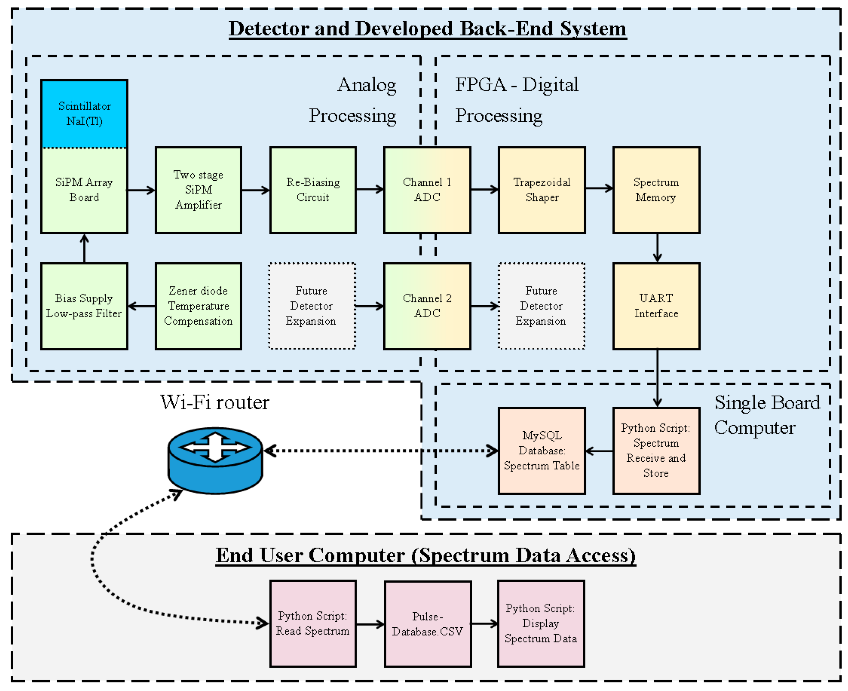
2. Detector Hardware Design
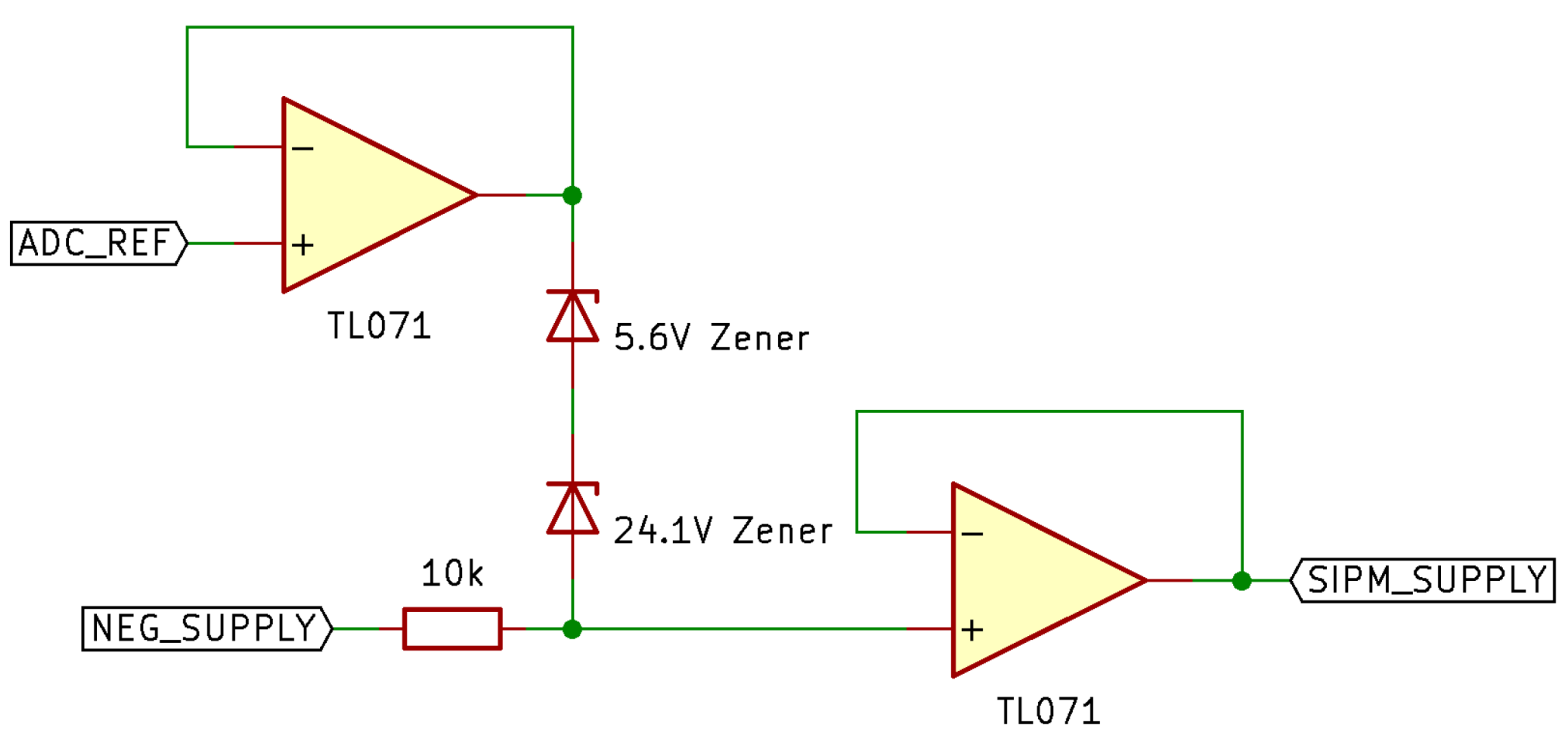
- The Zener Diode Temperature Compensation system has been developed to counter the drift in the gain in the SiPMs due to temperature changes.
- A Bias Supply Low-pass Filter is used to remove high frequency noise from the supply of the SiPM.
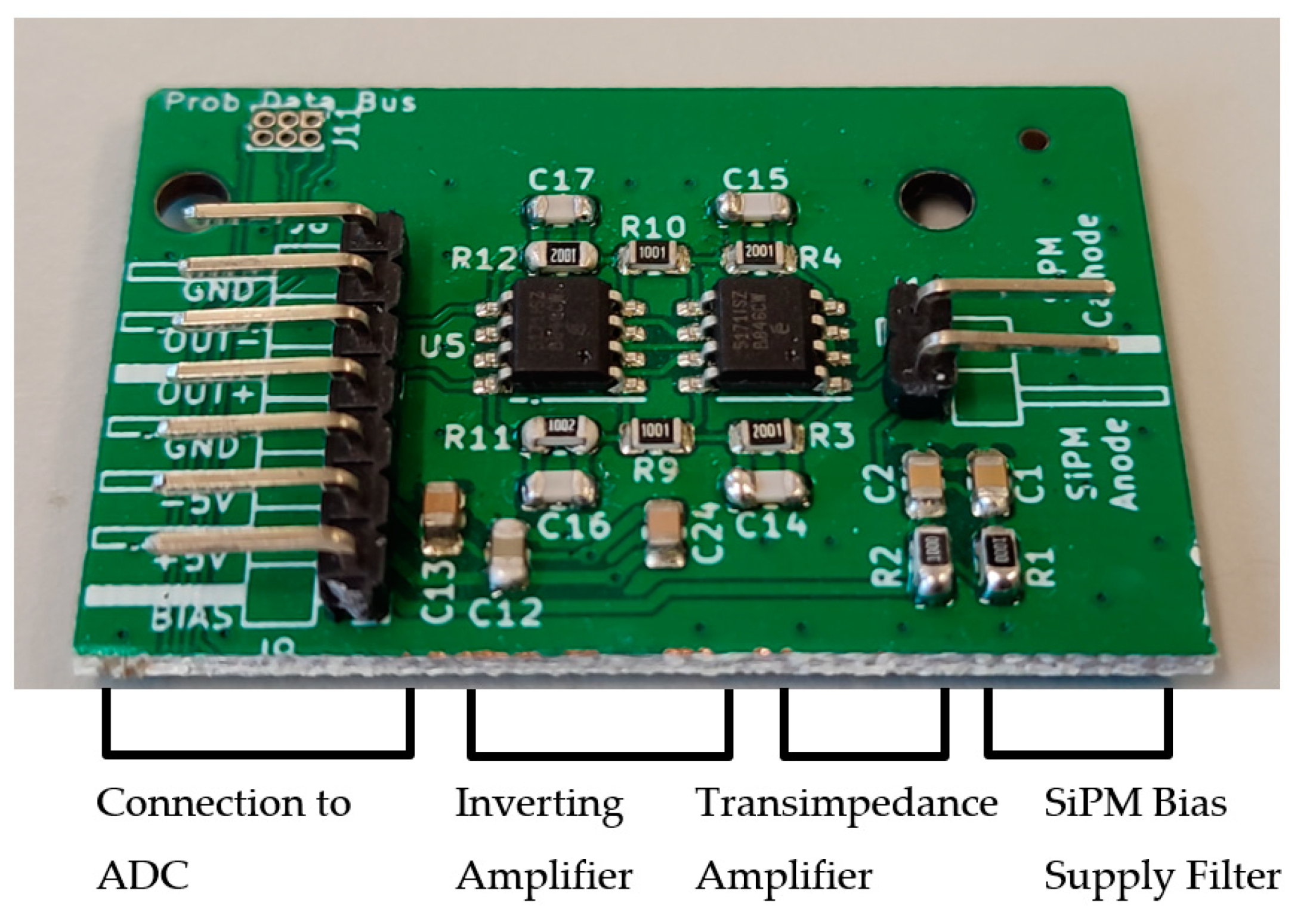
- A SiPM Array Board is a circuit board developed to hold a maximum of 17 SiPMs in an array in contact with the scintillator.
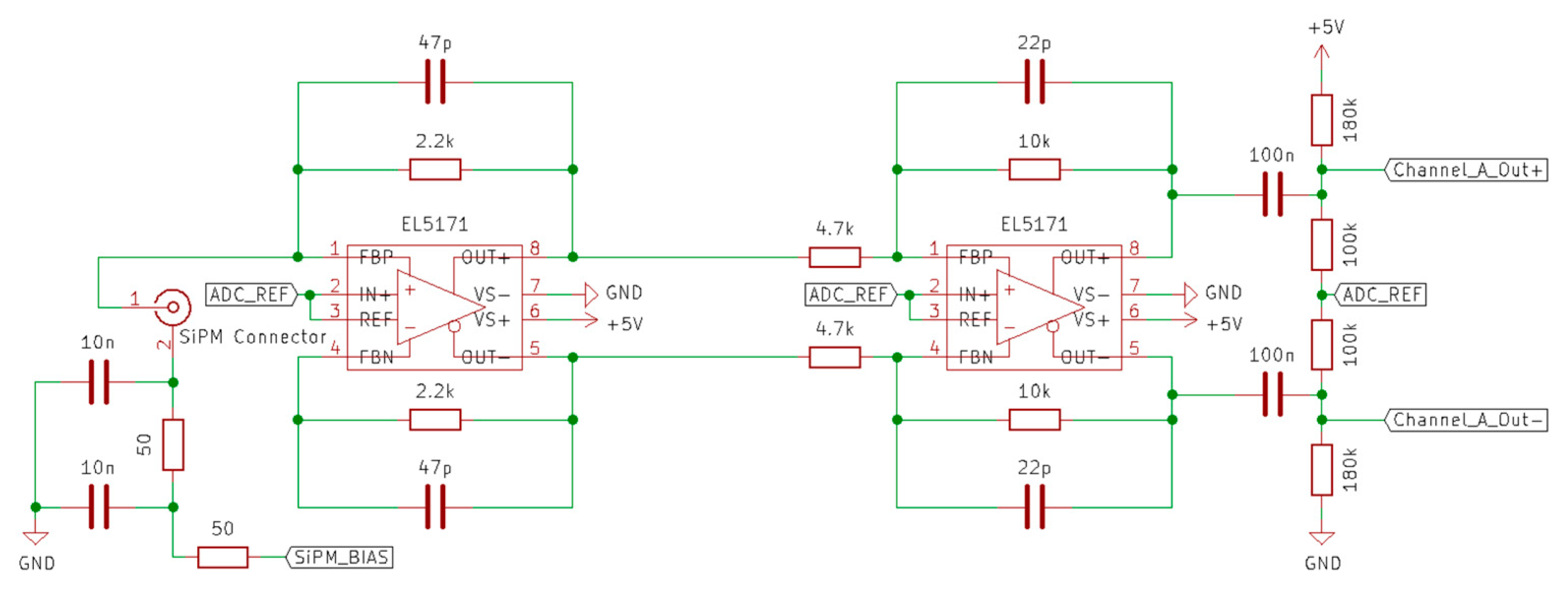
- The Two stage SiPM Amplifier converts current pulses from the SiPM into pulses of voltage that can be digitized for further analysis.
- The Re-Biasing Circuit removes dark voltage and adds a set bias to maximise ADC range.
- Channel 1 & 2 ADCs are integrated into a circuit board with the FPGA to digitize pulses from the SiPM.
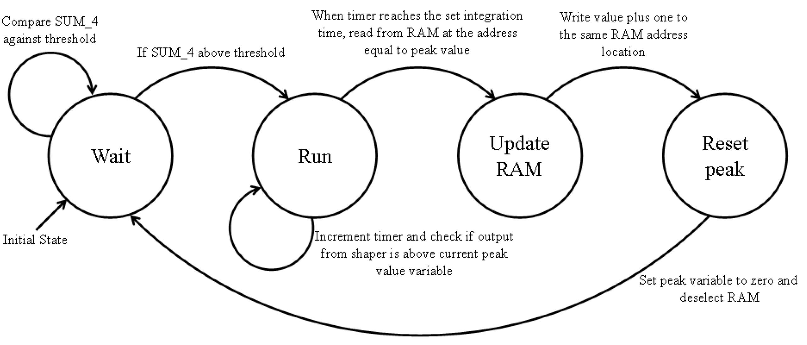
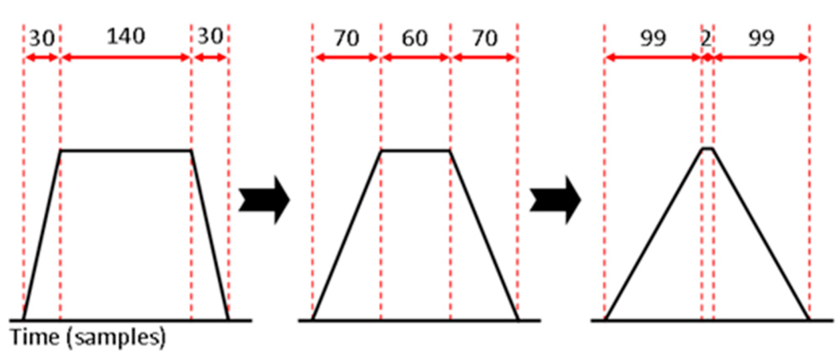
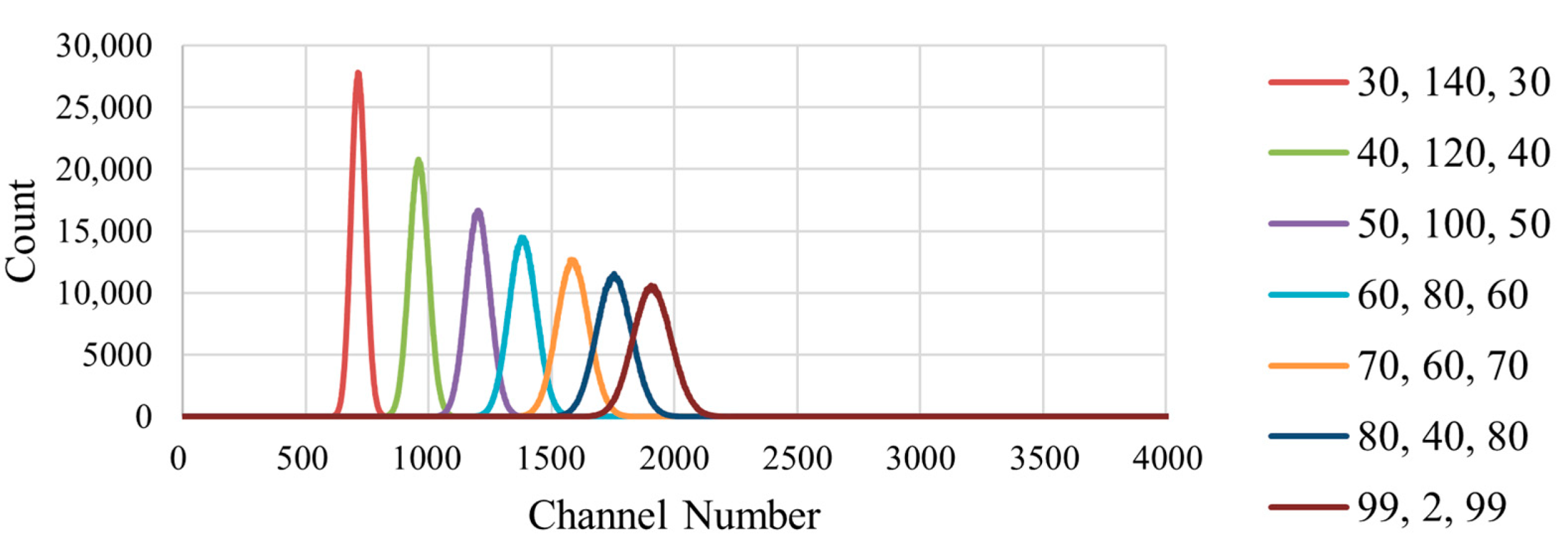
- The Trapezoidal Shaper is a digital algorithm implemented in VHDL to process pulses from SiPM into a suitable spectrum.
- Spectrum Memory is internal FPGA memory that holds the channel data, recording the amount of interactions detected and their corresponding energy levels.
- Python Script: Spectrum Receive and Store listens for spectrum data collected by the FPGA, formatting it into a MySQL database, while a second script running on a remote PC queries the database to obtain the stored spectrum data.
- The MySQL Database: Spectrum Table database holds every spectrum taken at a set rate (every 1.34 s), allowing a record to be kept and accessed wirelessly at a later point.
- With an End User Computer, an end user can access the database and retrieve the spectra data via a private network and then visualize it using a developed python script.
2.1. SiPM Amplifier Design
2.2. SiPM Temperature Compensation
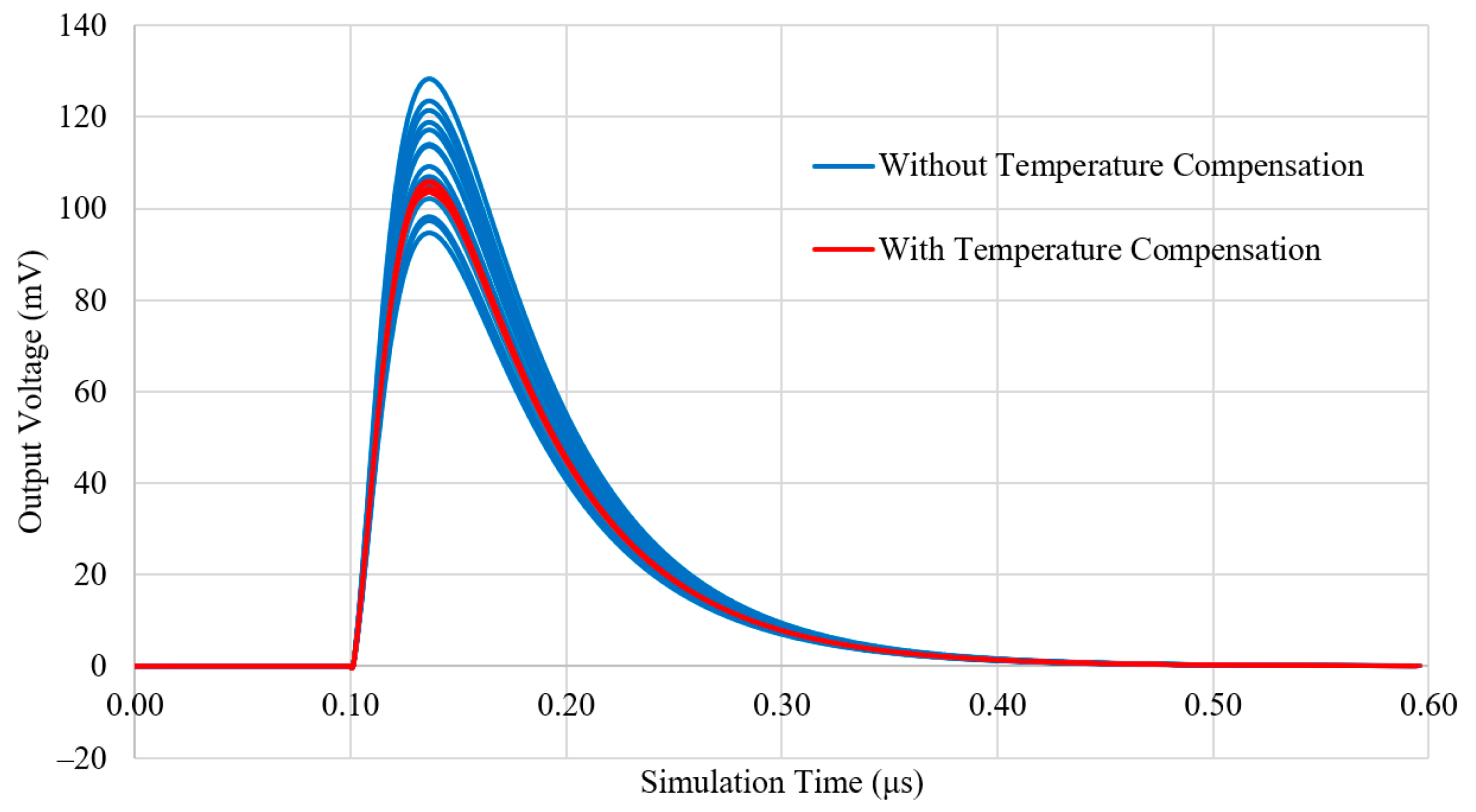
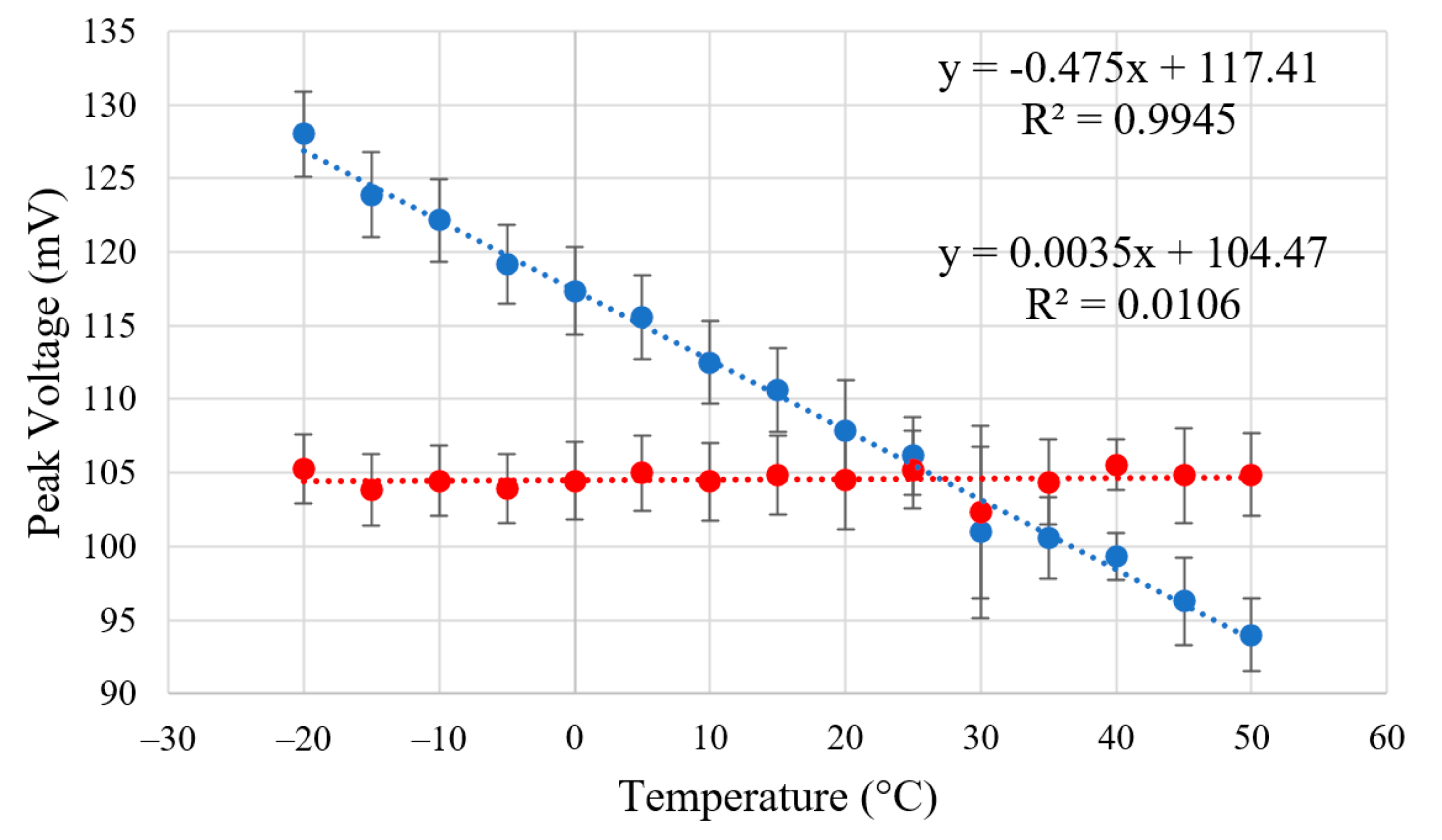
2.3. Temperature Compensation System Simulation
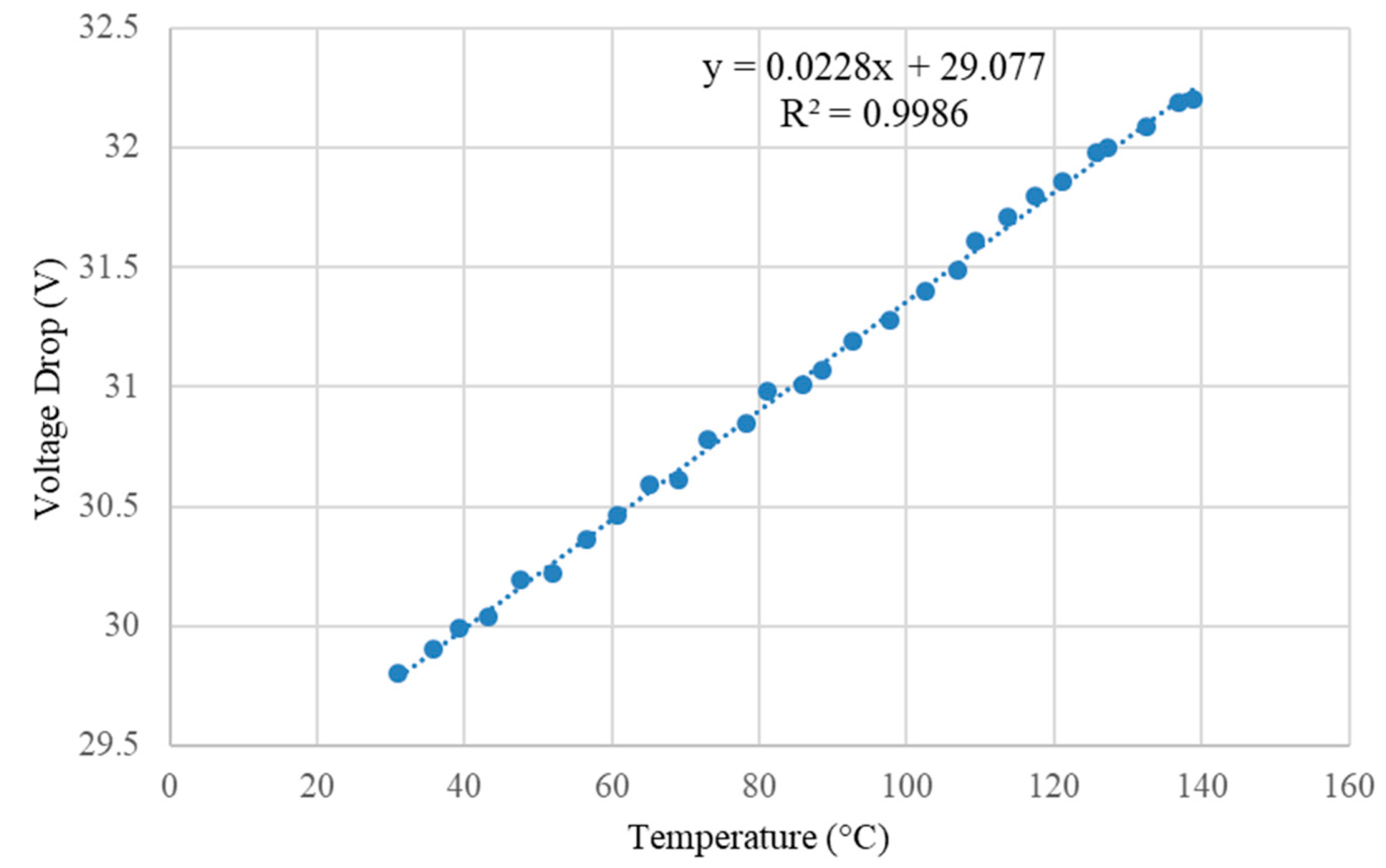
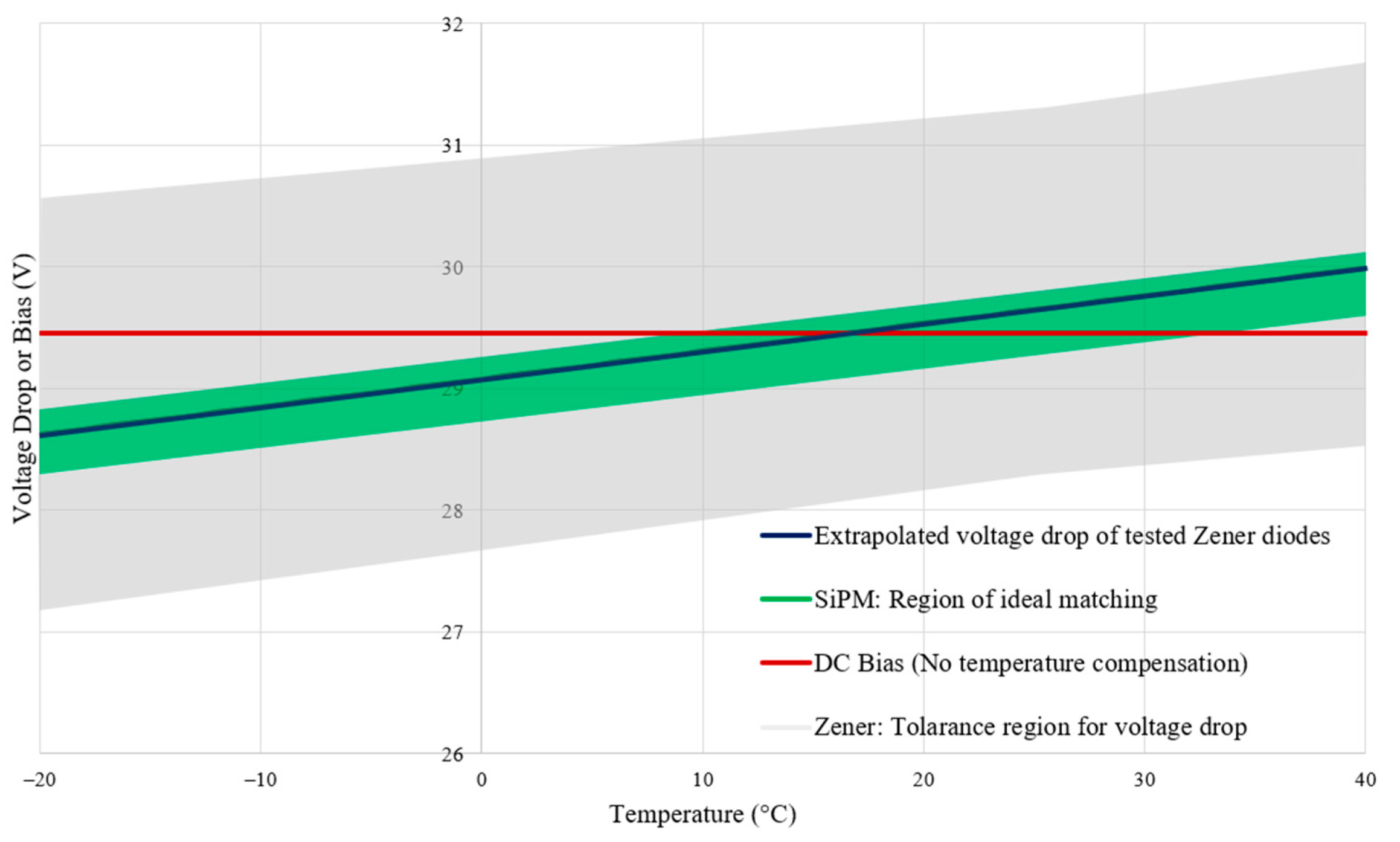
Zener Diode Selection
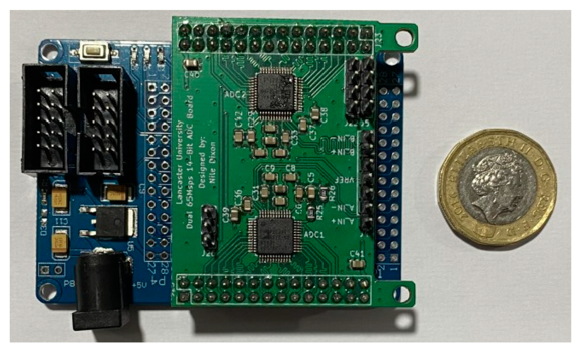
2.4. FPGA and ADC Interconnection Board
2.5. Digital Signal Processing
FPGA Spectrum Accumulation
2.6. Database Design and Implementation
3. Detector Resolution Determination Using LED Pulse Testing
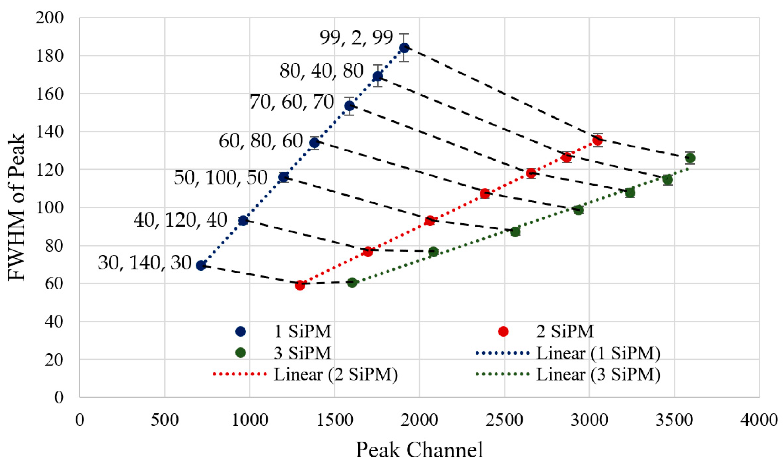
3.1. LED Blinking Experiment Results
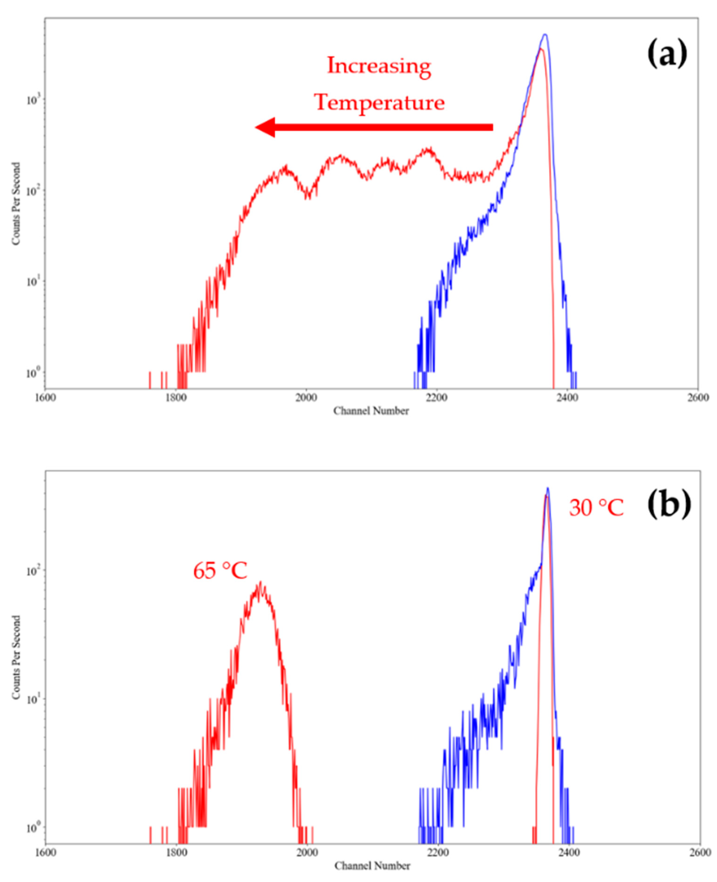
3.2. Temperature Compensation Experiment Results
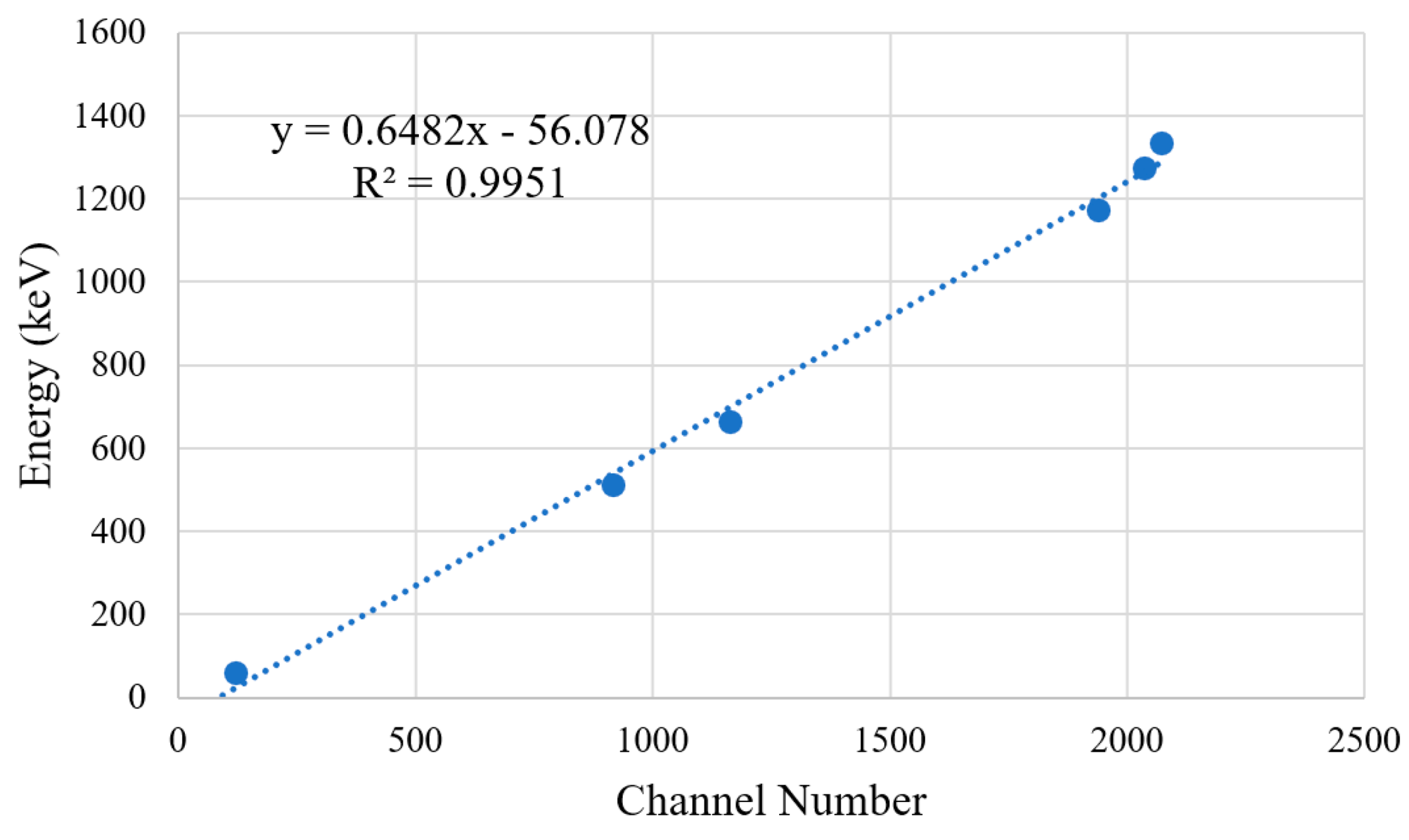
4. Sealed Source Calibration with Temperature Compensation
5. Conclusions
Author Contributions
Funding
Institutional Review Board Statement
Informed Consent Statement
Data Availability Statement
Conflicts of Interest
References
- Otte, A.N.; Garcia, D.; Nguyen, T.; Purushotham, D. Characterization of three high efficiency and blue sensitive silicon photomultipliers. Nucl. Instrum. Methods Phys. Res. Sect. A 2017, 846, 106–125. [Google Scholar] [CrossRef]
- Arriojas, A.; Barros, H.; Walter, J.; Sajó-Bohus, L. FPGA based digital signal processing for high resolution low energy gamma spectrometery. AIP Conf. Proc. 2014, 1607, 65–69. [Google Scholar]
- Becker, E.M.; Farsoni, A.T. Wireless, low-cost, FPGA-based miniature gamma ray spectrometer. Nucl. Instrum. Methods Phys. Res. A 2014, 761, 99–104. [Google Scholar] [CrossRef]
- Lee, P.; Lee, C.S.; Lee, J.H. Development of FPGA-based digital signal processing system for radiation spectroscopy. Radiat. Meas. 2013, 48, 12–17. [Google Scholar] [CrossRef]
- Jordanov, V.T.; Knoll, G.F. Digital synthesis of pulse shapes in real time for high resolution radiation spectroscopy. Nucl. Instrum. Methods Phys. Res. Sect. A Accel. Spectrometers Detect. Assoc. Equip. 1994, 345, 337–345. [Google Scholar] [CrossRef]
- Zhang, J.; Qin, X.; Zhao, M.; Chen, X. FPGA implementation of a real-time digital pulse processing analysis for radiation detectors. Appl. Radiat. Isot. 2021, 176, 109900. [Google Scholar] [CrossRef] [PubMed]
- Jones, H.; Maley, S.; Mousaei, M.; Kohanbash, D.; Whittaker, W.; Teza, J.; Zhang, A.; Jog, N.; Whittaker, W. A Robot for Nondestructive Assay of Holdup Deposits in Gaseous Diffusion Piping. In Proceedings of the WM2019 Conference, Phoenix, AZ, USA, 3–7 March 2019. [Google Scholar]
- International Research Institute for Nuclear Decommissioning. Robots- Various robots that support and take the place of human beings in decommissioning works at Fukushima Daiichi Nuclear Power Station. July 2017. Available online: https://www.jaif.or.jp/IAEA2017/img/IRID_robots2017_eng.pdf (accessed on 18 November 2022).
- Elísio, S.; Joyce, M.J.; Graham, J.; Greenkalgh, B. An advanced blind-tube monitoring instrument to improve the characterization of subsurface radioactive plumes. EPJ Web Conf. 2021, 253, 08005. [Google Scholar] [CrossRef]
- BRIGHTSPEC. Topaz-SiPM. January 2020. Available online: https://www.brightspec.be/brightspec/downloads/Topaz-SiPM_Spec_V1.03.pdf (accessed on 2 September 2022).
- Marques, L.; Vale, A.; Vaz, P. State-of-the-Art Mobile Radiation Detection Systems for Different Scenarios. Sensors 2021, 21, 1051. [Google Scholar] [CrossRef] [PubMed]
- Urban, M.; Nentvich, O.; Marek, L.; Hudec, R.; Sieger, L. Timepix3: Temperature Influence on Radiation Energy Measurement with Si Sensor. Sensors 2023, 23, 2201. [Google Scholar] [CrossRef] [PubMed]
- Onsemi. C-SERIES SIPM: Silicon Photomultiplier Sensors, C-Series (SiPM). Available online: https://www.onsemi.com/products/sensors/photodetectors-sipm-spad/silicon-photomultipliers-sipm/c-series-sipm (accessed on 20 June 2022).
- Kuznetsov, E. Temperature-compensated silicon photomultiplier. Nucl. Instrum. Methods Phys. Res. Sect. A Accel. Spectrometers Detect. Assoc. Equip. 2018, 912, 226–230. [Google Scholar] [CrossRef]
- Licciulli, F.; Marzocca, C. An Active Compensation System for the Temperature Dependence of SiPM Gain. IEEE Trans. Nucl. Sci. 2015, 62, 228–235. [Google Scholar] [CrossRef]
- McGee, K.D. Silicon Photomultiplier Modeling of CsI(Tl) with Front End Electronics using a Monte Carlo Model. Master’s Thesis, Oregon State University, Corvallis, OR, USA, 2019. [Google Scholar]
- Villa, F.; Zou, Y.; Mora, A.D.; Tosi, A.; Zappa, F. SPICE Electrical Models and Simulations of Silicon Photomultipliers. IEEE Trans. Nucl. Sci. 2015, 62, 1950–1960. [Google Scholar] [CrossRef]
- ON Semiconductor. Zener Voltage Regulators: 500 mW SOD−523, Standard Tolerance Series. November 2020. Available online: https://www.mouser.co.uk/datasheet/2/308/MM5Z2V4T1_D-1551523.pdf (accessed on 17 August 2022).
- ON Semiconductor. Zener Voltage Regulators: 300 mW SOD−323 Surface Mount Tight Tolerance Portfolio. December 2015. Available online: https://www.mouser.co.uk/datasheet/2/308/MM3Z2V4ST1_D-1101657.pdf (accessed on 17 August 2022).
- Analog Devices. AD9244. Available online: https://www.analog.com/en/products/ad9244.html#product-overview (accessed on 20 June 2022).
- Jordanov, V.T.; Knoll, G.F.; Hhuber, A.C.; Pantazis, J.A. Digital techniques for real-time pulse shaping in radiation measurements. Nucl. Instrum. Methods Phys. Res. Sect. A-Accel. Spectrometers Detect. Assoc. Equip. 1994, 353, 261–264. [Google Scholar] [CrossRef]
- Altera. Overview: Using the ModelSim Software with the Quartus II Software; Altera: San Jose, CA, USA, 2002; Available online: https://www.slac.stanford.edu/grp/md/ecae/Overview_Using_ModelSim_with_Quartus_II.html (accessed on 18 August 2022).
- Lavelle, C.M.; Shanks, W.; Chiang, C.; Nichols, M.; Osborne, J., Jr.; Herschelman, A.; Brown, B.; Cho, M. Approaches for single channel large area silicon photomultiplier array readout. Am. Inst. Phys. Adv. 2019, 9, 3. [Google Scholar] [CrossRef]
- Advatech. NaI(Tl) Scintillators—Encapsulated. Advatech. Available online: https://www.advatech-uk.co.uk/nai_tl_scint_encap.html (accessed on 20 June 2022).
- WWW Table of Radioactive Isotopes, Gamma Energy Search A = 60. Available online: http://nucleardata.nuclear.lu.se/toi/Gamma.asp?sql=&A1=60&A2=60&Z=27 (accessed on 30 March 2022).
- WWW Table of Radioactive Isotopes, Gamma Energy Search A = 137. Available online: http://nucleardata.nuclear.lu.se/toi/Gamma.asp?sql=&A1=137&A2=137&Z=55 (accessed on 30 March 2022).
- WWW Table of Radioactive Isotopes, Gamma Energy Search A = 22. Available online: http://nucleardata.nuclear.lu.se/toi/Gamma.asp?sql=&A1=22&A2=22&Z=11 (accessed on 30 March 2022).
- Akkurt, I.; Gunoglu, K.; Arda, S.S. Detection Efficiency of NaI(Tl) Detector in 511-1332 keV Energy Range. Sci. Interact. Nucl. Install. 2014, 2014, 186798. [Google Scholar] [CrossRef]
- WWW Table of Radioactive Isotopes, Gamma Energy Search A = 241. Available online: http://nucleardata.nuclear.lu.se/toi/Gamma.asp?sql=&A1=241&A2=241&Z=95 (accessed on 30 March 2022).
- El-Gamal, H.; Negm, H.; Hasabelnaby, M. Detection efficiency of NaI(Tl) detector based on the fabricated calibration of HPGe detector. J. Radiat. Res. Appl. Sci. 2019, 12, 360–366. [Google Scholar] [CrossRef]


| Specification | SiPM (with 5 V Overvoltage) | Zener Diode 5.6 V | Zener Diode 24.2 V | Zener Diodes Combined |
|---|---|---|---|---|
| Min Voltage Drop (V) | 29.2 | 5.49 | 22.8 | 28.29 |
| Max Voltage Drop (V) | 29.7 | 5.73 | 25.6 | 31.33 |
| Min Temperature coefficient (mV/°C) | 21.5 | −2 | 18.4 | 16.4 |
| Max Temperature coefficient (mV/°C) | 21.5 | 2.5 | 22 | 24.5 |
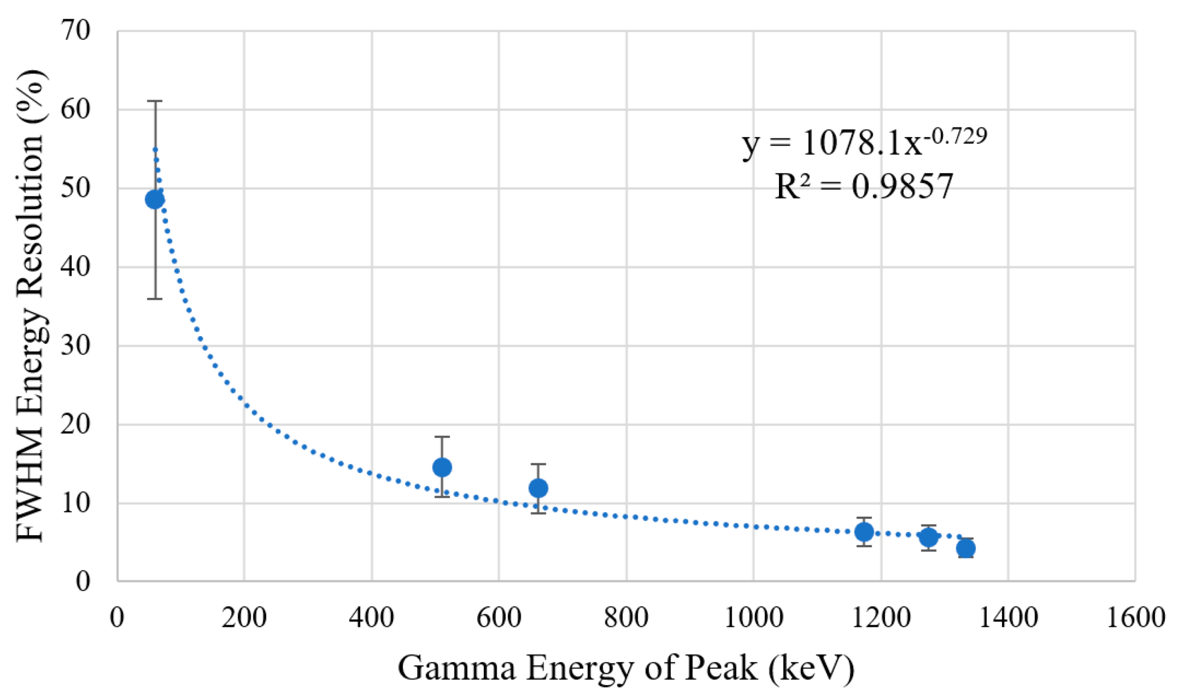
| Isotope | CPS | Collection Time (h) | Feature | Peak Channel (3σ) | Energy (keV) | Resolution (%) (3σ) | FWHM (keV) (3σ) |
|---|---|---|---|---|---|---|---|
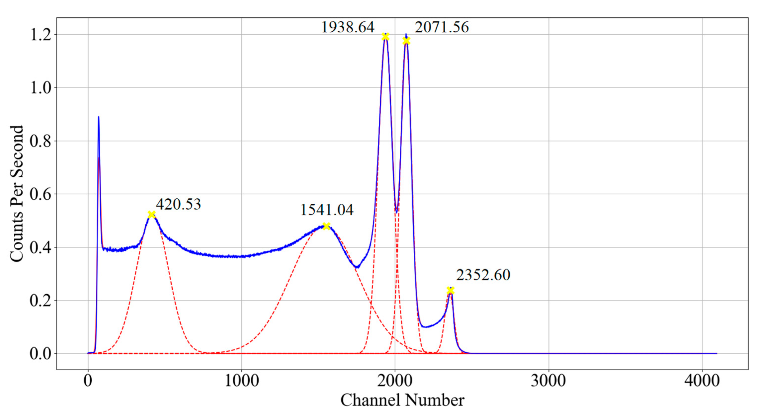
| Co-60 | 1002.85 | 19.76 | Photopeak | 1938.64 ± 3.35 | 1173.24 | 6.30 ± 1.82 | 73.89 ± 21.30 |
| Photopeak | 2071.56 ± 2.23 | 1332.50 | 4.27 ± 1.16 | 56.86 ± 15.47 | |||
| Compton edge | 1541.04 ± 132.30 | - | - | - | |||
| Backscatter | 420.53 ± 21.70 | - | - | - | |||
| Cs-137 | 3614.40 | 9.45 | Photopeak | 1164.38 ± 0.78 | 661.66 | 11.82 ± 3.07 | 78.18 ± 20.29 |
| Backscatter | 371.88 ± 6.26 | - | - | - | |||
| Na-22 | 237.53 | 9.90 | Photopeak | 918.13 ± 2.39 | 511.00 | 14.52 ± 3.82 | 74.19 ± 19.53 |
| Photopeak | 2035.70 ± 4.88 | 1274.53 | 5.57 ± 1.55 | 71.01 ± 19.78 | |||
| Am-241 | 3572.21 | 12.82 | Photopeak | 123.60 ± 0.19 | 59.54 | 48.54 ± 12.58 | 28.90 ± 7.49 |
| Photopeak | 71.53 ± 3.15 | 26.34 | - | - |
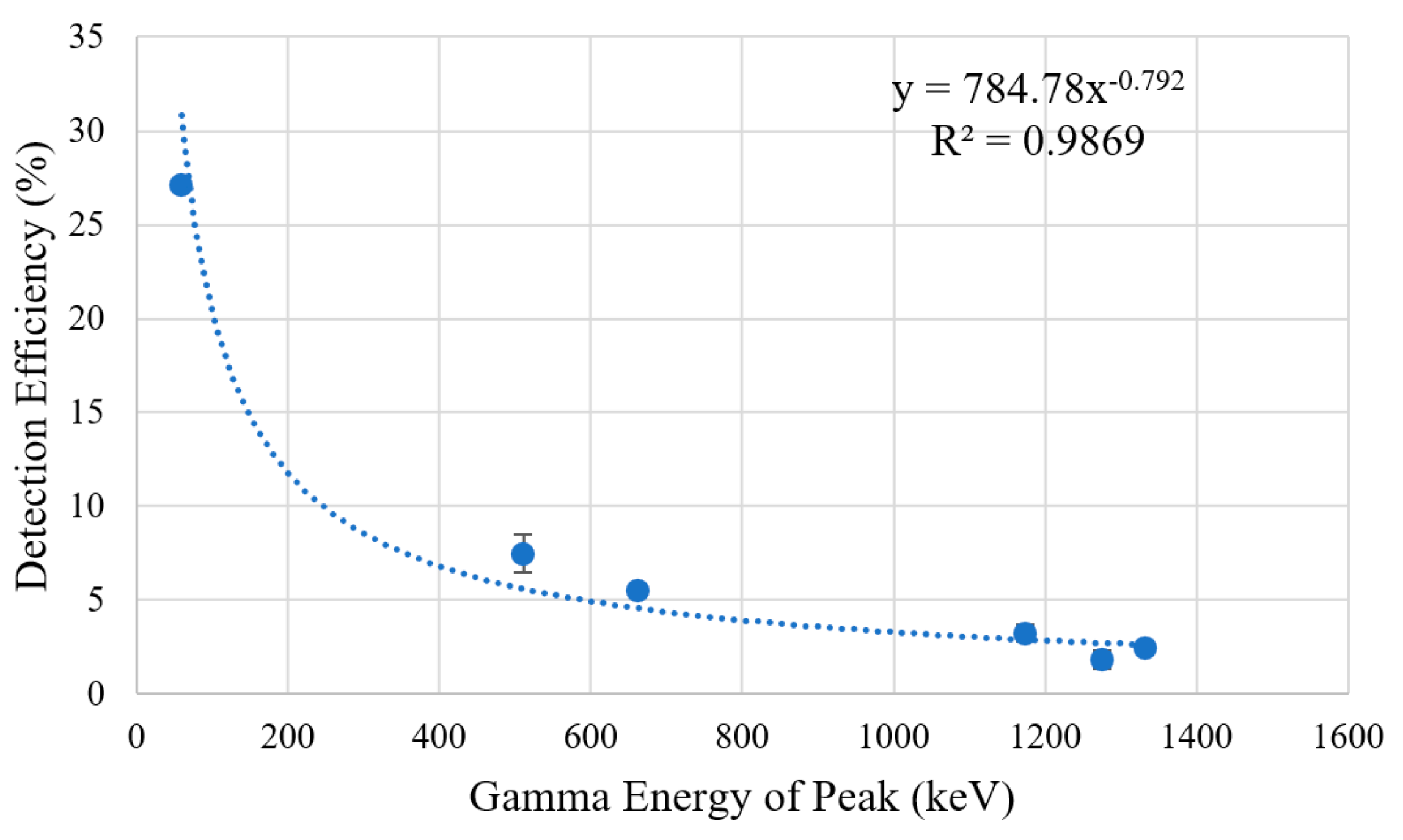
| Specification | Fitted Gamma Energy (keV) | Decay Branching Ratio | Detected Count Rate (CPS) (3σ) | Detection Efficiency (%) (3σ) |
|---|---|---|---|---|
| Co-60 | 1173.24 | 1.00 | 144.79 ± 20.00 | 3.25 ± 0.45 |
| 1332.50 | 1.00 | 110.18 ± 11.15 | 2.47 ± 0.25 | |
| Cs-137 | 661.66 | 0.85 | 1269.48 ± 30.90 | 5.48 ± 0.11 |
| Na-22 | 511.00 | 1.81 | 81.50 ± 6.08 | 7.48 ± 1.01 |
| 1274.53 | 1.00 | 17.06 ± 2.80 | 1.84 ± 0.47 | |
| Am-241 | 59.54 | 0.36 [29] | 3268.31 ± 45.20 | 27.09 ± 0.13 |
Disclaimer/Publisher’s Note: The statements, opinions and data contained in all publications are solely those of the individual author(s) and contributor(s) and not of MDPI and/or the editor(s). MDPI and/or the editor(s) disclaim responsibility for any injury to people or property resulting from any ideas, methods, instructions or products referred to in the content. |
© 2023 by the authors. Licensee MDPI, Basel, Switzerland. This article is an open access article distributed under the terms and conditions of the Creative Commons Attribution (CC BY) license (https://creativecommons.org/licenses/by/4.0/).
Share and Cite
Dixon, N.E.J.; Monk, S.D.; Graham, J.; Cheneler, D. Compact Back-End Electronics with Temperature Compensation and Efficient Data Management for In Situ SiPM-Based Radiation Detection. Sensors 2023, 23, 4053. https://doi.org/10.3390/s23084053
Dixon NEJ, Monk SD, Graham J, Cheneler D. Compact Back-End Electronics with Temperature Compensation and Efficient Data Management for In Situ SiPM-Based Radiation Detection. Sensors. 2023; 23(8):4053. https://doi.org/10.3390/s23084053
Chicago/Turabian StyleDixon, Nile E. J., Stephen D. Monk, James Graham, and David Cheneler. 2023. "Compact Back-End Electronics with Temperature Compensation and Efficient Data Management for In Situ SiPM-Based Radiation Detection" Sensors 23, no. 8: 4053. https://doi.org/10.3390/s23084053
APA StyleDixon, N. E. J., Monk, S. D., Graham, J., & Cheneler, D. (2023). Compact Back-End Electronics with Temperature Compensation and Efficient Data Management for In Situ SiPM-Based Radiation Detection. Sensors, 23(8), 4053. https://doi.org/10.3390/s23084053