
Fabrication of Ultra-Sharp Tips by Dynamic Chemical Etching Process for Scanning Near-Field Microwave Microscopy

 ,
,  , ,
, ,  ,
,  ,
,  and
and 
Abstract
1. Introduction
2. Materials and Methods
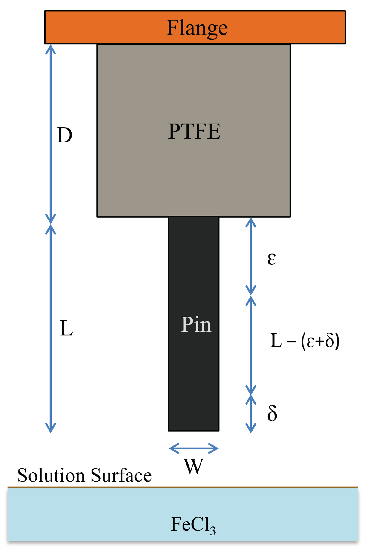
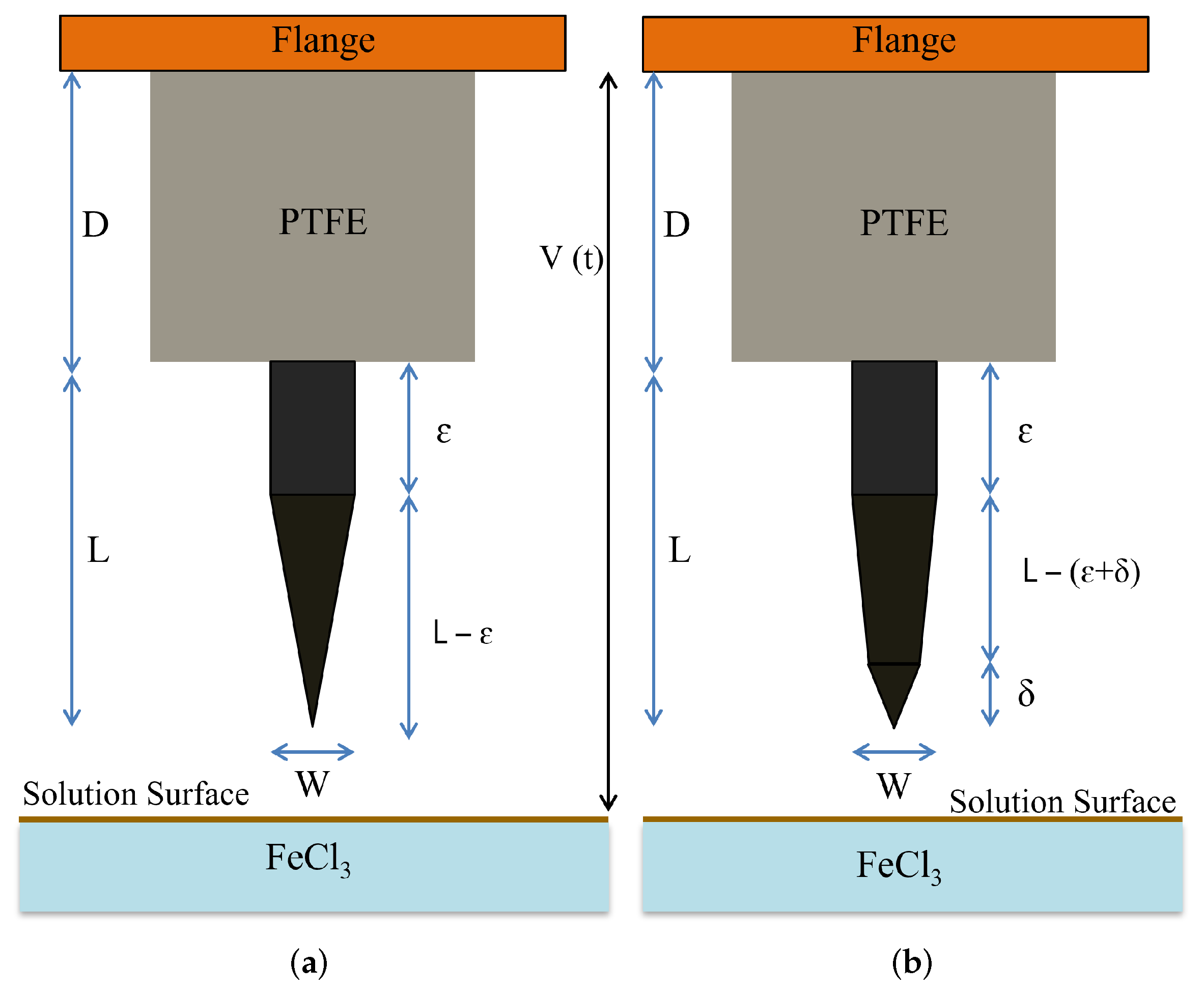
2.1. Chemical Etching Setup
2.2. Chemical Etching Process
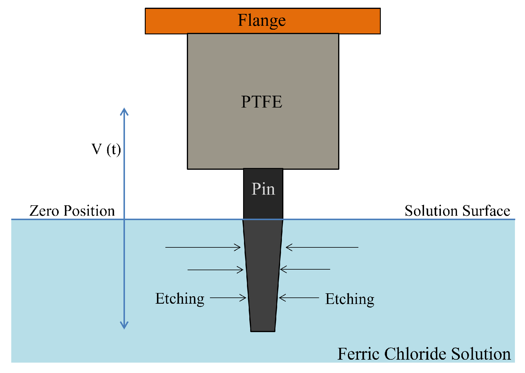
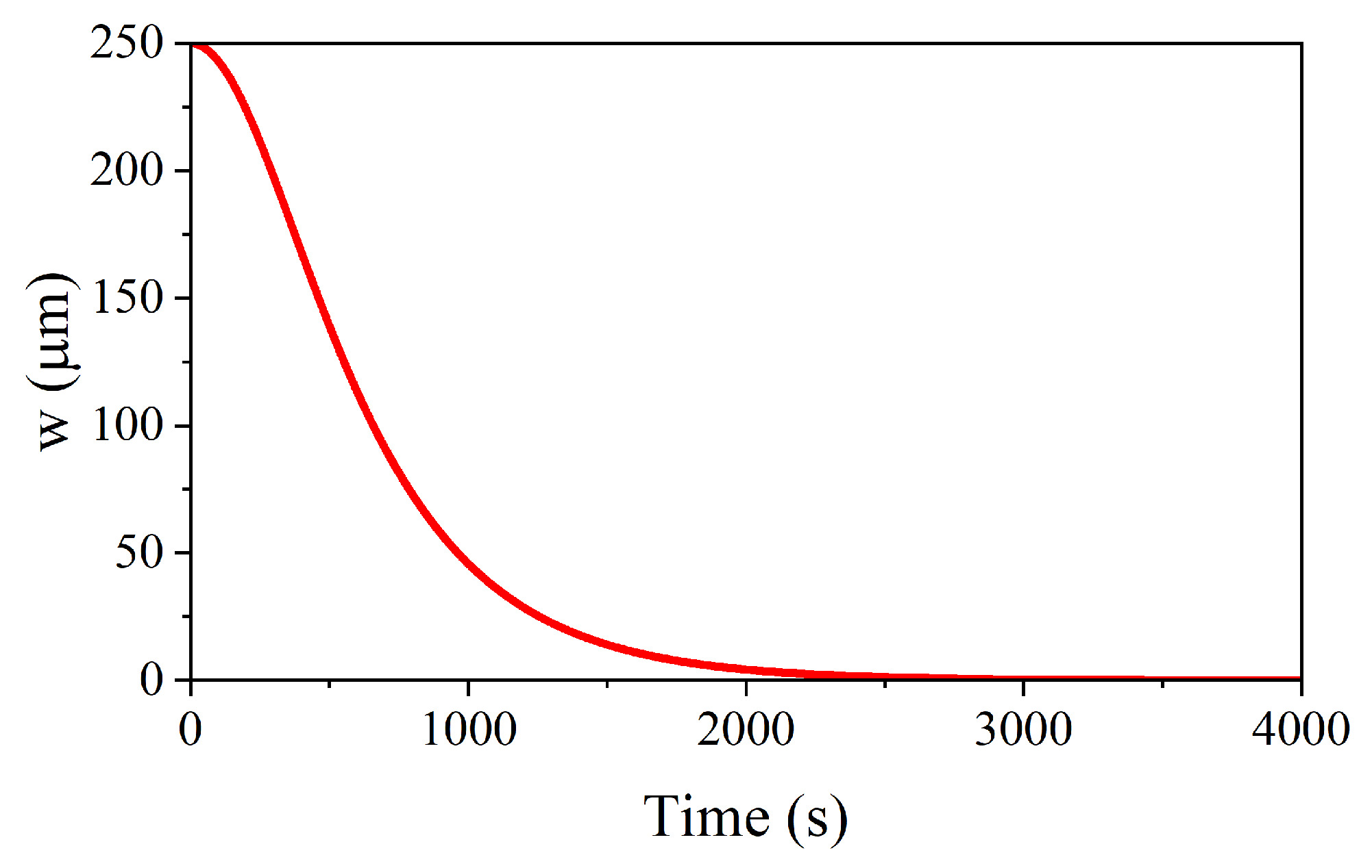
2.3. Tip Formation Dynamics
3. Results and Discussion
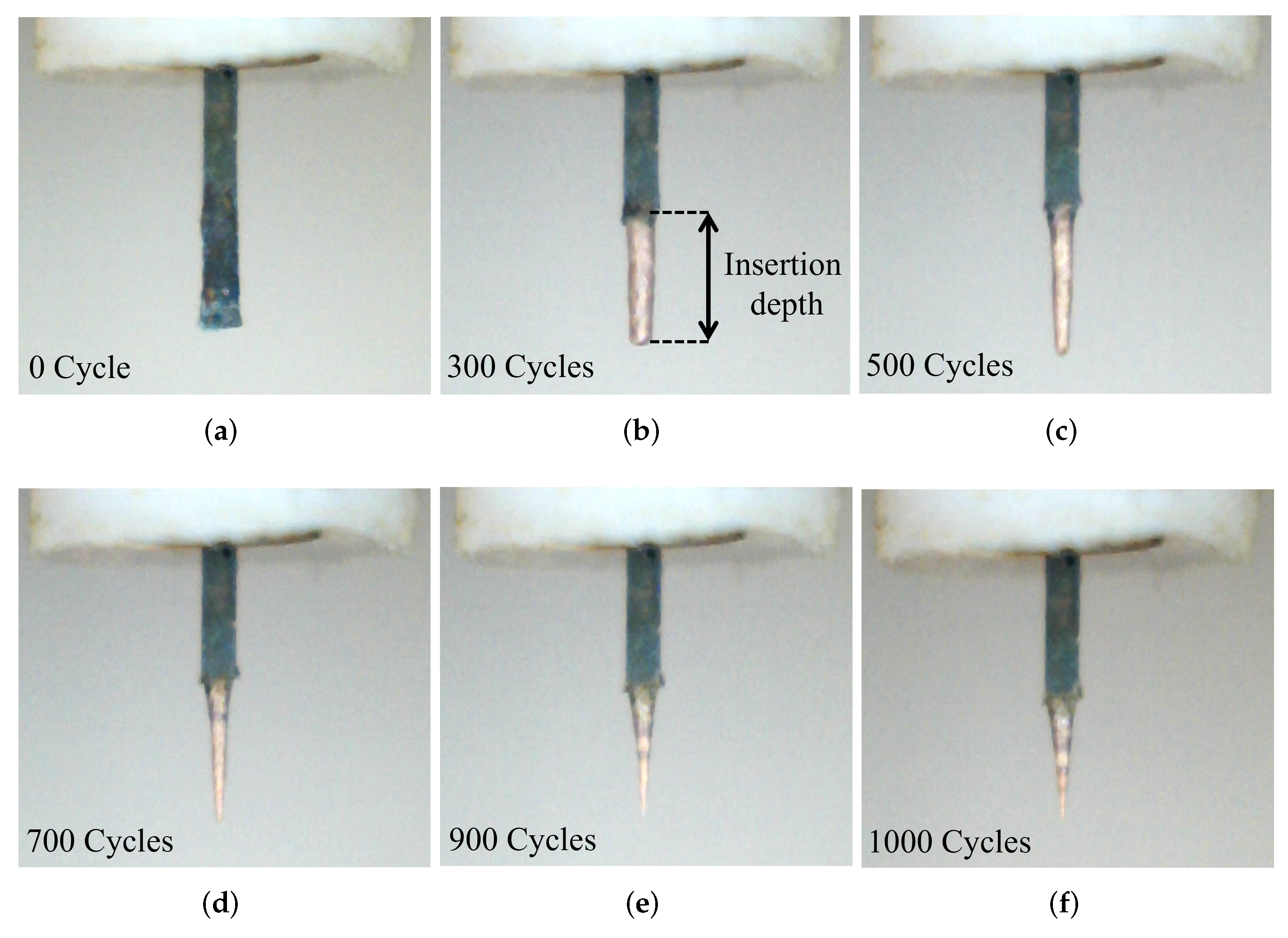
3.1. Dynamic Etching
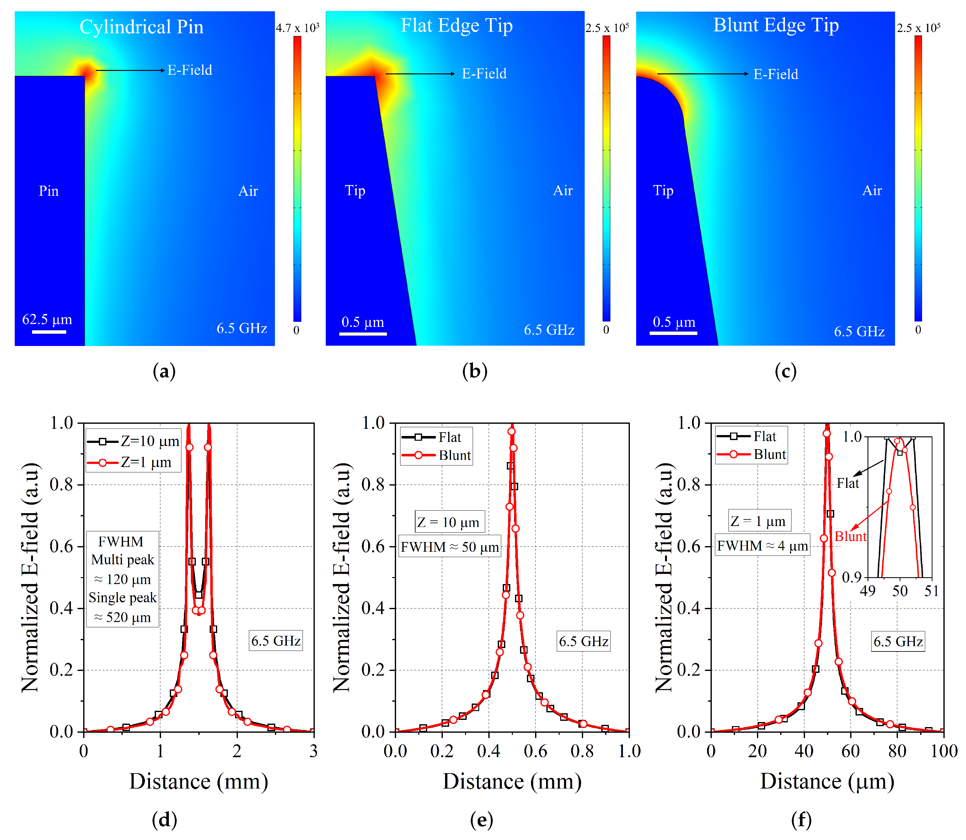
3.2. Near-Field Analysis
3.3. SNMM Imaging Analysis
4. Conclusions
Author Contributions
Funding
Institutional Review Board Statement
Informed Consent Statement
Data Availability Statement
Acknowledgments
Conflicts of Interest
References
- Imtiaz, A.; Anlage, S.M. Effect of tip geometry on contrast and spatial resolution of the near-field microwave microscope. J. Appl. Phys. 2006, 100, 044304. [Google Scholar] [CrossRef]
- Siegel, P.H. Microwaves Are Everywhere: “SMM: Nano-Microwaves”. IEEE J. Microwaves 2021, 1, 838–852. [Google Scholar] [CrossRef]
- Synge, E.H. XXXVIII. A suggested method for extending microscopic resolution into the ultra-microscopic region. Philos. Mag. J. Sci. 1928, 6, 356–362. [Google Scholar] [CrossRef]
- Ash, E.; Nicholls, G. Super-resolution Aperture Scanning Microscope. Nature 1972, 237, 510–512. [Google Scholar] [CrossRef] [PubMed]
- Anlage, S.M.; Talanov, V.V.; Schwartz, A.R. Principles of Near-Field Microwave Microscopy. In Scanning Probe Microscopy: Electrical and Electromechanical Phenomena at the Nanoscale; Kalinin, S., Gruverman, A., Eds.; Springer: New York, NY, USA, 2007; pp. 215–253. [Google Scholar]
- Gao, C.; Xiang, X.D. Quantitative microwave near-field microscopy of dielectric properties. Rev. Sci. Instrum. 1998, 69, 3846–3851. [Google Scholar]
- Michalas, L.; Brinciotti, E.; Lucibello, A.; Gramse, G.; Joseph, C.H.; Kienberger, F.; Proietti, E.; Marcelli, R. De-embedding techniques for nanoscale characterization of semiconductors by scanning microwave microscopy. Microelectron. Eng. 2016, 159, 64–69. [Google Scholar] [CrossRef]
- Brinciotti, E.; Gramse, G.; Hommel, S.; Schweinboeck, T.; Altes, A.; Fenner, M.A.; Smoliner, J.; Kasper, M.; Badino, G.; Tuca, S.S.; et al. Probing resistivity and doping concentration of semiconductors at the nanoscale using scanning microwave microscopy. Nanoscale 2015, 7, 14715–14722. [Google Scholar] [CrossRef]
- Fabi, G.; Jin, X.; Pavoni, E.; Joseph, C.H.; Di Donato, A.; Mencarelli, D.; Wang, X.; Al Hadi, R.; Morini, A.; Hwang, J.C.M.; et al. Quantitative Characterization of Platinum Diselenide Electrical Conductivity With an Inverted Scanning Microwave Microscope. IEEE Trans. Microw. Theory Tech. 2021, 69, 3348–3359. [Google Scholar] [CrossRef]
- Wu, D.; Li, W.; Rai, A.; Wu, X.; Movva, H.C.P.; Yogeesh, M.N.; Chu, Z.; Banerjee, S.K.; Akinwande, D.; Lai, K. Visualization of Local Conductance in MoS2/WSe2 Heterostructure Transistors. Nano Lett. 2019, 19, 1976–1981. [Google Scholar] [CrossRef]
- Tselev, A.; Yu, P.; Cao, Y.; Dedon, L.R.; Martin, L.W.; Kalinin, S.V.; Maksymovych, P. Microwave a.c. conductivity of domain walls in ferroelectric thin films. Nat. Commun. 2016, 7, 11630. [Google Scholar]
- Wu, X.; Du, K.; Zheng, L.; Wu, D.; Cheong, S.W.; Lai, K. Microwave conductivity of ferroelectric domains and domain walls in a hexagonal rare-earth ferrite. Phys. Rev. B 2018, 98, 081409. [Google Scholar] [CrossRef]
- Joseph, C.H.; Gramse, G.; Proietti, E.; Sardi, G.M.; Morley, G.W.; Kienberger, F.; Bartolucci, G.; Marcelli, R. Local Characterization of Ferromagnetic Resonance in Bulk and Patterned Magnetic Materials Using Scanning Microwave Microscopy. IEEE Trans. Instrum. Meas. 2022, 71, 1–11. [Google Scholar] [CrossRef]
- Joseph, C.H.; Luzi, F.; Azman, S.N.A.; Forcellese, P.; Pavoni, E.; Fabi, G.; Mencarelli, D.; Gentili, S.; Pierantoni, L.; Morini, A.; et al. Nanoscale Characterization of Graphene Oxide-Based Epoxy Nanocomposite Using Inverted Scanning Microwave Microscopy. Sensors 2022, 22, 9608. [Google Scholar] [CrossRef]
- Biagi, M.C.; Fabregas, R.; Gramse, G.; Van Der Hofstadt, M.; Juárez, A.; Kienberger, F.; Fumagalli, L.; Gomila, G. Nanoscale Electric Permittivity of Single Bacterial Cells at Gigahertz Frequencies by Scanning Microwave Microscopy. ACS Nano 2016, 10, 280–288. [Google Scholar] [CrossRef]
- Farina, M.; Hwang, J.C.M. Scanning Microwave Microscopy for Biological Applications: Introducing the State of the Art and Inverted SMM. IEEE Microw. Mag. 2020, 21, 52–59. [Google Scholar] [CrossRef]
- Jin, X.; Farina, M.; Wang, X.; Fabi, G.; Cheng, X.; Hwang, J.C.M. Quantitative Scanning Microwave Microscopy of the Evolution of a Live Biological Cell in a Physiological Buffer. IEEE Trans. Microw. Theory Tech. 2019, 67, 5438–5445. [Google Scholar] [CrossRef]
- Gramse, G.; Brinciotti, E.; Lucibello, A.; Patil, S.B.; Kasper, M.; Rankl, C.; Giridharagopal, R.; Hinterdorfer, P.; Marcelli, R.; Kienberger, F. Quantitative sub-surface and non-contact imaging using scanning microwave microscopy. Nanotechnology 2015, 26, 135701. [Google Scholar] [CrossRef]
- Plassard, C.; Bourillot, E.; Rossignol, J.; Lacroute, Y.; Lepleux, E.; Pacheco, L.; Lesniewska, E. Detection of defects buried in metallic samples by scanning microwave microscopy. Phys. Rev. B 2011, 83, 121409. [Google Scholar] [CrossRef]
- Frait, Z. The use of high-frequency modulation in studying ferromagnetic resonance. Czech J. Phys. 1959, 9, 403–404. [Google Scholar] [CrossRef]
- Soohoo, R.F. A Microwave Magnetic Microscope. J. Appl. Phys. 1962, 33, 1276–1277. [Google Scholar] [CrossRef]
- Rosner, B.T.; van der Weide, D.W. High-frequency near-field microscopy. Rev. Sci. Instrum. 2002, 73, 2505–2525. [Google Scholar] [CrossRef]
- Lee, Y.; Alu, A.; Zhang, J.X. Efficient apertureless scanning probes using patterned plasmonic surfaces. Opt. Express 2011, 19, 25990–25999. [Google Scholar] [CrossRef] [PubMed]
- Wei, T.; Xiang, X.; Wallace-Freedman, W.G.; Schultz, P.G. Scanning tip microwave near-field microscope. Appl. Phys. Lett. 1996, 68, 3506–3508. [Google Scholar] [CrossRef]
- Tabib-Azar, M.; Su, D.P.; Pohar, A.; LeClair, S.R.; Ponchak, G. 0.4 μm spatial resolution with 1 GHz (λ=30 cm) evanescent microwave probe. Rev. Sci. Instrum. 1999, 70, 1725–1729. [Google Scholar] [CrossRef]
- Tabib-Azar, M.; Shoemaker, N.S.; Harris, S. Non-destructive characterization of materials by evanescent microwaves. Meas. Sci. Technol. 1993, 4, 583. [Google Scholar] [CrossRef]
- Steinhauer, D.E.; Vlahacos, C.P.; Dutta, S.K.; Feenstra, B.J.; Wellstood, F.C.; Anlage, S.M. Quantitative imaging of sheet resistance with a scanning near-field microwave microscope. Appl. Phys. Lett. 1998, 72, 861–863. [Google Scholar] [CrossRef]
- Lai, K.; Kundhikanjana, W.; Kelly, M.A.; Shen, Z.X. Nanoscale microwave microscopy using shielded cantilever probes. Appl. Nanosci. 2011, 1, 13–18. [Google Scholar] [CrossRef]
- Wang, Y.; Bettermann, A.D.; van der Weide, D.W. Process for scanning near-field microwave microscope probes with integrated ultratall coaxial tips. J. Vac. Sci. Technol. B Microelectron. Nanometer Struct. Process. Meas. Phenom. 2007, 25, 813–816. [Google Scholar] [CrossRef]
- Weber, J.C.; Blanchard, P.T.; Sanders, A.W.; Imtiaz, A.; Wallis, T.M.; Coakley, K.J.; Bertness, K.A.; Kabos, P.; Sanford, N.A.; Bright, V.M. Gallium nitride nanowire probe for near-field scanning microwave microscopy. Appl. Phys. Lett. 2014, 104, 023113. [Google Scholar] [CrossRef]
- Grant, J.P.; Clarke, R.N.; Symm, G.T.; Spyrou, N.M. A critical study of the open-ended coaxial line sensor technique for RF and microwave complex permittivity measurements. J. Phys. E Sci. Instrum. 1989, 22, 757. [Google Scholar] [CrossRef]
- Joseph, C.H.; Subramanian, V. Novel Phase Based Feedback Control for Constant Height Mode Operation in Scanning Near-Field Microwave Microscopy. In Electromagnetic Nondestructive Evaluation XXII; Tamburrino, A., Deng, Y., Chakrapani, S., Eds.; Studies in Applied Electromagnetics and Mechanics; IOS Press: Bristol, UK, 2019; Volume 44, pp. 20–25. [Google Scholar]
- Lucibello, A.; Sardi, G.M.; Capoccia, G.; Proietti, E.; Marcelli, R.; Kasper, M.; Gramse, G.; Kienberger, F. A broadband toolbox for scanning microwave microscopy transmission measurements. Rev. Sci. Instrum. 2016, 87, 053701. [Google Scholar] [CrossRef]
- SMA Series. Available online: http://www.sricomworld.in/smaseries.html (accessed on 8 February 2023).
- Wang, Z.; Che, J.; Ye, C. Application of ferric chloride both as oxidant and complexant to enhance the dissolution of metallic copper. Hydrometallurgy 2010, 105, 69–74. [Google Scholar] [CrossRef]
- Alimov, M.M.; Kornev, K.G. Meniscus on a shaped fibre: Singularities and hodograph formulation. Proc. R. Soc. Math. Phys. Eng. Sci. 2014, 470, 20140113. [Google Scholar] [CrossRef]
- Tang, Y.; Cheng, S. The meniscus on the outside of a circular cylinder: From microscopic to macroscopic scales. J. Colloid Interface Sci. 2019, 533, 401–408. [Google Scholar] [CrossRef] [PubMed]
- Somlyai-Sipos, L.; Baumli, P. Wettability of Metals by Water. Metals 2022, 12, 1274. [Google Scholar] [CrossRef]
- Golosovsky, M.; Maniv, E.; Davidov, D.; Frenkel, A. Near-field of a scanning aperture microwave probe: A 3-D finite element analysis. IEEE Trans. Instrum. Meas. 2002, 51, 1090–1096. [Google Scholar] [CrossRef]
- Steinhauer, D.E.; Vlahacos, C.P.; Wellstood, F.C.; Anlage, S.M.; Canedy, C.; Ramesh, R.; Stanishevsky, A.; Melngailis, J. Imaging of microwave permittivity, tunability, and damage recovery in (Ba,Sr)TiO3 thin films. Appl. Phys. Lett. 1999, 75, 3180–3182. [Google Scholar] [CrossRef]
- Capoccia, G.; Sardi, G.M.; Marcelli, R.; Proietti, E. Near field microwave microscopy for MEMS and micro-electronic device characterization. In Proceedings of the 2018 Symposium on Design, Test, Integration and Packaging of MEMS and MOEMS (DTIP), Rome, Italy, 22–25 May 2018; pp. 1–4. [Google Scholar]
- Sardi, G.M.; Lucibello, A.; Kasper, M.; Gramse, G.; Proietti, E.; Kienberger, F.; Marcelli, R. Optimization of the imaging response of scanning microwave microscopy measurements. Appl. Phys. Lett. 2015, 107, 033107. [Google Scholar] [CrossRef]


| Velocity (mm/sec) | Total no. of Cycles | Time for 100 Cycles (min) | Insertion Depth (mm) |
|---|---|---|---|
| 1 | 1000 | 10:59 | 0.5 |
| 2 | 1000 | 4:59 | 0.8 |
| 4 | 1000 | 3:42 | 0.7 |
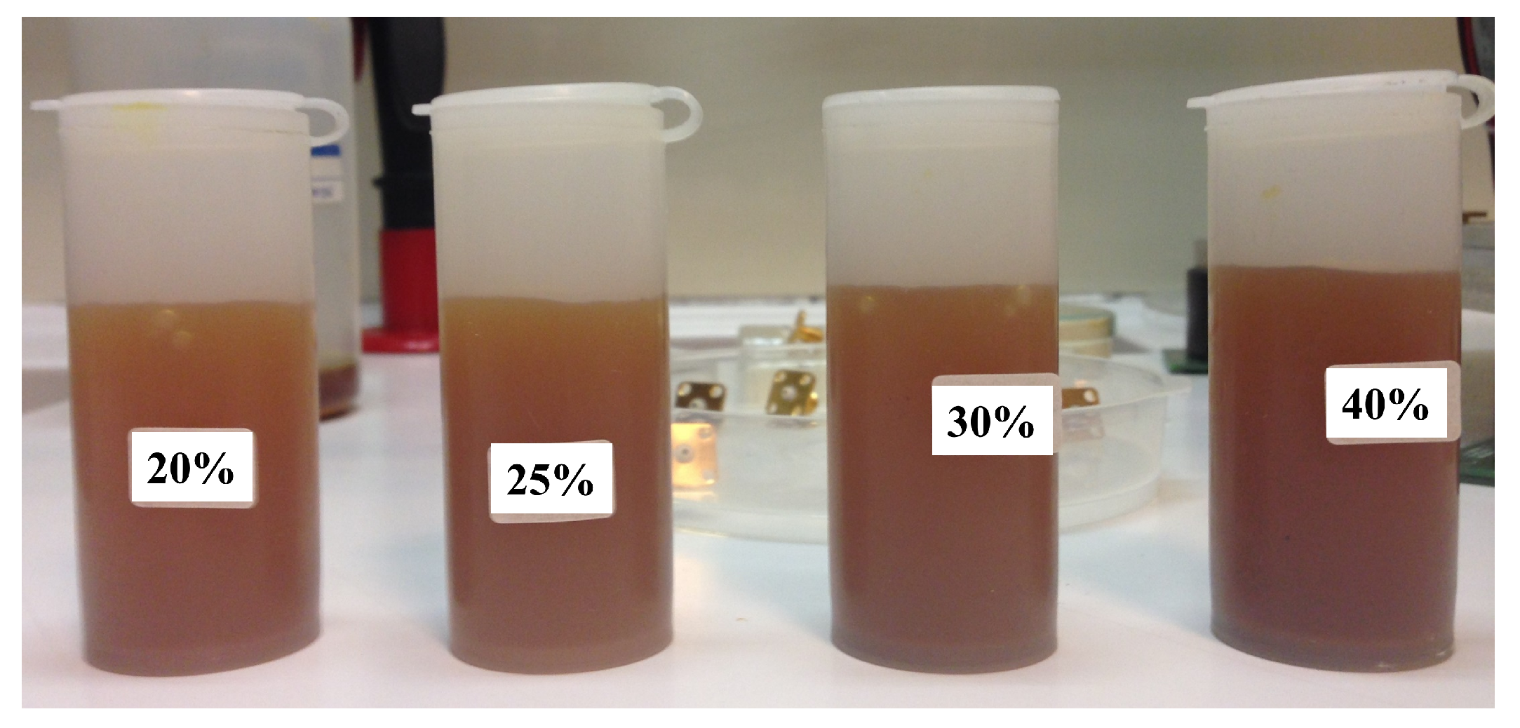
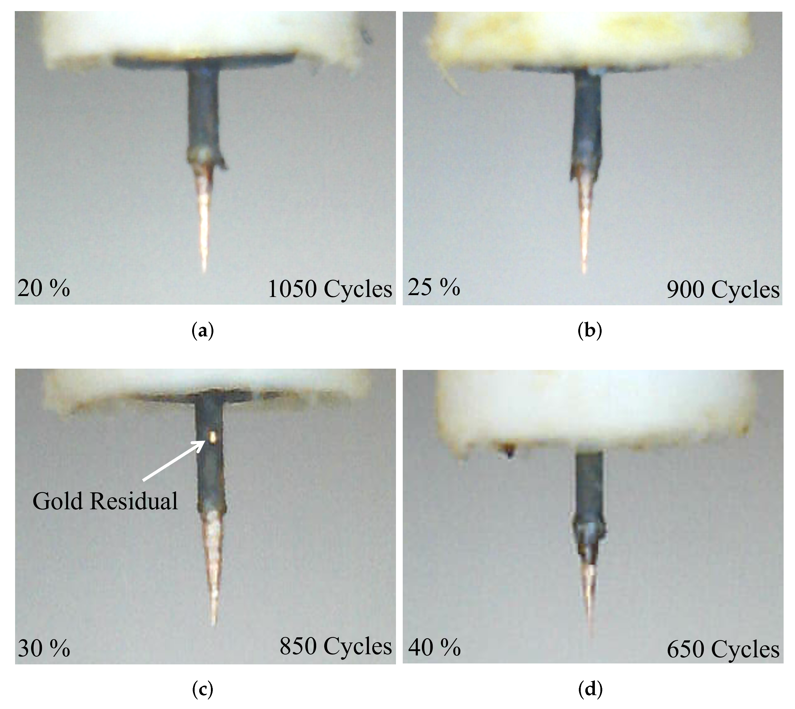
| Concentration (%) | Total no. of Cycles | Velocity (mm/sec) | Time for 100 Cycles (min) | Insertion Depth (mm) |
|---|---|---|---|---|
| 40 | 650 | 2 | 4:59 | 0.7 |
| 30 | 850 | 2 | 4:59 | 0.7 |
| 20 | 900 | 2 | 4:59 | 0.7 |
| 10 | 1050 | 2 | 4:59 | 0.7 |
Disclaimer/Publisher’s Note: The statements, opinions and data contained in all publications are solely those of the individual author(s) and contributor(s) and not of MDPI and/or the editor(s). MDPI and/or the editor(s) disclaim responsibility for any injury to people or property resulting from any ideas, methods, instructions or products referred to in the content. |
© 2023 by the authors. Licensee MDPI, Basel, Switzerland. This article is an open access article distributed under the terms and conditions of the Creative Commons Attribution (CC BY) license (https://creativecommons.org/licenses/by/4.0/).
Share and Cite
Joseph, C.H.; Capoccia, G.; Lucibello, A.; Proietti, E.; Sardi, G.M.; Bartolucci, G.; Marcelli, R. Fabrication of Ultra-Sharp Tips by Dynamic Chemical Etching Process for Scanning Near-Field Microwave Microscopy. Sensors 2023, 23, 3360. https://doi.org/10.3390/s23063360
Joseph CH, Capoccia G, Lucibello A, Proietti E, Sardi GM, Bartolucci G, Marcelli R. Fabrication of Ultra-Sharp Tips by Dynamic Chemical Etching Process for Scanning Near-Field Microwave Microscopy. Sensors. 2023; 23(6):3360. https://doi.org/10.3390/s23063360
Chicago/Turabian StyleJoseph, C. H., Giovanni Capoccia, Andrea Lucibello, Emanuela Proietti, Giovanni Maria Sardi, Giancarlo Bartolucci, and Romolo Marcelli. 2023. "Fabrication of Ultra-Sharp Tips by Dynamic Chemical Etching Process for Scanning Near-Field Microwave Microscopy" Sensors 23, no. 6: 3360. https://doi.org/10.3390/s23063360
APA StyleJoseph, C. H., Capoccia, G., Lucibello, A., Proietti, E., Sardi, G. M., Bartolucci, G., & Marcelli, R. (2023). Fabrication of Ultra-Sharp Tips by Dynamic Chemical Etching Process for Scanning Near-Field Microwave Microscopy. Sensors, 23(6), 3360. https://doi.org/10.3390/s23063360