1. Introduction
During the fabrication process of printed circuit boards (PCBs), the presence of fine particles or flaws in copper patterns can cause PCBs to malfunction [
1,
2]. Therefore, defect screening is a crucial step in the semiconductor manufacturing process for PCBs. Defects can be caused by many factors, including materials, techniques, equipment, and processing substrates [
1]. Various inspection systems, such as automated visual inspection (AVI) [
2,
3], X-ray imaging [
4], ultrasonic imaging [
5], and thermal imaging [
6], have been used to detect defects. Advanced AVI systems utilize high-resolution cameras and defect detection algorithms to inspect PCB surfaces at the panel level [
2]. Similar to AVI systems, automatic final vision inspection (AFVI) systems can be used to inspect the surfaces of PCBs at the strip level to detect various types of defects such as cracks, nicks, protrusions, and foreign materials.
Various defect detection algorithms have been utilized in AVI and AFVI systems, such as reference-based [
7], rule-based [
8,
9], and learning-based approaches [
10,
11]. The majority of these algorithms attempt to find similarities between the reference and inspected images. Nadaf and Kolkure used a subtraction algorithm to detect differences from reference images of typical defect regions on PCBs [
7]. The primary purpose of reference-based approaches is to determine precise alignments between the reference and test images [
12]. Oguz et al. introduced a design-rule-based defect detection algorithm for verifying the requirements of the geometric design rules of conductor spacings, trace widths, and land widths for digital binary PCB images [
9]. Benedek proposed a rule-based framework for generating parent–child relationships based on an intensity histogram to detect soldering defects in PCBs [
8].
Recently, the use of learning-based algorithms for defect inspection has increased rapidly. Zhang et al. utilized a support vector machine (SVM) to recognize and classify defect regions by extracting histograms and geometric features from PCB images [
11]. Deep-learning approaches have also been employed to assist in filtering false defect images prior to manual verification [
2]. Deng et al. proposed an automatic real-time defect classification approach based on deep learning to determine real defects in regions of interest in PCBs [
10]. These methods can reduce the burden of manual verification by facilitating the classification of defects. Although deep learning-based defect detection models are expected to alleviate the cost of manual labeling once developed, they require a manual labeling process to supply a significant amount of data for training the model.
Previous studies have employed a transfer-learning approach to reduce the amount of training data [
13,
14]. Miao et al. employed a cost-sensitive Siamese network based on transfer learning to differentiate defects in PCBs [
14]. Imoto et al. developed an automatic defect classification system that employed unreliably labeled data to train a convolutional neural network model to classify multiple defect types [
10]. Although previous studies have proven the feasibility of the deep-learning approach for defect detection, the model performance remains limited by the shortage and incorrect labeling of training data. He et al. proposed a semi-supervised learning (SSL)-based model to detect defect locations in a DeepPCB dataset [
15]. This approach required pairs of defect-free templates and defective test images for comparison. Shi et al. utilized an adversarial SSL method to train only normal PCB samples and detected extremely small, unknown defects during the test [
16]. Although the network can be trained with lesser data for the SSL model, the use of golden template images (i.e., normal images) for training has disadvantages, such as a lack of flexibility for variations (e.g., misalignment and discoloration) and the need to acquire and store numerous reference patterns [
1,
12].
When defect cases are relatively broad and the differences between defect and non-defect cases are small, the chances of false detection by the defect detection algorithms (e.g., golden template images or machine-learning approaches) of the AFVI system remain high. Hence, following the inspection of the AFVI system, human operators verify whether the defects detected by the AFVI system are true or false to reduce the false detection rate. This manual operation incurs high labor costs and is time-consuming. Manual inspection remains a problem owing to the shortage of labor and expertise. In this study, an SSL approach, PCB_SS, is developed. It can detect defects in PCBs from strip-level images acquired using an AFVI system. The PCB_SS model utilizes labeled data and leverages unlabeled data for training with various augmentations. While varying the amount of labeled data, the performance of the PCB SS model was compared to that of a fully supervised approach, PCB FS, which uses only labeled data. Moreover, the accuracies of the PCB_SS and PCB_FS models were evaluated using noisy (incorrectly labeled) training data in an error-resilience test. To compare the performances of the models for defect detection, extreme gradient boosting (XGBoost) and EfficientNet-B5 were chosen for the machine-learning and deep-learning approaches, respectively.
The highlights of this study are as follows:
- (1)
An SSL approach is developed for significantly varying defect cases with small differences from the non-defect cases, where the golden template and machine-learning approaches are less effective.
- (2)
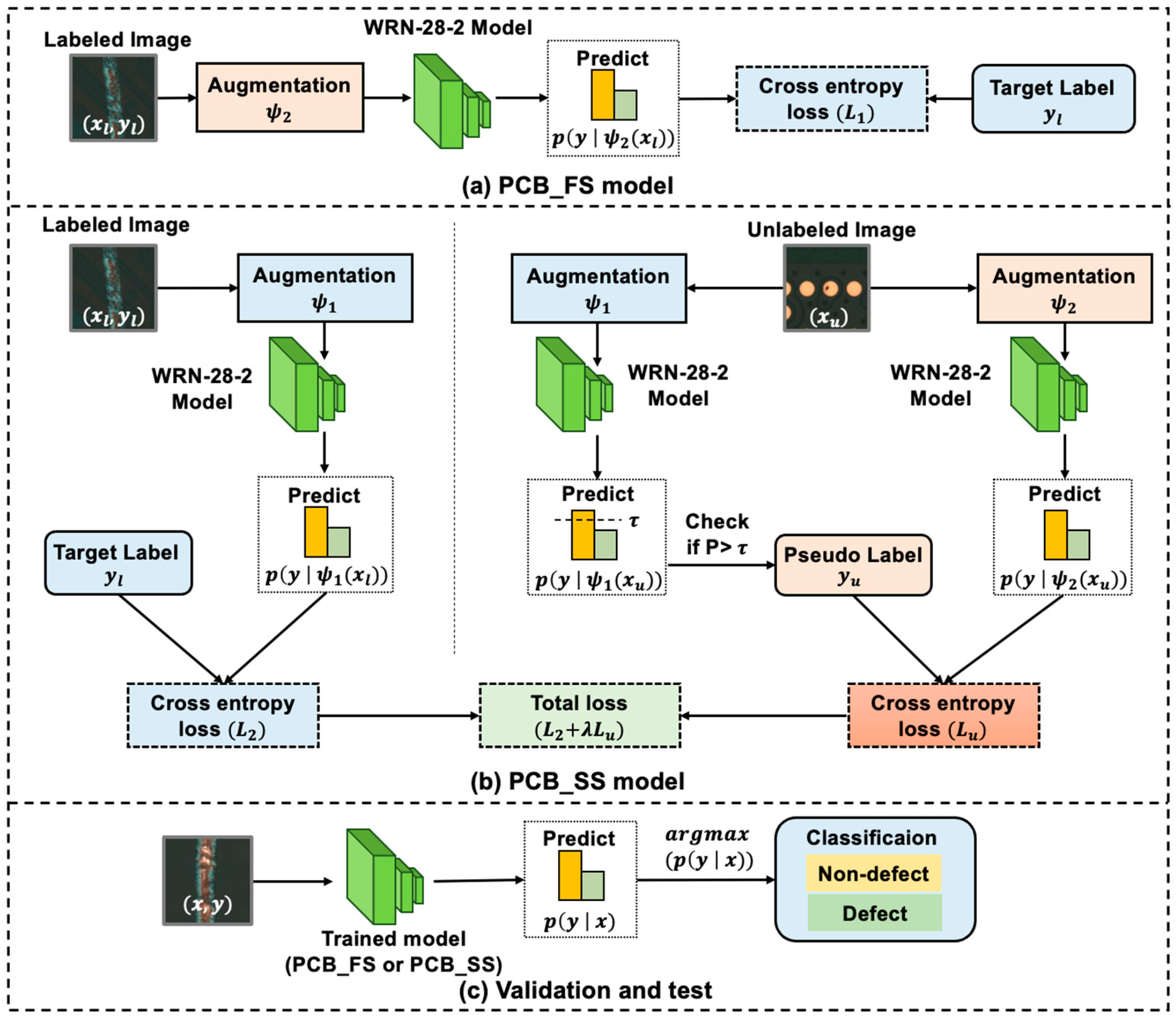
By employing the FixMatch concept with varying augmentations, the PCB_SS model was trained using images classified as defects from the AFVI system with unlabeled and manually labeled target data.
- (3)
An error-resilience test was performed for false detection. The PCB_SS model outperformed PCB_FS for incorrectly labeled data.
- (4)
By alleviating the false defect detection from the AFVI systems, PCB_SS can reduce the burden of manual defect detection, requiring intensive labor with expertise in PCB inspection.
4. Discussion
This study demonstrated the robustness of the PCB_SS model for defect classification when the labeled data were limited or incorrectly labeled for training. The proposed PCB_SS model can benefit from the inspection procedure by reducing the burden of manual inspection. Although the SSL approach for the PCB_SS model was adopted from the FixMatch model [
18], the applications of which are limited to object-specific classification, the defect detection in this study was related to feature-related recognition rather than object detection. Furthermore, optimal augmentations for labeled and unlabeled data were selected to improve the effectiveness of the model in increasing the diversity of data without label changes (
Table 9). In the SSL approach, it is difficult for the model to generate a neighbor connection between the perturbed versions of the unlabeled data and labeled data with no augmentation (
or augmentation
. Thus, the labeled and unlabeled data for the pseudo-label prediction of the PCB_SS model were augmented by augmentation
. Augmentation
, as shown in
Figure 2a, can increase the variation in the dataset for various types, shapes, and sizes of defects. The training process for the labeled data can be accelerated because of the model with different augmented data after each evaluation step [
19]. Labeled data are critical for creating the underlying feature space, and SSL takes advantage of prior knowledge of the domain and data distribution to relate the data and labels to improve the classification performance [
17,
18,
24,
31,
32]. For the PCB_FS model, augmentation
, as shown in
Figure 2b, comprehensively generates diverse variations in the training dataset and reduces the search space of the transformations [
19,
32]. The computational time for inspecting a strip-level PCB image was 164 GFLOPs, which required 25 ms, using the resources utilized in this study.
Table 6 shows a comparison of the proposed model with the machine-learning (XGBoost) and deep-learning (EfficientNet) approaches. The results show that the proposed model is efficient for PCB defect detection, especially when the differences between the defect and non-defect images are small and the defect cases vary widely. Because the percentage of misclassified defect patches from the AFVI system is high (90%, on average), it is crucial to utilize a deep-learning approach to enhance the inspection process to alleviate the false detection of the AFVI system and thus further require manual validation. Based on this comparison, the current backbone model (i.e., WRN-28-2) is superior to EfficientNet. However, various deep-learning models can be selected as the backbone for the future work.
Training the network using unlabeled data and adding unsupervised loss made it possible to generalize the parameters of the PCB_SS model (i.e., overfitting was avoided) (
Figure 5). This generalization of the model can help classify unseen data, which were not previously introduced into the training data, based on the information learned from the unlabeled data. As shown in
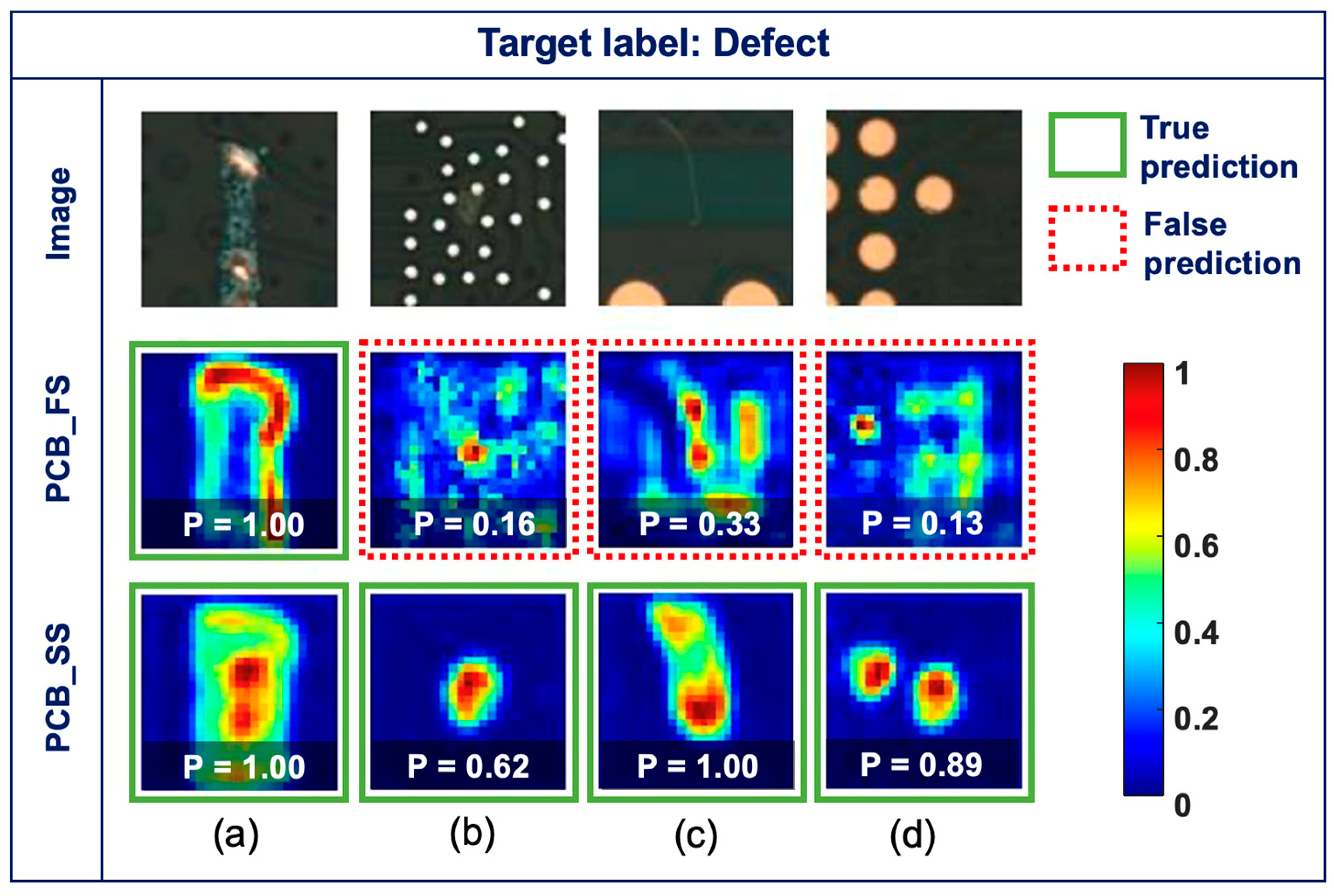
Figure 5, the difference in the validation losses between the PCB_FS and PCB_SS models was higher than the difference in the validation accuracies between the models. This can occur when the model is less certain about the prediction, resulting in a higher loss even though the model predicts correctly. The Grad-CAM maps (
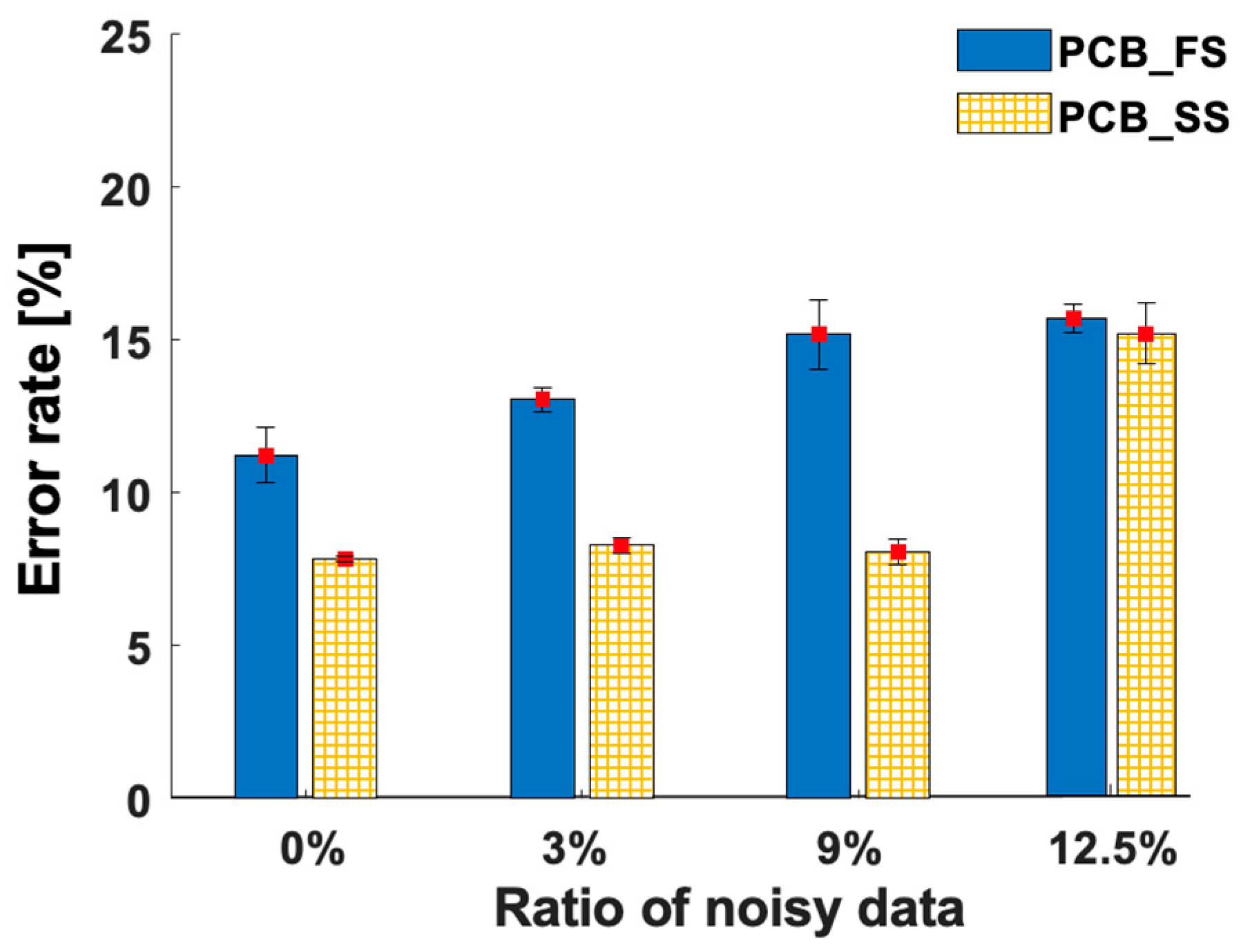
Figure 8) visually confirmed that the model extracted features from the defect regions for decision making. Furthermore, the augmentation process did not affect the decision features, although it modified the training images. In addition, the PCB_SS model can resist noisy data better than the PCB_FS model (
Table 7 and
Figure 7).
In this study, the error rate of the unlabeled data with a probability exceeding the predefined threshold (τ) for the PCB_SS model decreased as the number of labeled data increased from 250 to 4000 (15.94% and 3.95% for Label_250 and Label_4000, respectively). This proves that a larger number of correctly labeled data can provide more guidance for the learning procedure, which also improves the clustering process for unlabeled data. The quality of the pseudo-labels predicted from the unlabeled data is critical for obtaining a high accuracy with the PCB_SS model. Further investigations can be conducted on the dynamic threshold to adaptively select appropriate unlabeled samples to avoid degradation of the overall performance. As wider variations were expected for defect cases than for non-defect cases, the proportions of unlabeled data for defects and non-defects were imbalanced (i.e., more defects than non-defect data), as shown in
Table 1. The results of the confusion matrices (
Figure 6) demonstrated that the reduction in the false prediction of the defect class (42%) between the PCB_FS and PCB_SS models was more significant than that of the non-defect class (10%). Considering that the main objective of inspection is not to miss the defects in PCBs, imbalanced data can improve the classification performance. As demonstrated in the confusion matrix (
Figure 6), the PCB_SS model had fewer false predictions than the PCB_FS model for the test set.
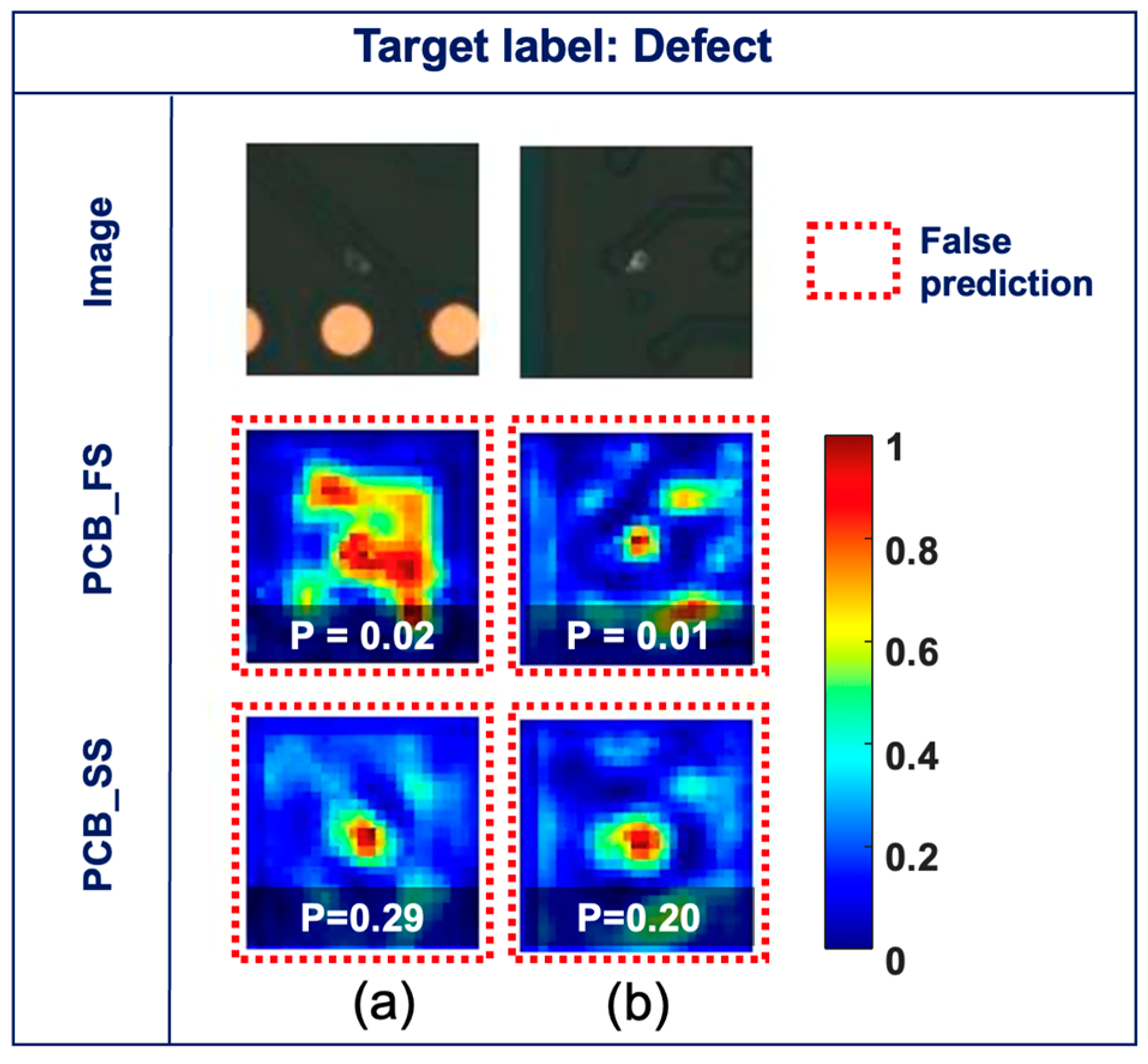
Figure 9 shows the Grad-CAM maps of the two defect images that were misclassified by the PCB_FS and PCB_SS models. Both defects are related to a foreign object (e.g., dust), which is difficult to detect visually. Although the images were misclassified, the Grad-CAM maps showed that the PCB_SS model still concentrated on the defect location. However, the prediction results were also affected by the low activation (approximately 0.3–0.4) of the surrounding regions. Further analysis must be conducted to develop a model that is less affected by the activation of the surrounding region [
33].
The current study had several limitations. The PCB_SS model expects the ROI images to locate defect candidates from the AFVI system. Thus, it is necessary to acquire patch images to apply the current approach to whole PCBs or assembled PCBs (i.e., PCBAs). When new circuit patterns are tested, the proposed model may require further updates by training with additional circuit-pattern images. The new training process can be performed efficiently by utilizing transfer learning from the previous weights of the model. For the best Label_4000 model, the percentage of unlabeled data with a probability higher than the threshold (
) was only 88%. The PCB_SS model requires further improvement by creating close connections between the labeled and unlabeled data [
34].
The results of this study demonstrate that the PCB_SS model performs effectively when a limited number of data are labeled or a portion of them are incorrectly labeled. The proposed model was most effective when the defect cases varied significantly with small changes from the non-defect cases. Combining this method with the AFVI system is expected to significantly minimize the need for manual inspection for false detections and potentially reduce the cost incurred in the PCB manufacturing process.


