

A 0.5 MP, 3D-Stacked, Voltage-Domain Global Shutter Image Sensor with NIR QE Enhancement, Event Detection Modes, and 90 dB Dynamic Range
Abstract
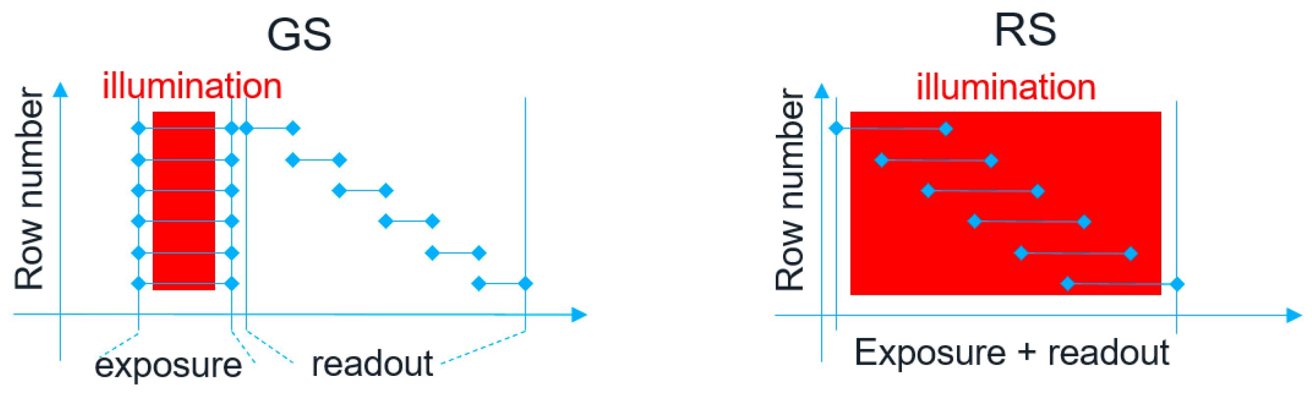
:1. Introduction
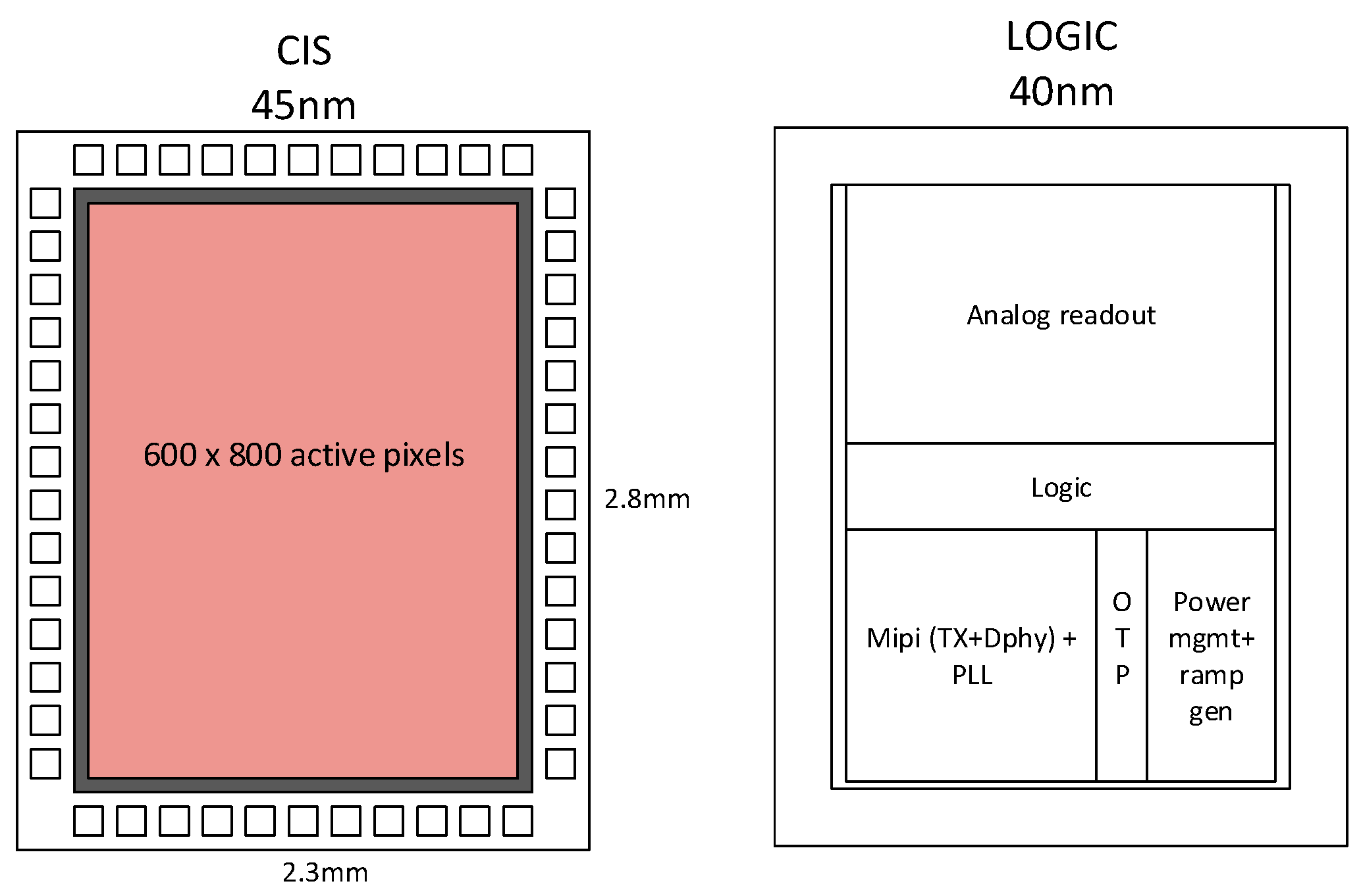
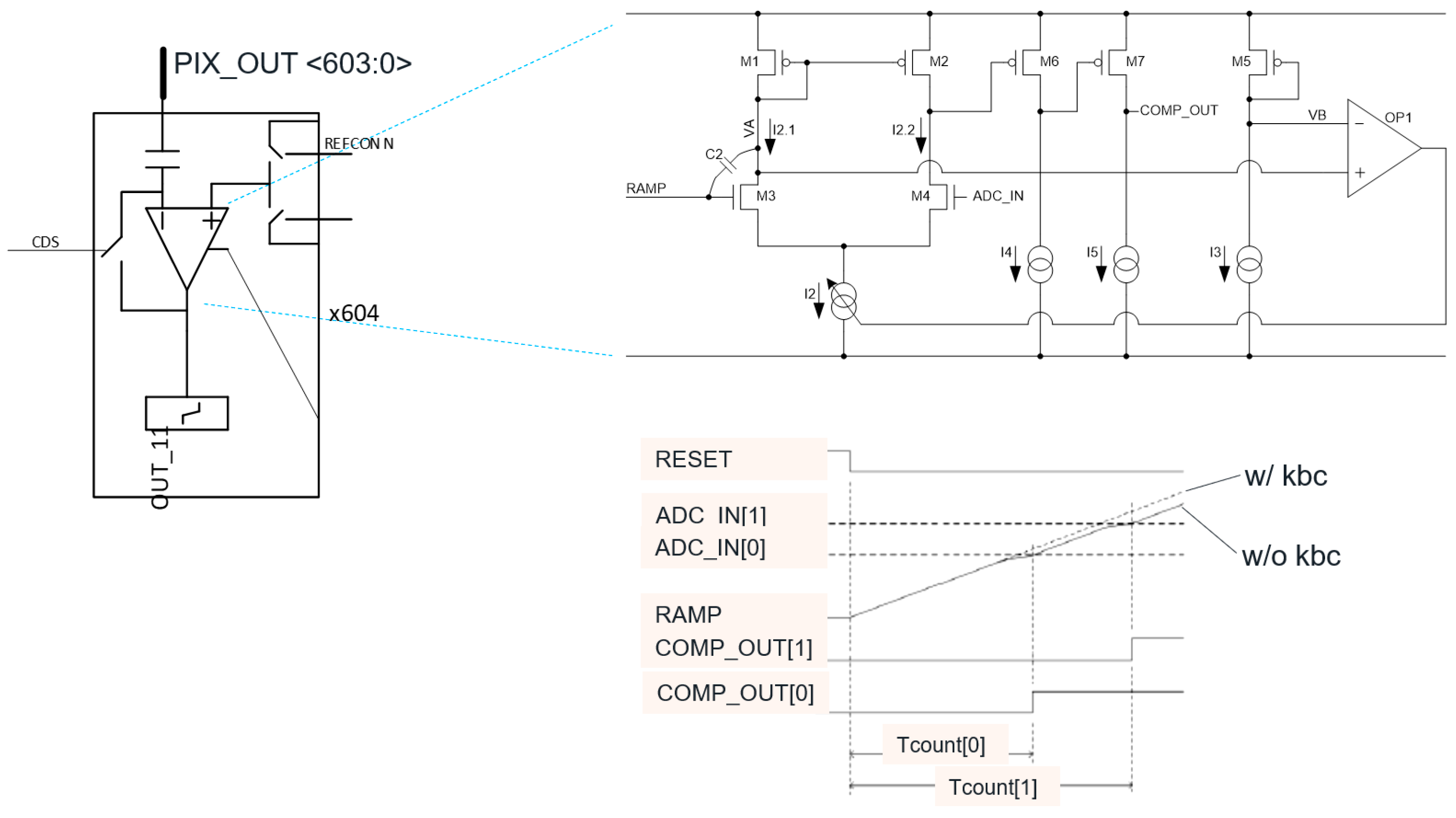
2. Sensor Architecture
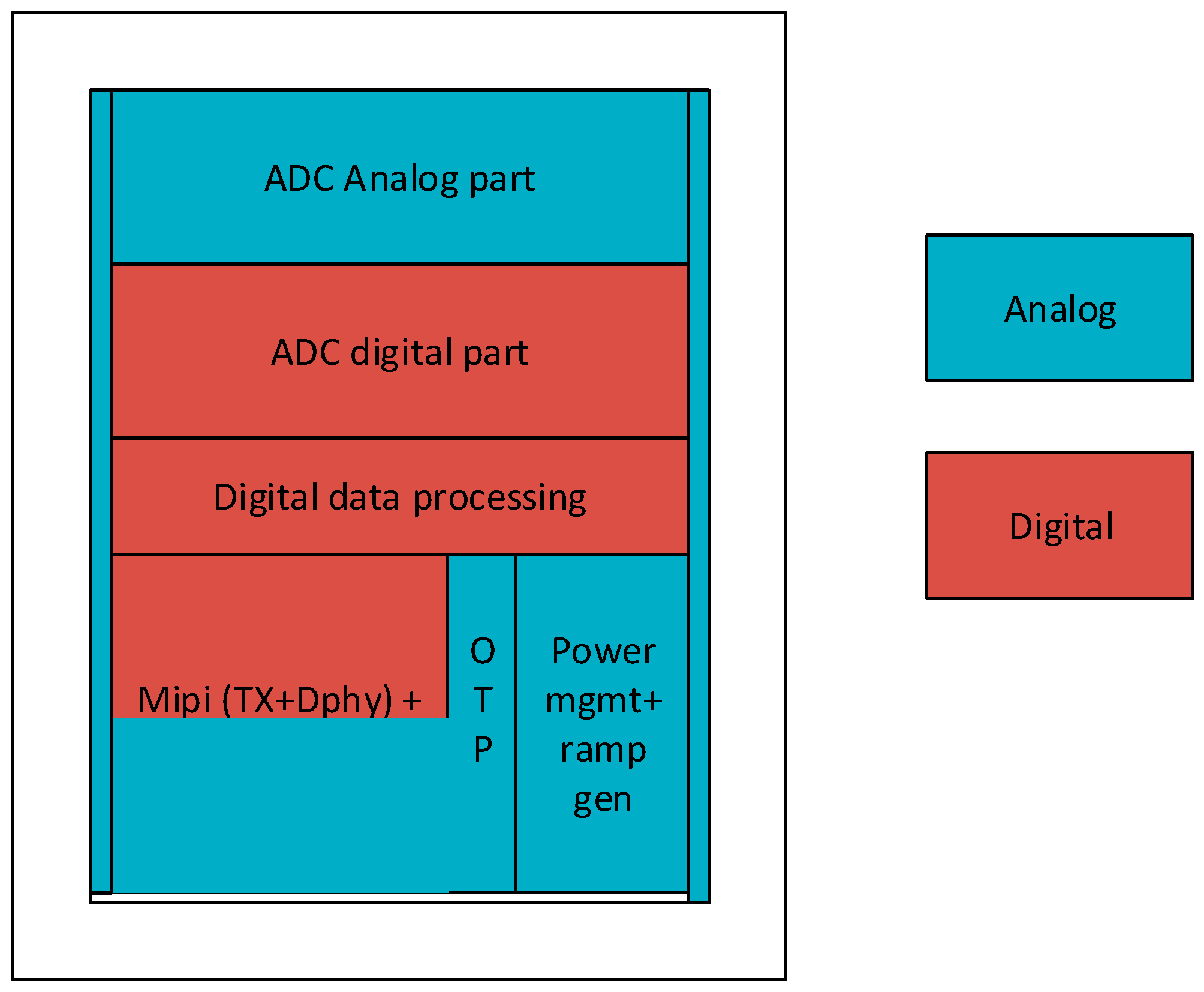
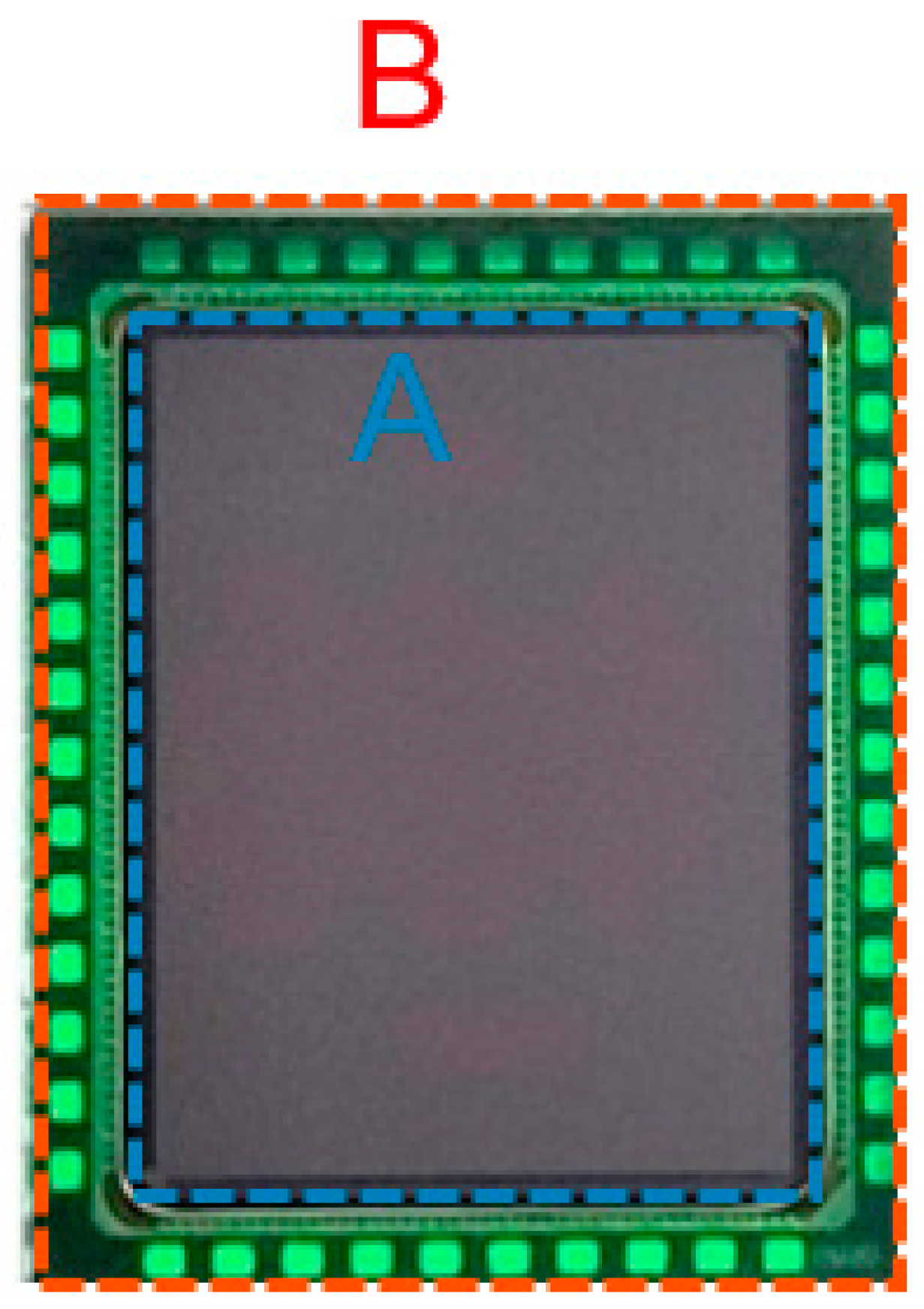
2.1. Footprint Reduction
2.2. Power Consumption Reduction
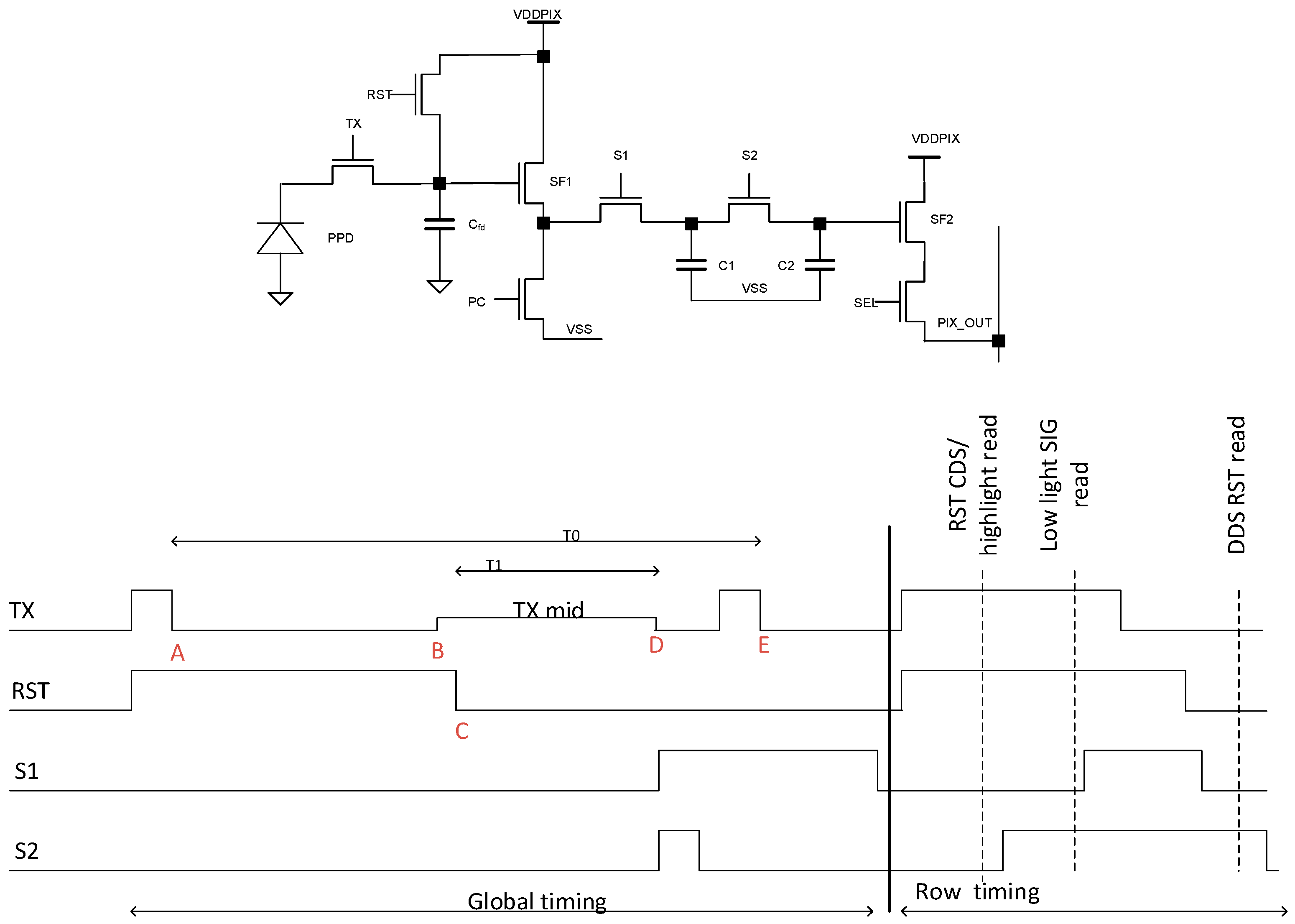
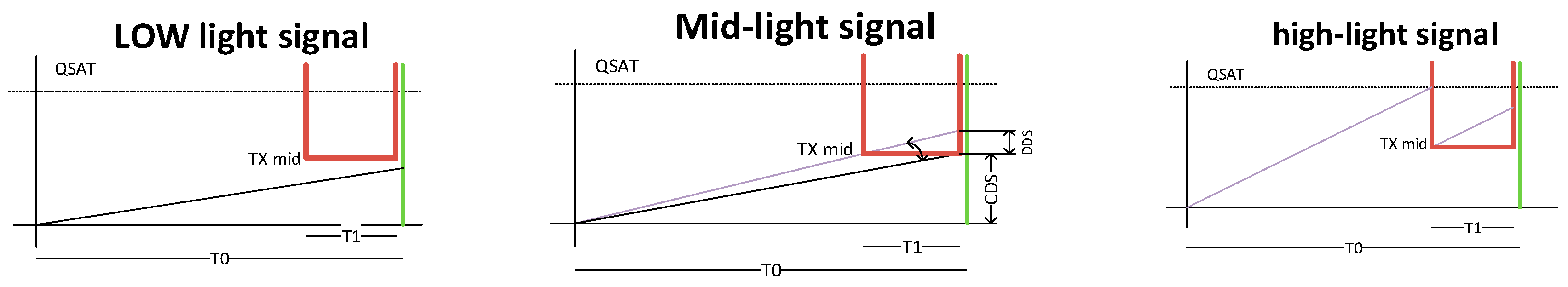
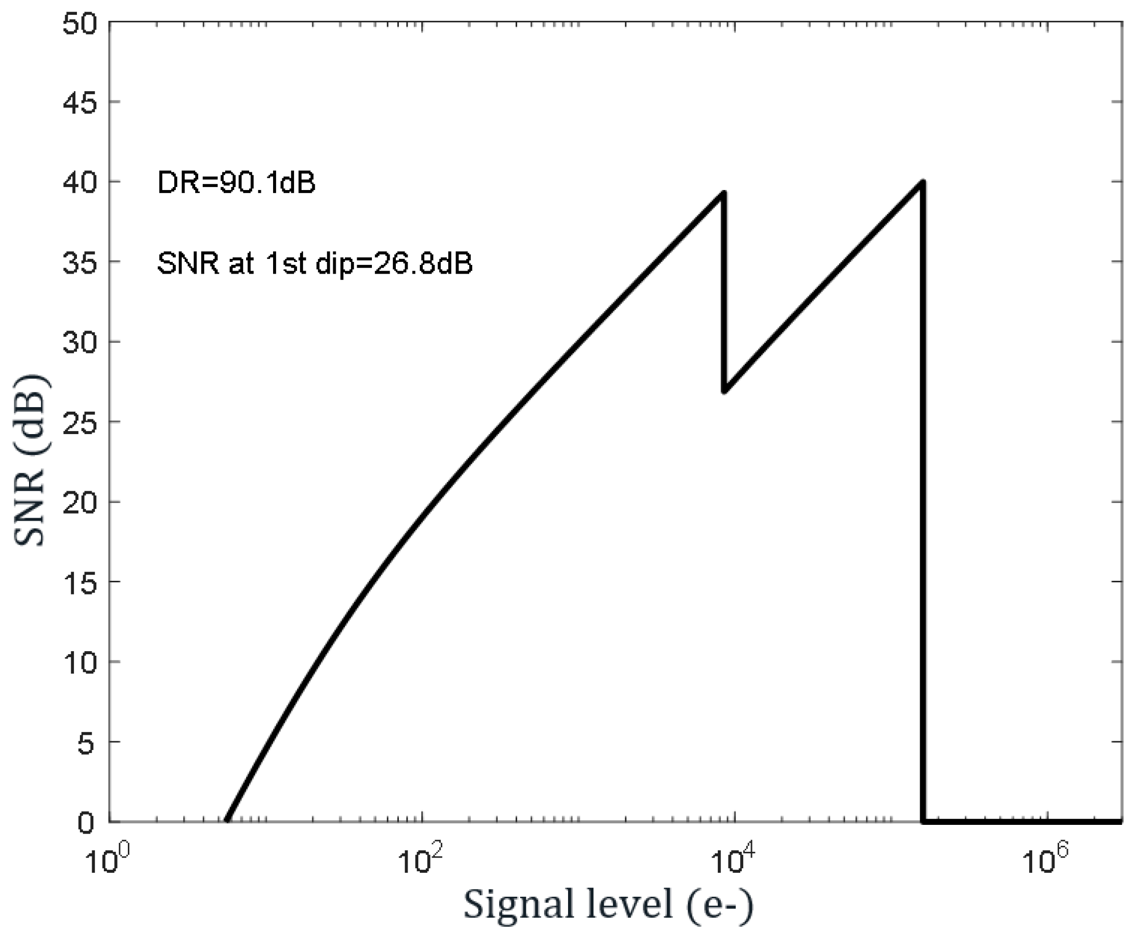
3. HDR Operation
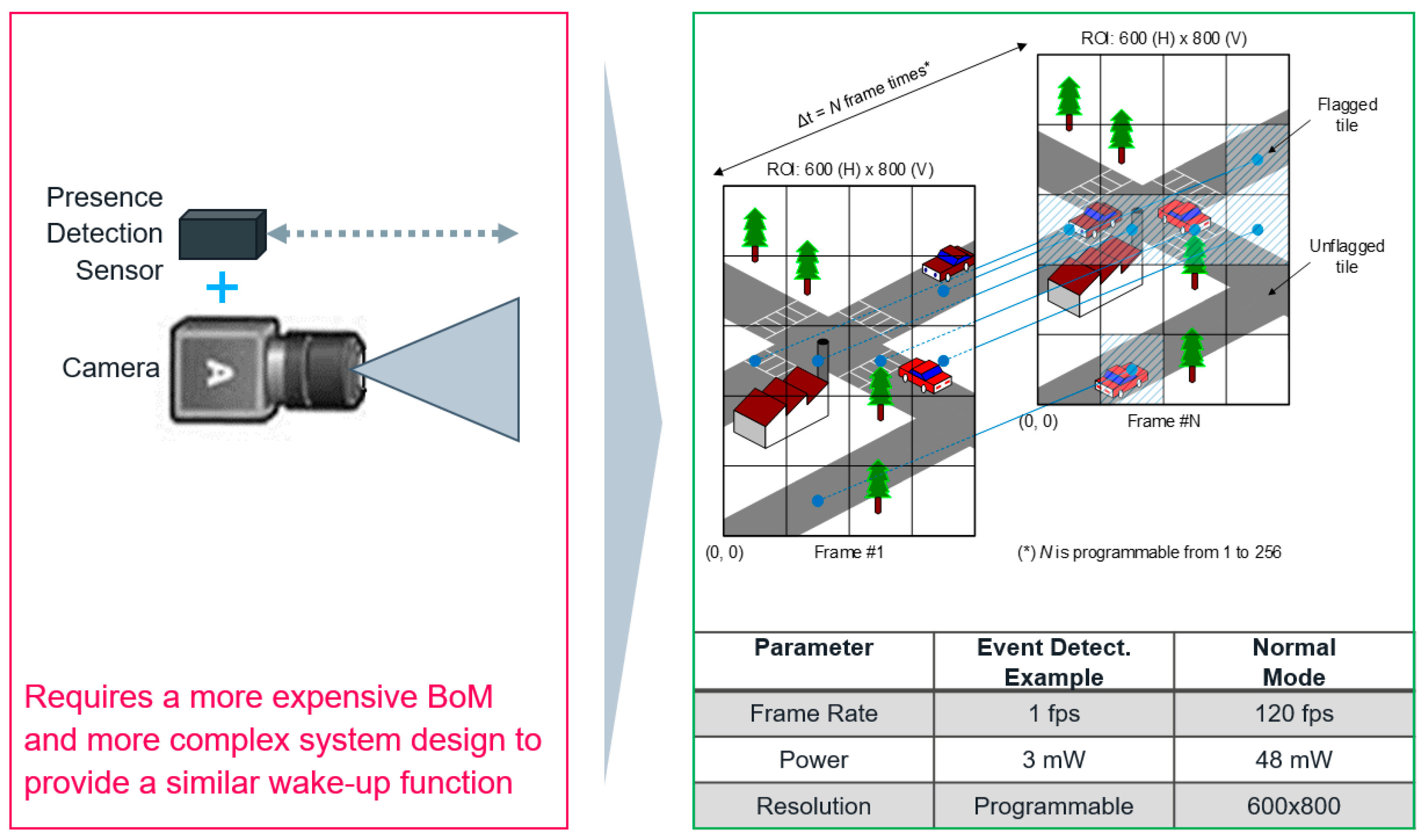
4. Event Detection Mode
5. Conclusions
Funding
Institutional Review Board Statement
Informed Consent Statement
Data Availability Statement
Conflicts of Interest
References
- Velichko, S. Overview of CMOS Global Shutter Pixels. IEEE Trans. Electron Devices 2021, 69, 2806–2814. [Google Scholar] [CrossRef]
- Meynants, G.; Walschap, T. 3d Camera System with Rolling-Shutter Image Sensor. U.S. Patent 16/755,784, 15 October 2018. [Google Scholar]
- Xhakoni, A.; Fekri, A.; Francis, P.; Vancauwenbergh, K.; Van Esbroeck, K. A 40,000 fps global shutter image sensor with 26.7 ns 12-bit row readout time. In Proceedings of the International Image Sensors Workshop (IISW), Online Event, 20–23 September 2021. [Google Scholar]
- Mizuno, I.; Tsutsui, M.; Yokoyama, T.; Hirata, T.; Nishi, Y.; Veinger, D.; Birman, A.; Lahav, A. A High-Performance 2.5 μm Charge Domain Global Shutter Pixel and Near Infrared Enhancement with Light Pipe Technology. Sensors 2020, 20, 307. [Google Scholar] [CrossRef] [PubMed]
- Oike, Y. Evolution of Image Sensor Architectures With Stacked Device Technologies. IEEE Trans. Electron Devices 2022, 69, 2757–2765. [Google Scholar] [CrossRef]
- Xhakoni, A.; Fekri, A.; Francis, P.; Melsen, S.; Janardhan, S.; Hashani, B.; Popa, A.; Ruythooren, K.; De Wit, P.; Lafaille, R.; et al. A 90 dB Single-Shot HDR, 0.5 MP Global-Shutter Image Sensor with NIR QE Enhancement, 20 mW Power Consumption and Smart Event Detection Modes. In Proceedings of the 2023 International Image Sensors Workshop, Crieff, Scotland, 21–25 May 2023. [Google Scholar]
- Kim, S.S.; Lee, G.D.R.; Park, S.S.; Shim, H.; Kim, D.H.; Choi, M.; Kim, S.; Park, G.; Oh, S.J.; Moon, J.; et al. 3-Layer Stacked Voltage-Domain Global Shutter CMOS Image Sensor with 1.8 μm-Pixel-Pitch. In Proceedings of the 2022 International Electron Devices Meeting (IEDM), San Francisco, CA, USA, 3–7 December 2022; pp. 37.5.1–37.5.4. [Google Scholar] [CrossRef]
- Ono, A.; Hashimoto, K.; Yoshinaga, T.; Teranishi, N. Near-Infrared Sensitivity Enhancement of Silicon Image Sensor with Wide Incident Angle. In Proceedings of the 2023 International Image Sensors Workshop, Crieff, Scotland, 21–25 May 2023. [Google Scholar]
- Liu, C.; Chen, S.; Tsai, T.H.; De Salvo, B.; Gomez, J. Augmented Reality—The Next Frontier of Image Sensors and Compute Systems. In Proceedings of the 2022 IEEE International Solid-State Circuits Conference (ISSCC), San Francisco, CA, USA, 20–26 February 2022; pp. 426–428. [Google Scholar] [CrossRef]
- Park, G.; Hsuing, A.C.W.; Mabuchi, K.; Yao, J.; Lin, Z.; Venezia, V.C.; Yu, T.; Yang, Y.S.; Dai, T.; Grant, L.A. A 2.2 μm stacked back side illuminated voltage domain global shutter CMOS image sensor. In Proceedings of the 2019 IEEE International Electron Devices Meeting (IEDM), San Francisco, CA, USA, 7–11 December 2019; pp. 16.4.1–16.4.4. [Google Scholar] [CrossRef]
- Meynants, G.; Bogaerts, J.; Wolfs, B.; Ceulemans, B.; De Ridder, T.; Gvozdenović, A.; Gillisjans, E.; Salmon, X.; VandeVelde, G. 24 MPixel 36 × 24 mm2 14 Bit Image Sensor in 110/90 nm CMOS Technology. In Proceedings of the International Image Sensors Workshop (IISW), Snowbird, UT, USA, 12–16 June 2013. [Google Scholar]
- Meynants, G.; Beeckman, G.; Van Wichelen, K.; De Ridder, T.; Koch, M.; Schippers, G.; Bonnifait, M.; Diels, W.; Bogaerts, J. Backside Illuminated 84 dB Global Shutter Image Sensor. In Proceedings of the International Image Sensors Workshop (IISW), Vaals, The Netherlands, 8–11 June 2015. [Google Scholar]
- Meynants, G.; Wolfs, B.; Bogaerts, J.; Li, P.; Li, Z.; Li, Y.; Creten, Y.; Ruythooren, K.; Francis, P.; Lafaille, R.; et al. A 47 MPixel 36.4 × 27.6 mm2 30 fps Global Shutter Image Sensor. In Proceedings of the International Image Sensors Workshop (IISW), Hiroshima, Japan, 30 May–2 June 2017. [Google Scholar]
- Chossat, J. Image Sensors in 3D Stacking Technology: Retrospective and Perspectives from a Digital Architect’s Point of View. In Proceedings of the 2023 International Image Sensors Workshop, Crieff, Scotland, 21–25 May 2023. [Google Scholar]
- Ikeno, R.; Mori, K.; Uno, M.; Miyauchi, K.; Isozaki, T.; Takayanagi, I.; Nakamura, J.; Wuu, S.G.; Bainbridge, L.; Berkovich, A.; et al. A 4.6-μm, 127-dB Dynamic Range, Ultra-Low Power Stacked Digital Pixel Sensor With Overlapped Triple Quantization. IEEE Trans. Electron Devices 2022, 69, 2943–2950. [Google Scholar] [CrossRef]
- Cremers, B.; Freson, T.; Esquenet, C.; Vroom, W.; Prathipati, A.K.; Okcan, B.; Luypaert, C.; Jiang, H.; Witters, H.; Compiet, J.; et al. A 5MPixel Image Sensor with a 3.45 µm Dual Storage Global Shutter Back-Side Illuminated Pixel with 90 dB DR. In Proceedings of the 2023 International Image Sensors Workshop, Crieff, Scotland, 21–25 May 2023. [Google Scholar]
- Miyauchi, K.; Mori, K.; Otaka, T.; Isozaki, T.; Yasuda, N.; Tsai, A.; Sawai, Y.; Owada, H.; Takayanagi, I.; Nakamura, J. A Stacked Back Side-Illuminated Voltage Domain Global Shutter CMOS Image Sensor with a 4.0 μm Multiple Gain Readout Pixel. Sensors 2020, 20, 486. [Google Scholar] [CrossRef] [PubMed]
- Sugawa, S.; Akahane, N.; Adachi, S.; Mori, K.; Ishiuchi, T.; Mizobuchi, K. A 100 dB dynamic range CMOS image sensor using a lateral overflow integration capacitor. In Proceedings of the 2005 IEEE International Digest of Technical Papers, Solid-State Circuits Conference, San Francisco, CA, USA, 6–10 February 2005; Volume 1, pp. 352–603. [Google Scholar] [CrossRef]
- Takayanagi, I.; Miyauchi, K.; Okura, S.; Mori, K.; Nakamura, J.; Sugawa, S. A 120-ke− Full-Well Capacity 160-µV/e− Conversion Gain 2.8-µm Backside-Illuminated Pixel with a Lateral Overflow Integration Capacitor. Sensors 2019, 19, 5572. [Google Scholar] [CrossRef] [PubMed]
- Yadid-Pecht, O.; Fossum, E.R. Wide intrascene dynamic range CMOS APS using dual sampling. IEEE Trans. Electron Devices 1997, 44, 1721–1723. [Google Scholar] [CrossRef]
- Solhusvik, J.; Kuang, J.; Lin, Z.; Manabe, S.; Lyu, J.H.; Rhodes, H. A Comparison of High Dynamic Range CIS Technologies for Automotive Applications. In Proceedings of the International Image Sensors Workshop (IISW), Snowbird, UT, USA, 12–16 June 2013. [Google Scholar]
- Xu, C.; Mo, Y.; Ren, G.; Ma, W.; Wang, X.; Shi, W.; Hou, J.; Shao, K.; Wang, H.; Xiao, P.; et al. 5.1 A Stacked Global-Shutter CMOS Imager with SC-Type Hybrid-GS Pixel and Self-Knee Point Calibration Single Frame HDR and On-Chip Binarization Algorithm for Smart Vision Applications. In Proceedings of the 2019 IEEE International Solid-State Circuits Conference—(ISSCC), San Francisco, CA, USA, 17–21 February 2019; pp. 94–96. [Google Scholar] [CrossRef]


| Mode | Power Consumption |
|---|---|
| 30 fps, 10 bits | 18.5 mW |
| 60 fps, 10 bits | 30 mW |
| 120 fps, 10 bits | 48 mW |
| 200 fps, 10 bits | 75 mW |
| Parameter | [7] | [10] | [17] | [16] | This Work |
|---|---|---|---|---|---|
| technology | Triple-Stacked 65 nm + 65 nm + 45 nm | stacked 45 nm − 65 nm | stacked 45 nm − 65 nm | stacked 45 nm − 65 nm | stacked 45 nm + 40 nm |
| Pixel pitch (µm) | 1.8 | 2.2 | 4 | 3.45 | 2.79 |
| Resolution | 1280 × 1024 | 640 × 480 | 1024 × 832 | 5 MP | 600 × 800 |
| Shutter | Global VD | Global VD | Global VD | Global VD | Global VD |
| DR (dB) | 68 (HCG) | 61 | 90 | 90 | 90 |
| Noise (e−) | 1.8 (HCG) | 2.3 (HCG mode) | 4 | 2.7 (HCG) | 5 (LCG mode) |
| Power (mW) | - | 139 | - | - | <20 mW @10 b, 30 fps, 48 mW @120 fps |
| Footprint efficiency ratio (%) * | - | 19.2 | 21.3 | - | 58 |
| Footprint (mm × mm) | - | 2.6 × 2.95 | 8 × 8 | - | 2.3 × 2.8 |
| QE 940 nm (%) | Only visible reported | 38 | 40 | 41 | 36 |
Disclaimer/Publisher’s Note: The statements, opinions and data contained in all publications are solely those of the individual author(s) and contributor(s) and not of MDPI and/or the editor(s). MDPI and/or the editor(s) disclaim responsibility for any injury to people or property resulting from any ideas, methods, instructions or products referred to in the content. |
© 2023 by the author. Licensee MDPI, Basel, Switzerland. This article is an open access article distributed under the terms and conditions of the Creative Commons Attribution (CC BY) license (https://creativecommons.org/licenses/by/4.0/).
Share and Cite
Xhakoni, A. A 0.5 MP, 3D-Stacked, Voltage-Domain Global Shutter Image Sensor with NIR QE Enhancement, Event Detection Modes, and 90 dB Dynamic Range. Sensors 2023, 23, 9448. https://doi.org/10.3390/s23239448
Xhakoni A. A 0.5 MP, 3D-Stacked, Voltage-Domain Global Shutter Image Sensor with NIR QE Enhancement, Event Detection Modes, and 90 dB Dynamic Range. Sensors. 2023; 23(23):9448. https://doi.org/10.3390/s23239448
Chicago/Turabian StyleXhakoni, Adi. 2023. "A 0.5 MP, 3D-Stacked, Voltage-Domain Global Shutter Image Sensor with NIR QE Enhancement, Event Detection Modes, and 90 dB Dynamic Range" Sensors 23, no. 23: 9448. https://doi.org/10.3390/s23239448
APA StyleXhakoni, A. (2023). A 0.5 MP, 3D-Stacked, Voltage-Domain Global Shutter Image Sensor with NIR QE Enhancement, Event Detection Modes, and 90 dB Dynamic Range. Sensors, 23(23), 9448. https://doi.org/10.3390/s23239448