
High Gain Flat-Panel mmWave Antenna Array


Abstract
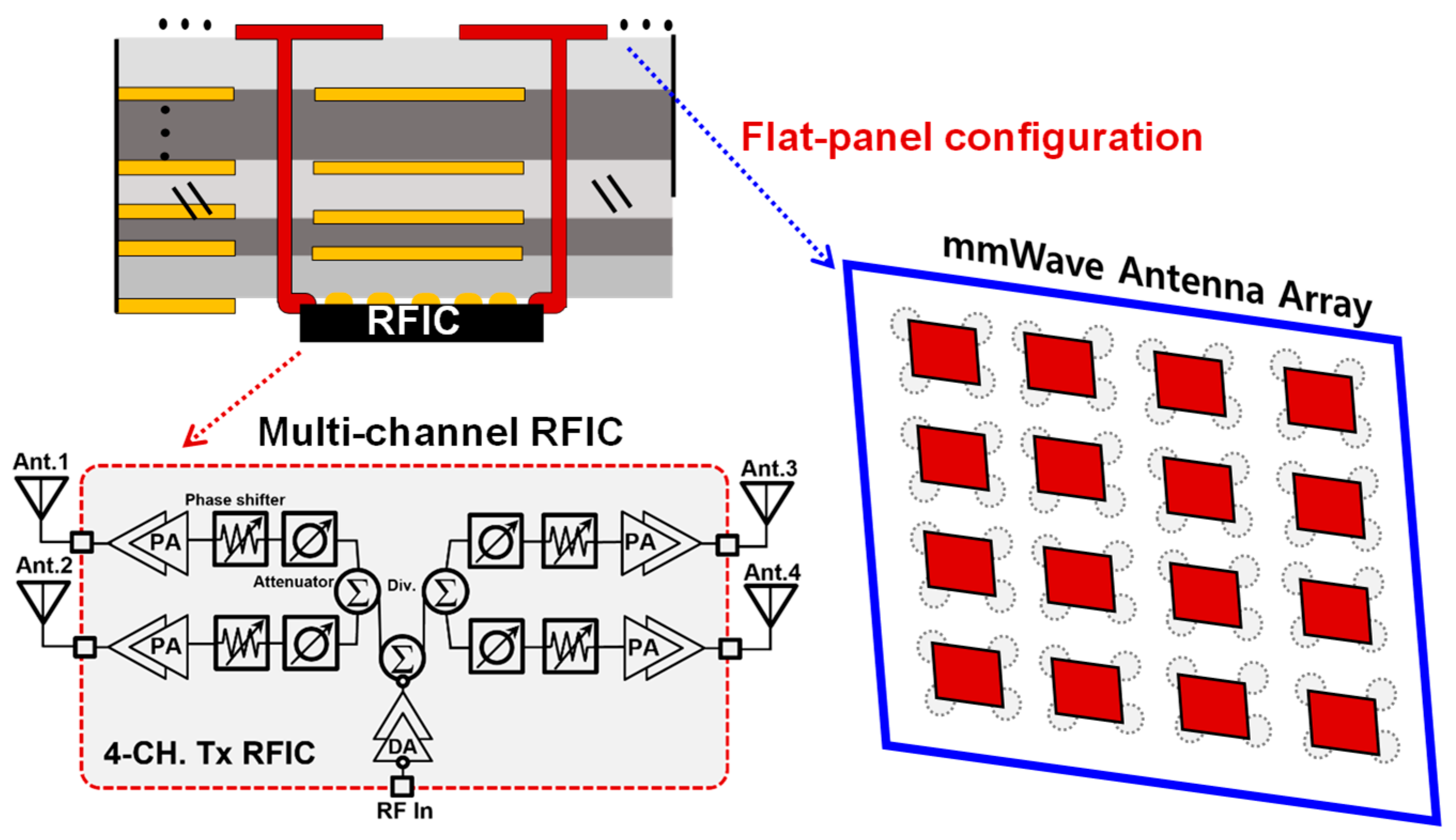
:1. Introduction
- An extended analysis of a high-gain antenna element [17] for an array antenna application.
- The design and verification of a feed network tailored for the high-gain antenna array, implemented with a 4 × 4 array antenna.
- The development and validation of an optimized 4 × 4 high gain antenna array tailored for the n257 band.
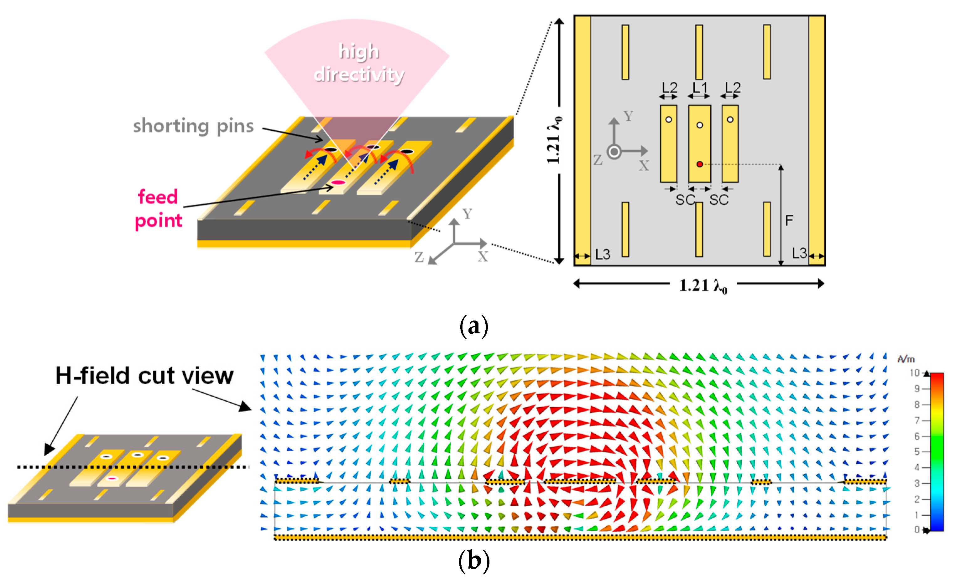
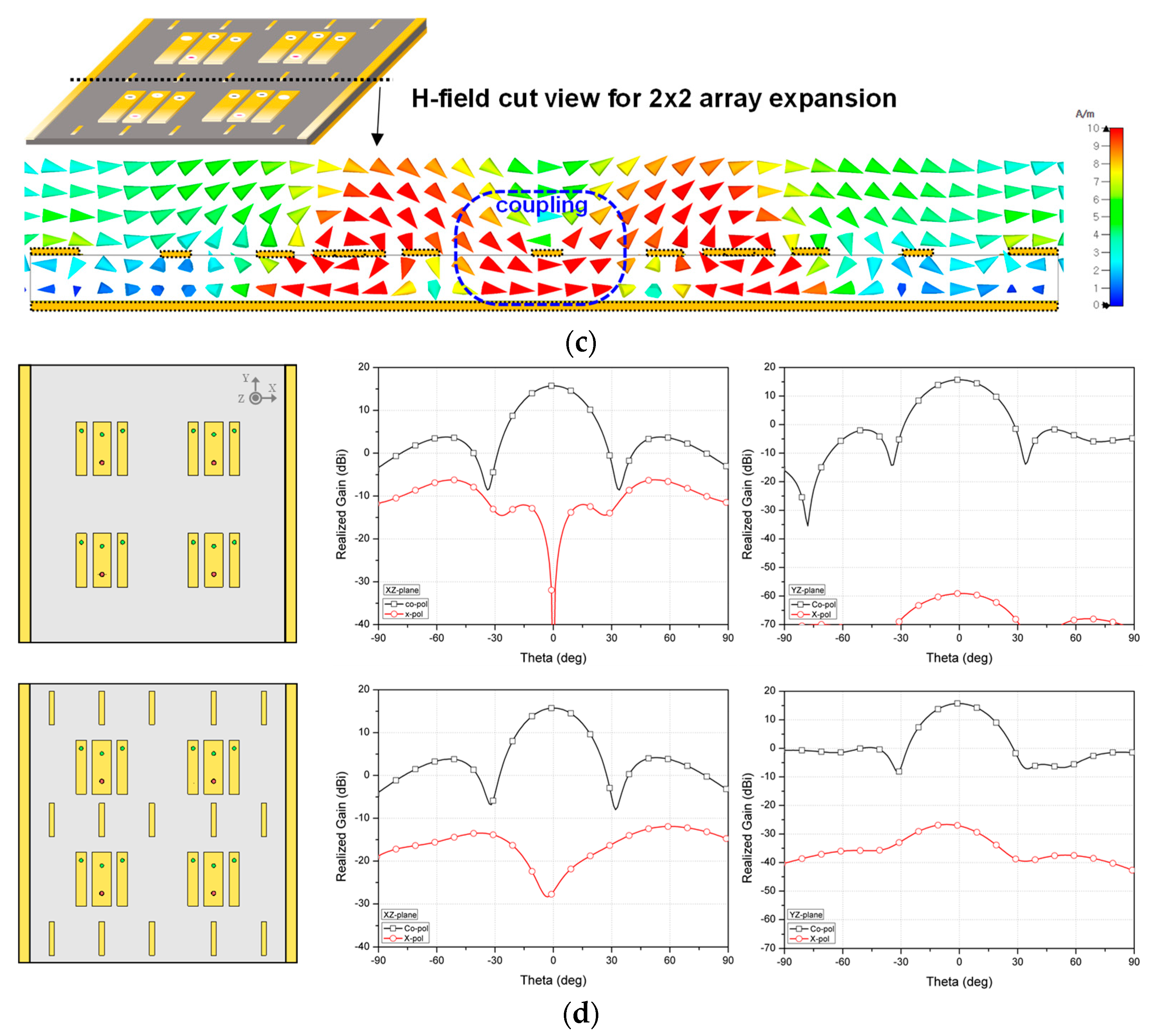
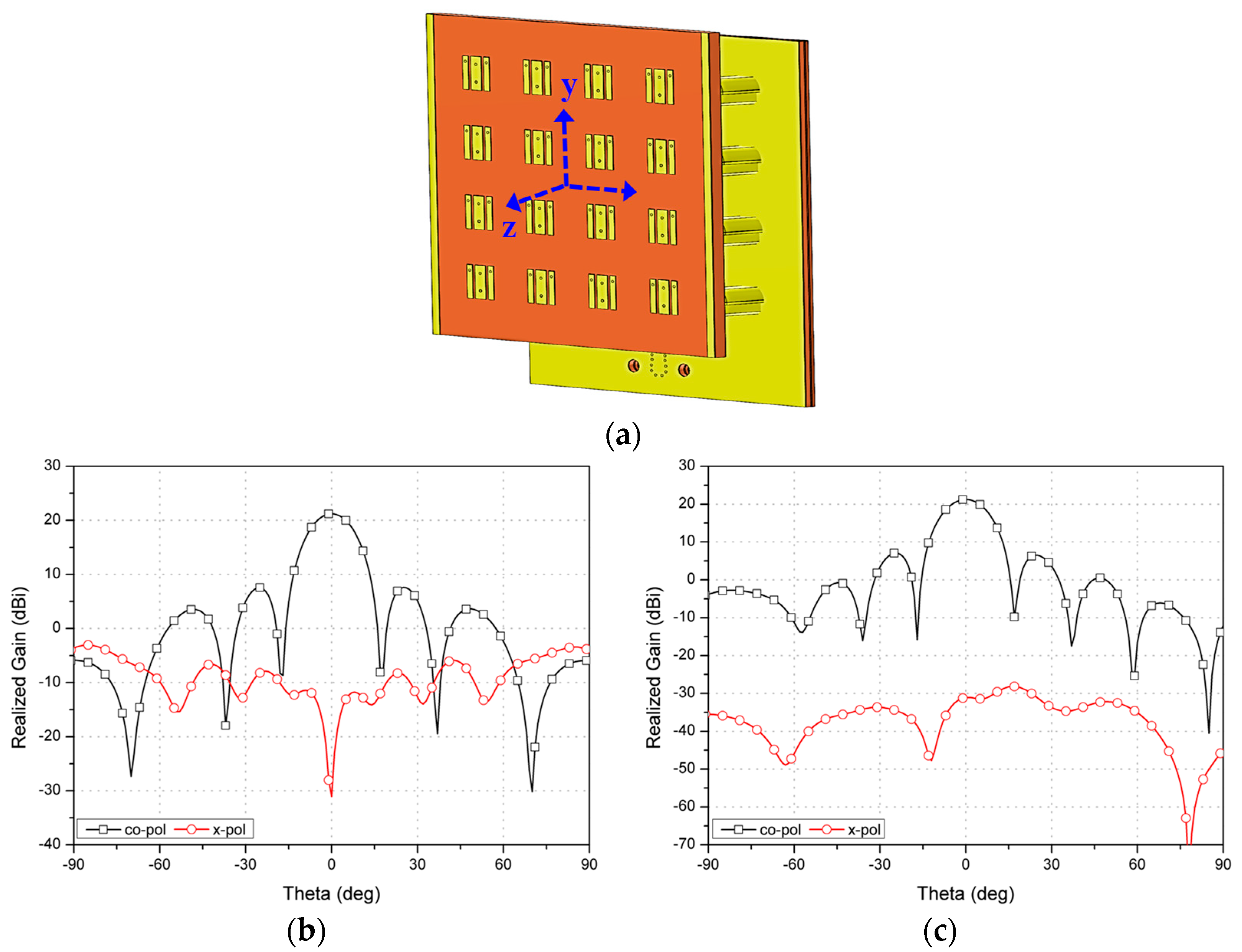
2. Design and Analysis
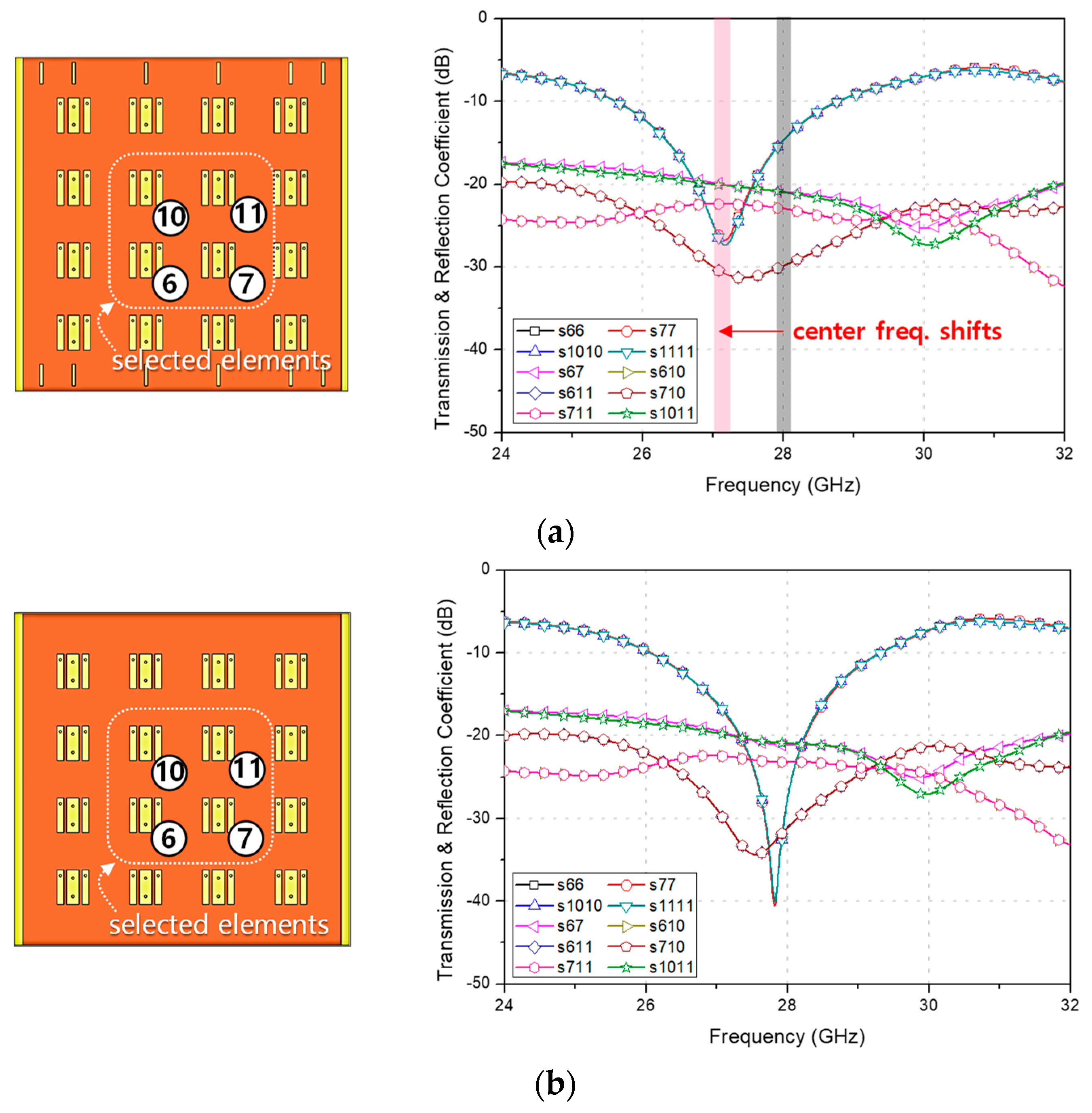
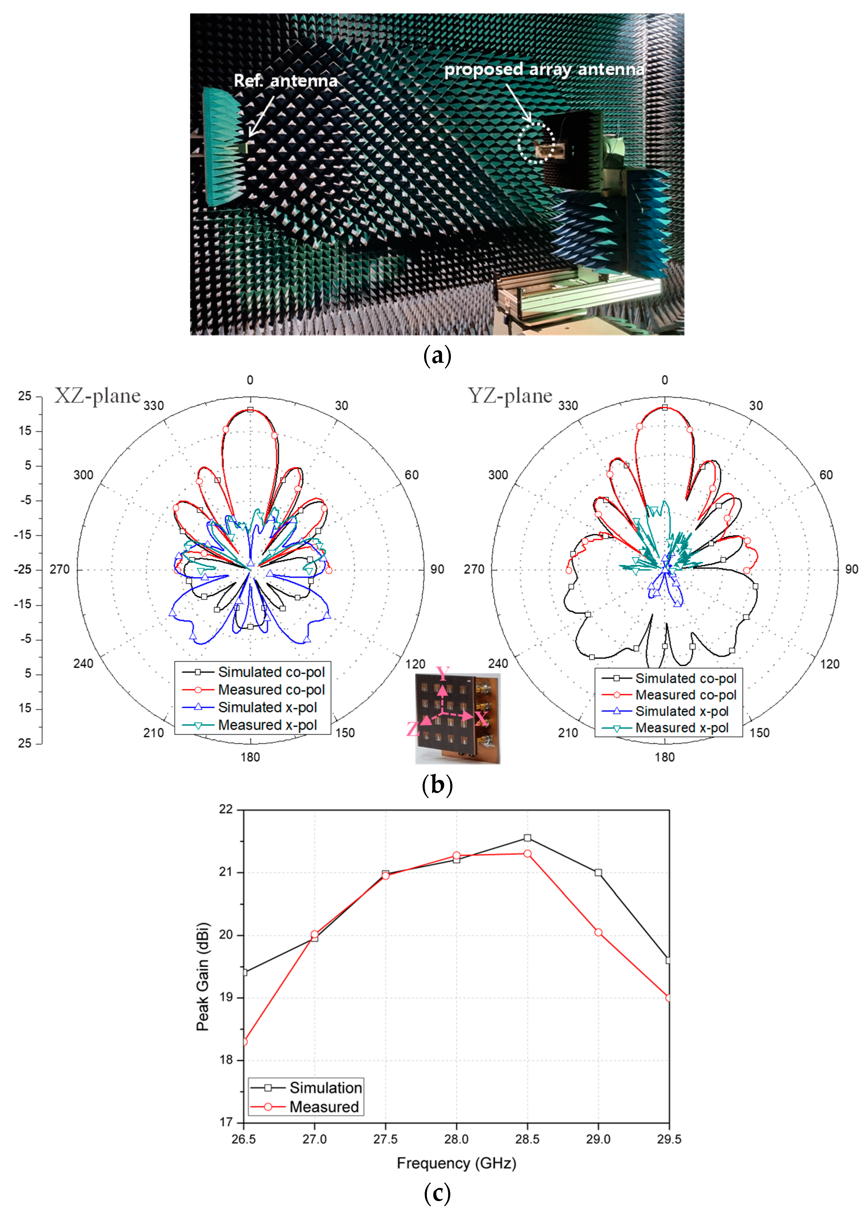
3. Fabrication and Measurement
4. Discussion
5. Conclusions
Author Contributions
Funding
Institutional Review Board Statement
Informed Consent Statement
Data Availability Statement
Conflicts of Interest
References
- Chieh, J.-C.S.; Yeo, E.; Farkouh, R.; Castro, A.; Kerber, M.; Olsen, R.B.; Merulla, E.J.; Sharma, S.K. Development of Flat Panel Active Phased Array Antennas Using 5G Silicon RFICs at Ku- and Ka-Bands. IEEE Access 2020, 8, 192669–192681. [Google Scholar] [CrossRef]
- Ozpinar, H.; Aksimsek, S.; Tokan, N.T. A Novel Compact, Broadband, High Gain Millimeter-Wave Antenna for 5G Beam Steering Applications. IEEE Trans. Veh. Technol. 2020, 69, 2389–2397. [Google Scholar] [CrossRef]
- Mao, C.-X.; Gao, S.; Wang, Y. Broadband High-Gain Beam-Scanning Antenna Array for Millimeter-Wave Applications. IEEE Trans. Antennas Propag. 2017, 65, 4864–4868. [Google Scholar] [CrossRef]
- Wang, H.; Kedze, K.E.; Park, I. A High-Gain and Wideband Series-Fed Angled Printed Dipole Array Antenna. IEEE Trans. Antennas Propag. 2020, 68, 5708–5713. [Google Scholar] [CrossRef]
- Zhai, G.; Cheng, Y.; Yin, Q.; Zhu, S.; Gao, J. Gain Enhancement of Printed Log-Periodic Dipole Array Antenna Using Director Cell. IEEE Trans. Antennas Propag. 2014, 62, 5915–5919. [Google Scholar] [CrossRef]
- Chu, Q.; Li, X.; Ye, M. High-Gain Printed Log-Periodic Dipole Array Antenna with Parasitic Cell for 5G Communication. IEEE Trans. Antennas Propag. 2017, 65, 6338–6344. [Google Scholar] [CrossRef]
- Baldazzi, E.; Al-Rawi, A.; Cicchetti, R.; Smolders, A.B.; Testa, O.; Moreno, C.d.J.v.C.; Caratelli, D. A High-Gain Dielectric Resonator Antenna with Plastic-Based Conical Horn for Millimeter-Wave Applications. IEEE Antennas Wirel. Propag. Lett. 2020, 19, 949–953. [Google Scholar] [CrossRef]
- Chen, Z.; Shen, C.; Liu, H.; Ye, X.; Qi, L.; Yao, Y.; Yu, J.; Chen, X. Millimeter-Wave Rectangular Dielectric Resonator Antenna Array with Enlarged DRA Dimensions, Wideband Capability, and High-Gain Performance. IEEE Trans. Antennas Propag. 2020, 68, 3271–3276. [Google Scholar] [CrossRef]
- Li, X.; Xiao, J.; Qi, Z.; Zhu, H. Broadband and High-Gain SIW-Fed Antenna Array for 5G Applications. IEEE Access 2018, 6, 56282–56289. [Google Scholar] [CrossRef]
- Xiao, J.; Qi, Z.; Li, X.; Zhu, H. Broadband and High-Gain SIW-Fed Slot Array for Millimeter-Wave Applications. IEEE Trans. Antennas Propag. 2019, 67, 3484–3489. [Google Scholar] [CrossRef]
- Zhu, J.; Chu, C.; Deng, L.; Zhang, C.; Yang, Y.; Li, S. mm-Wave High Gain Cavity-Backed Aperture-Coupled Patch Antenna Array. IEEE Access 2018, 6, 44050–44058. [Google Scholar] [CrossRef]
- Peng, W.; Cao, W.; Qian, Z. High-Gain Electrically Large Air-Cavity-Backed Patch Antenna Element and Array. IEEE Access 2018, 6, 74072–74080. [Google Scholar] [CrossRef]
- Kim, Y.-J.; Kim, Y.-B.; Lee, H.L. mmWave High Gain Planar H-Shaped Shorted Ring Antenna Array. Sensors 2020, 20, 5168. [Google Scholar] [CrossRef] [PubMed]
- Hu, B.; Wu, Y.C.; Zhang, W.; Zhang, B. A Novel Metamaterial-Based Planar Integrated Luneburg Lens Antenna with Wide Bandwidth and High Gain. IEEE Access 2020, 8, 4708–4713. [Google Scholar] [CrossRef]
- Asaadi, M.; Sebak, A. Gain and Bandwidth Enhancement of 2 × 2 Square Dense Dielectric Patch Antenna Array Using a Holey Superstrate. IEEE Antennas Wirel. Propag. Lett. 2017, 16, 1808–1811. [Google Scholar] [CrossRef]
- Asaadi, M.; Afifi, I.; Sebak, A. High Gain and Wideband High Dense Dielectric Patch Antenna Using FSS Superstrate for Millimeter-Wave Applications. IEEE Access 2018, 6, 38243–38250. [Google Scholar] [CrossRef]
- Kim, J.; Lee, H.L. High Gain Planar Segmented Antenna for mmWave Phased Array Applications. IEEE Trans. Antennas Propag. 2022, 70, 5918–5922. [Google Scholar] [CrossRef]
- Sorkherizi, M.S.; Dadgarpour, A.; Kishk, A.A. Planar High-efficiency Antenna Array Using New Printed Ridge Gap Waveguide Technology. IEEE Trans. Antennas Propag. 2017, 65, 3772–3776. [Google Scholar] [CrossRef]
- Dzagbletey, P.A.; Jung, Y.-B. Stacked Microstrip Linear Array for Millimeter-Wave 5G Baseband Communication. IEEE Antennas Wirel. Propag. Lett. 2018, 17, 780–783. [Google Scholar] [CrossRef]
- Jin, H.; Che, W.; Chin, K.-S.; Yang, W.; Xue, Q. Millimeter-Wave TE20-Mode SIW Dual-Slot-Fed Patch Antenna Array With a Compact Differential Feeding Network. IEEE Trans. Antennas Propag. 2018, 66, 456–461. [Google Scholar] [CrossRef]
- Ashraf, N.; Sebak, A.R.; Kishk, A.A. Packaged Microstrip Line Feed Network on a Single Surface for Dual-Polarized 2N×2M ME-Dipole Antenna Array. IEEE Antennas Wirel. Propag. Lett. 2020, 19, 596–600. [Google Scholar] [CrossRef]
- Kim, W.; Bang, J.; Choi, J. A Cost-Effective Antenna-in-Package Design With a 4×4 Dual-Polarized High Isolation Patch Array for 5G mmWave Applications. IEEE Access 2021, 9, 163882–163892. [Google Scholar] [CrossRef]
- Ghosh, S.; Baghel, G.S.; Swati, M.V. A low-profile, high gain, dual-port, planar array antenna for mm-wave powered 5G IoT systems. AEU-Int. J. Electron. Commun. 2022, 155, 154354. [Google Scholar] [CrossRef]
- Chen, Z.; Zhang, W.; Wang, K. Single-Layer Interconnected Magneto-Electric Dipole Antenna Array for 5G Communication Applications. Electronics 2023, 12, 922. [Google Scholar] [CrossRef]


| Ref. |
Center Freq. (GHz) |
# of Antenna Elements | Total Antenna Volume ) |
Bandwidth (%) |
Realized Gain (dBi) | FoM 1 (BW/ **) | FoM 2 (Gain/ ***) |
|---|---|---|---|---|---|---|---|
| [18] | 30 | 16 (array) | 3.5 × 3.5 × 0.28 | 16.5 | 21.2 | 17.678 | 1.73 |
| [19] | 27.7 | 42 (array) | 6.88 × 8.27 × 0.047 | 6.3 | 21.8 | 37.129 | 0.383 |
| [20] | 28 | 16 (array) | 3.92 × 3.55 × 0.093 | 8.5 | 19.1 | 25.591 | 1.372 |
| [21] | 30 | 16 (array) | 5.7 × 5.7 × 0.152 | 16.7 | 19.3 | 32.96 | 0.594 |
| [22] | 30 | 16 (array) | 3.72 × 3.72 × 0.12 | 11.89 | 17.37 | 29.725 | 1.255 |
| [23] | 28 | 16 (array) | 7.34 × 2.1 × 0.047 | 4.28 | 18.2 | 25.532 | 1.18 |
| [24] | 28 | 25 (array) | 4.00 × 4.67 × 0.146 | 52 | 20.44 | 99.726 | 1.094 |
| This work | 28.5 | 16 (array) | 3.74 × 3.74 × 0.106 * | 20.6 | 21.3 * | 55.386 | 1.522 |
Disclaimer/Publisher’s Note: The statements, opinions and data contained in all publications are solely those of the individual author(s) and contributor(s) and not of MDPI and/or the editor(s). MDPI and/or the editor(s) disclaim responsibility for any injury to people or property resulting from any ideas, methods, instructions or products referred to in the content. |
© 2023 by the authors. Licensee MDPI, Basel, Switzerland. This article is an open access article distributed under the terms and conditions of the Creative Commons Attribution (CC BY) license (https://creativecommons.org/licenses/by/4.0/).
Share and Cite
Moon, S.-M.; Cho, J.; Lee, H.L. High Gain Flat-Panel mmWave Antenna Array. Sensors 2023, 23, 9433. https://doi.org/10.3390/s23239433
Moon S-M, Cho J, Lee HL. High Gain Flat-Panel mmWave Antenna Array. Sensors. 2023; 23(23):9433. https://doi.org/10.3390/s23239433
Chicago/Turabian StyleMoon, Seong-Mo, Junhyuk Cho, and Han Lim Lee. 2023. "High Gain Flat-Panel mmWave Antenna Array" Sensors 23, no. 23: 9433. https://doi.org/10.3390/s23239433
APA StyleMoon, S.-M., Cho, J., & Lee, H. L. (2023). High Gain Flat-Panel mmWave Antenna Array. Sensors, 23(23), 9433. https://doi.org/10.3390/s23239433