
An N-Type Pseudo-Static eDRAM Macro with Reduced Access Time for High-Speed Processing-in-Memory in Intelligent Sensor Hub Applications


Abstract
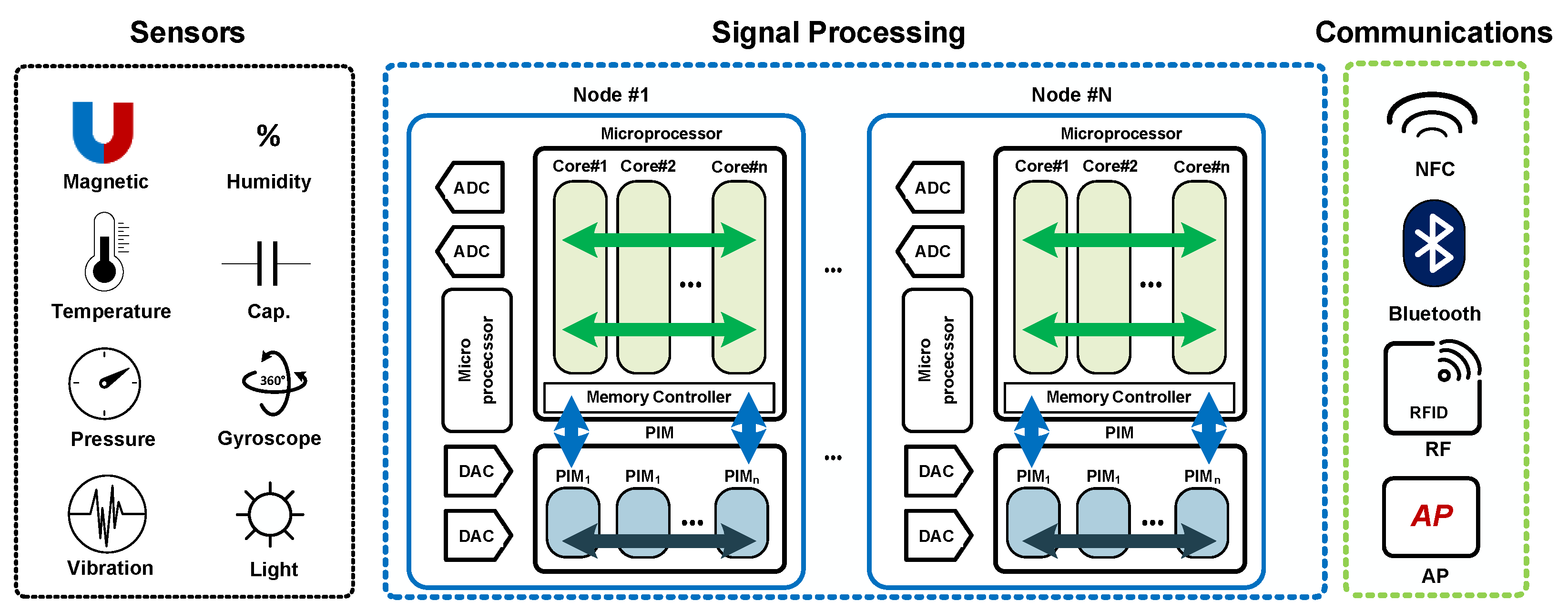
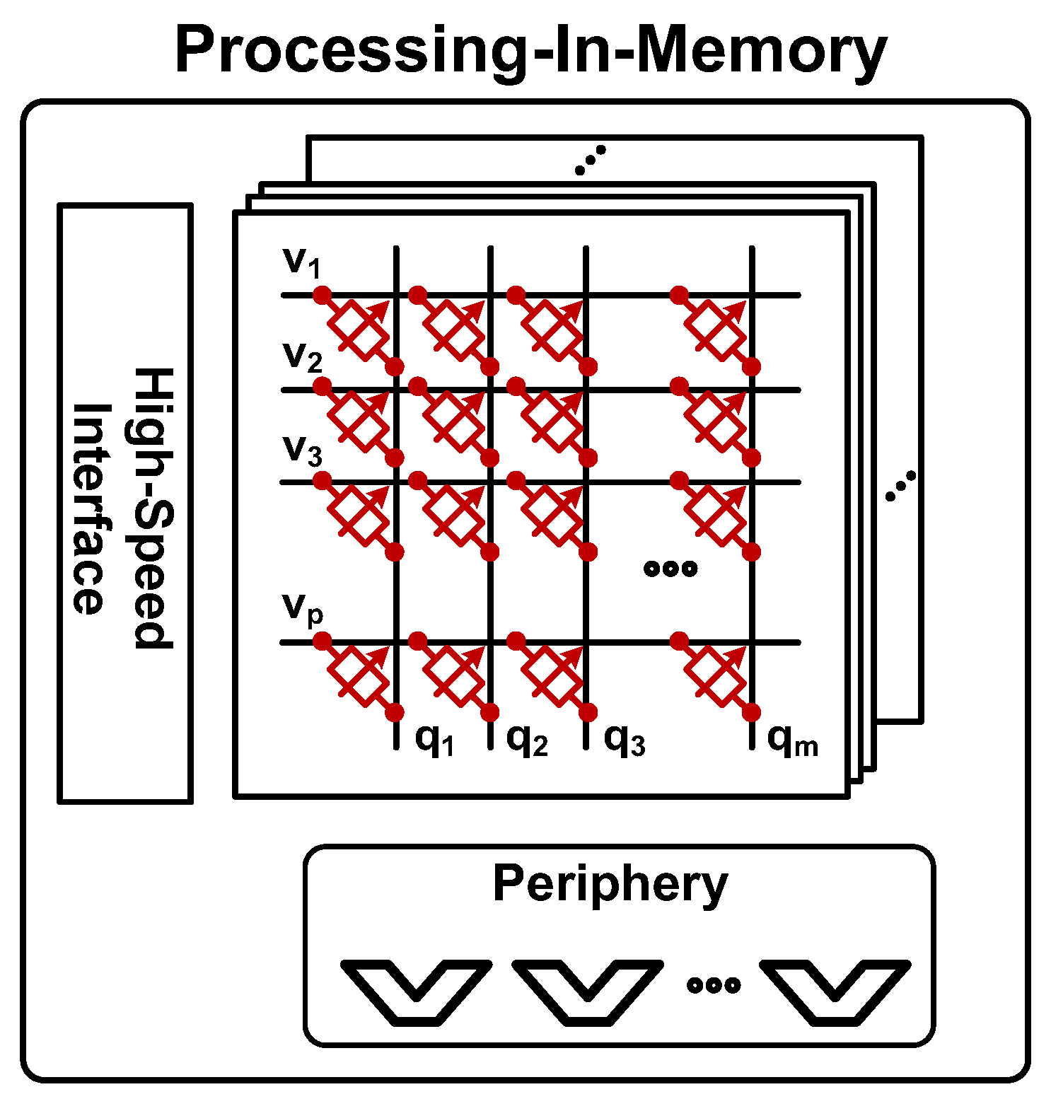
:1. Introduction
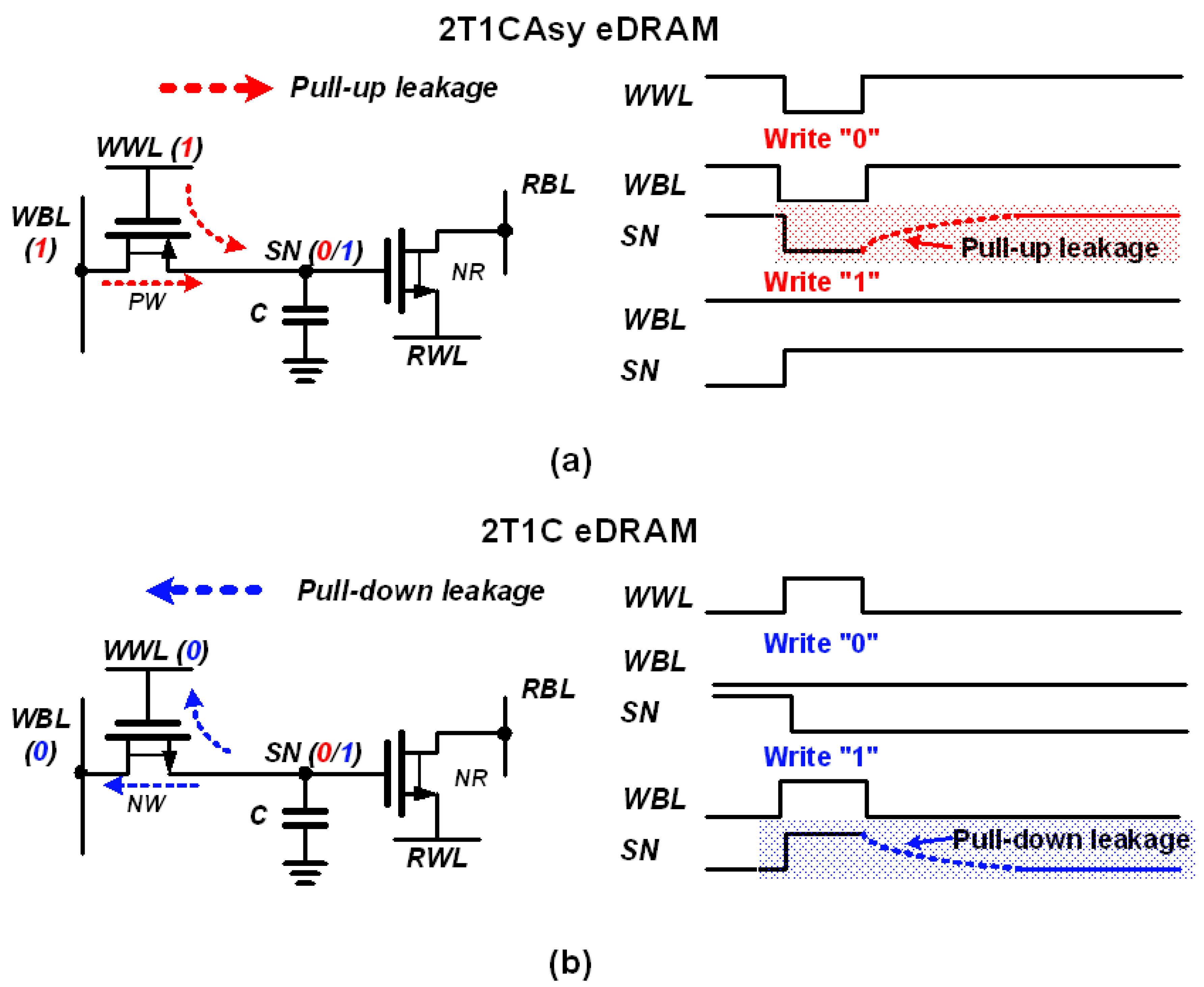
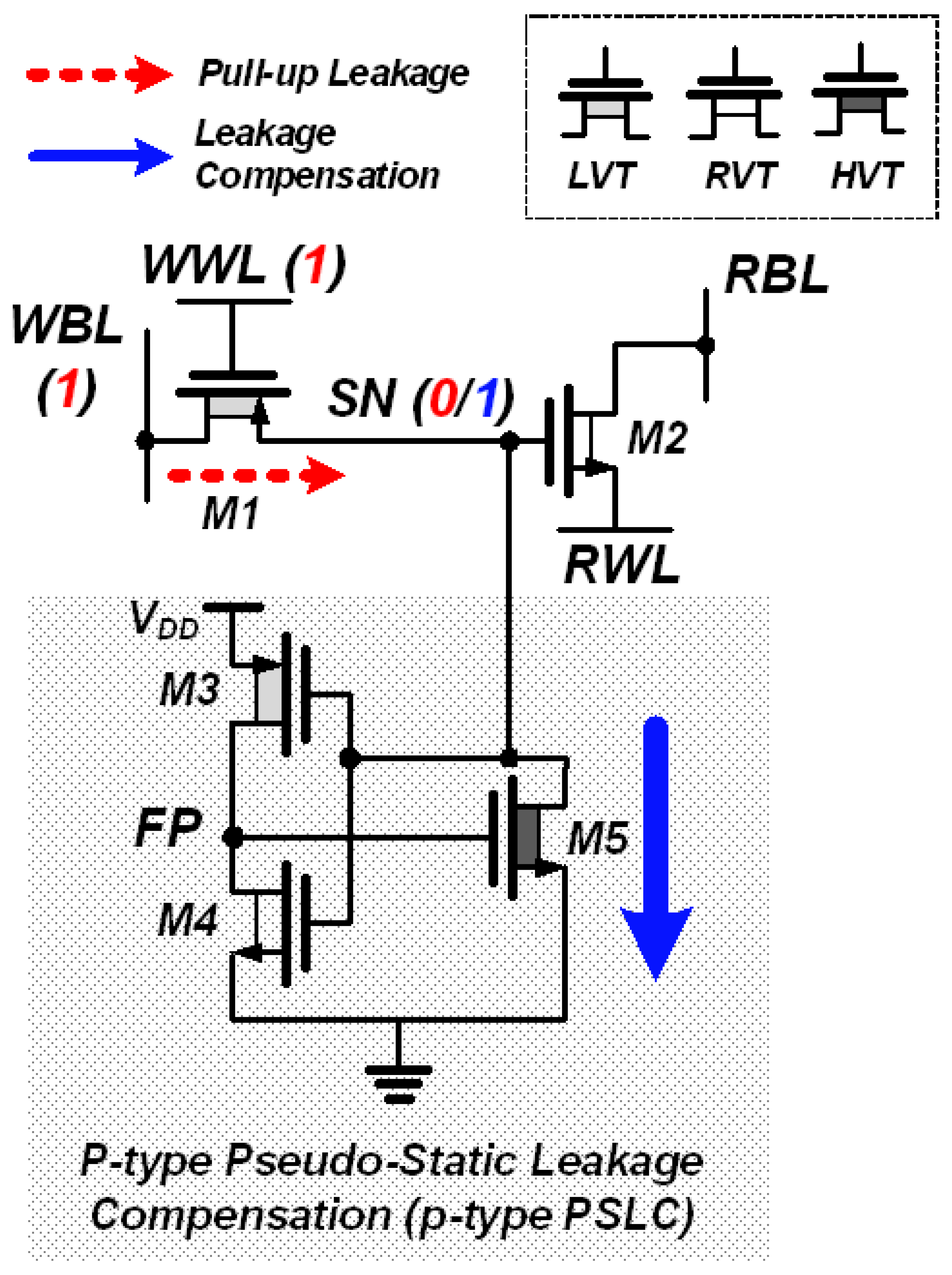
2. Overview of eDRAM Gain Cell Topologies and Limitations of Previous Work
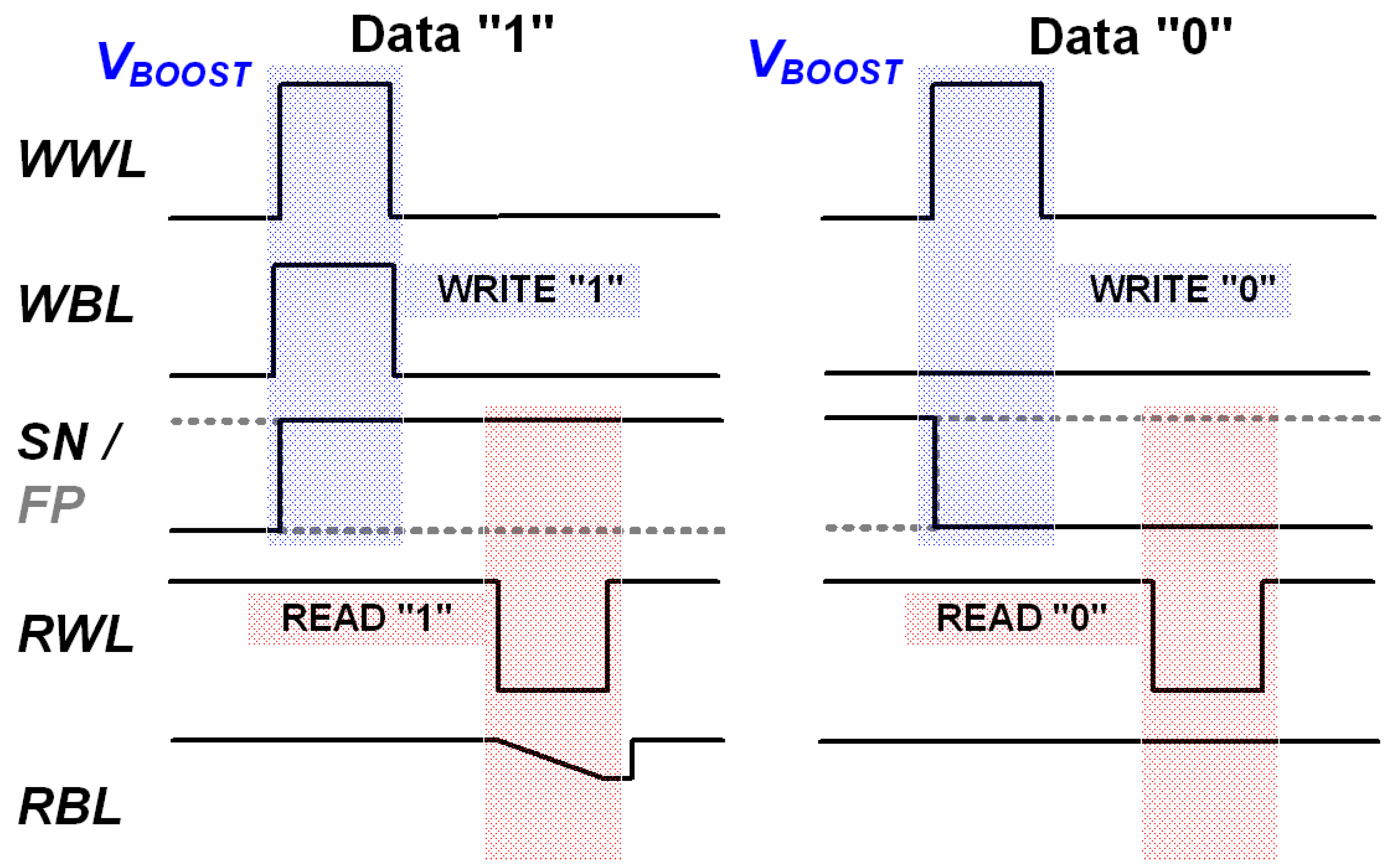
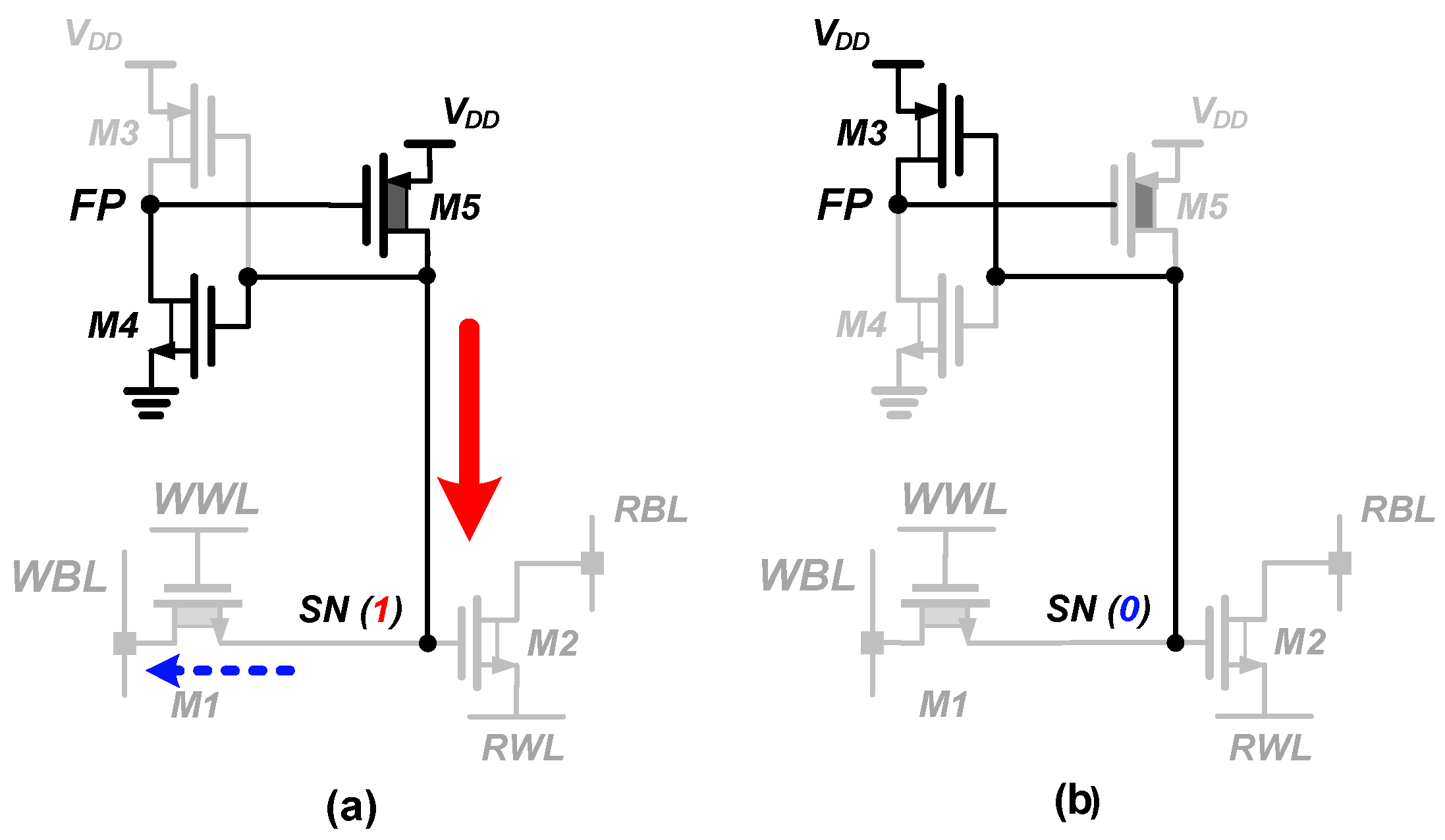
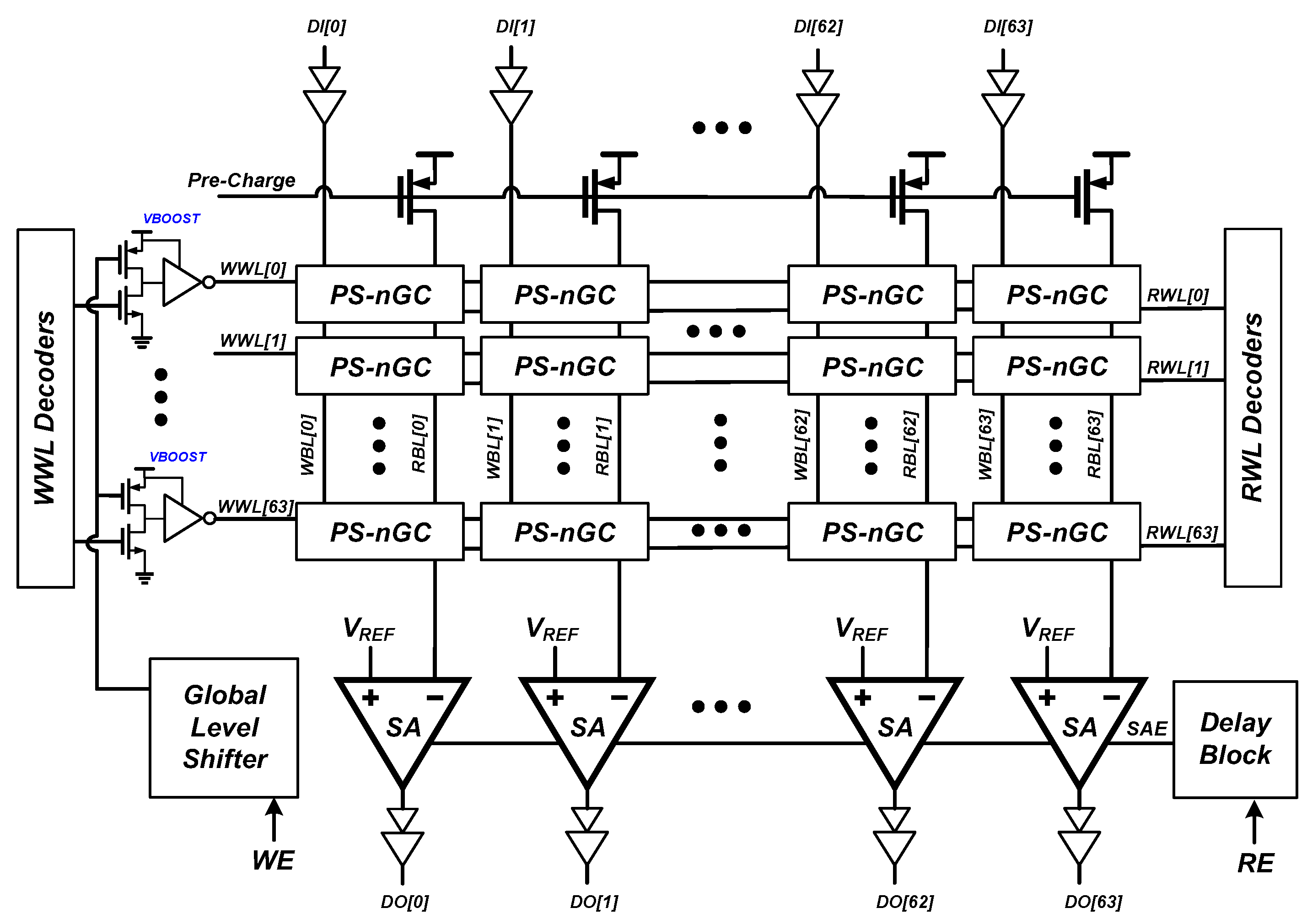
3. Operating Principle and Circuit Implementation of Proposed PS-nGC
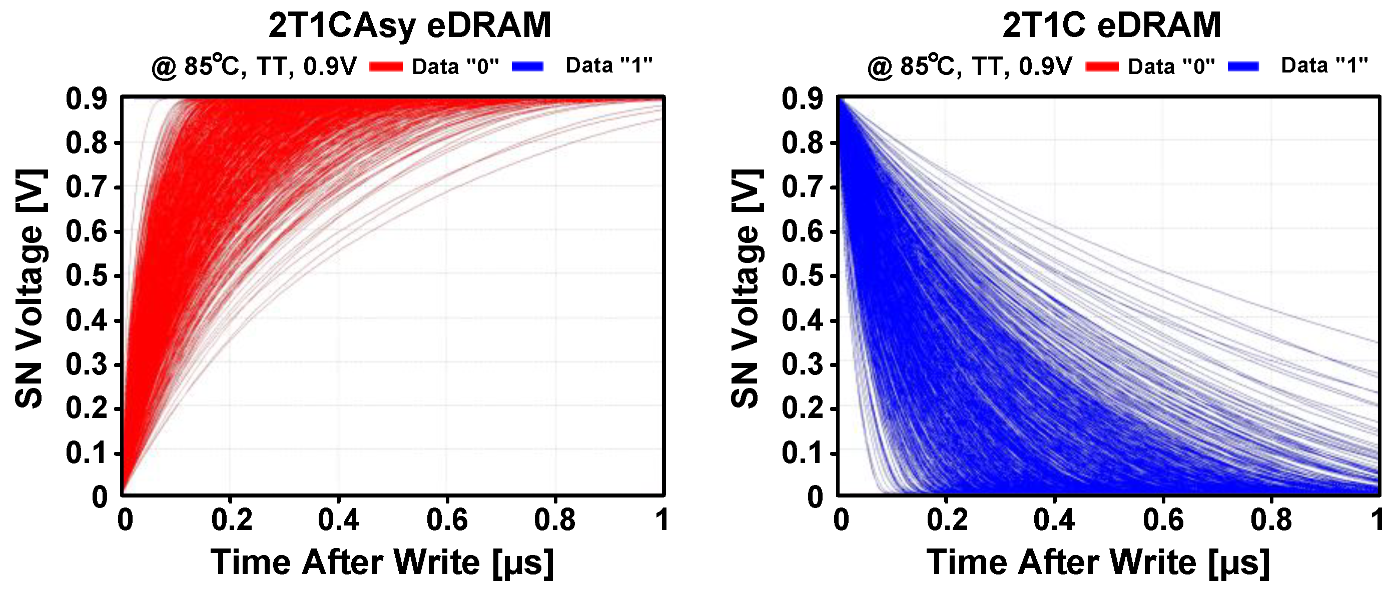
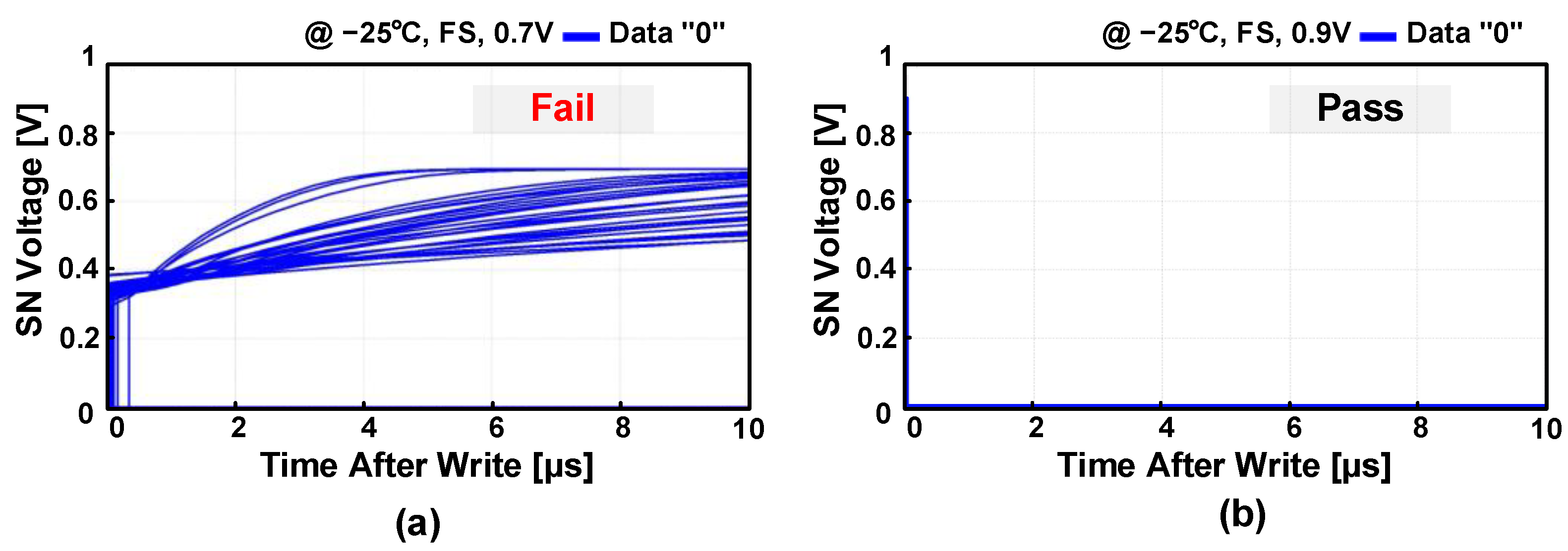
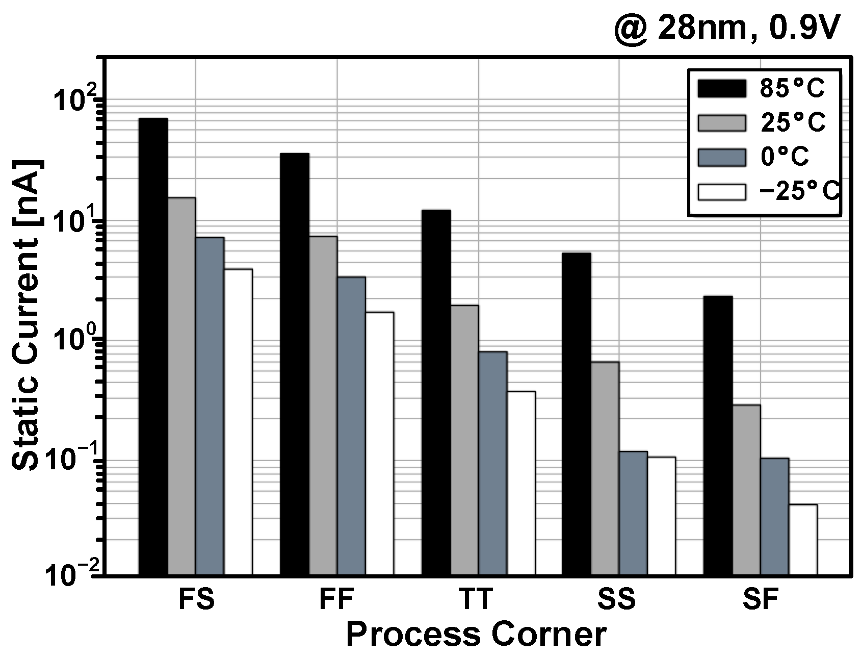
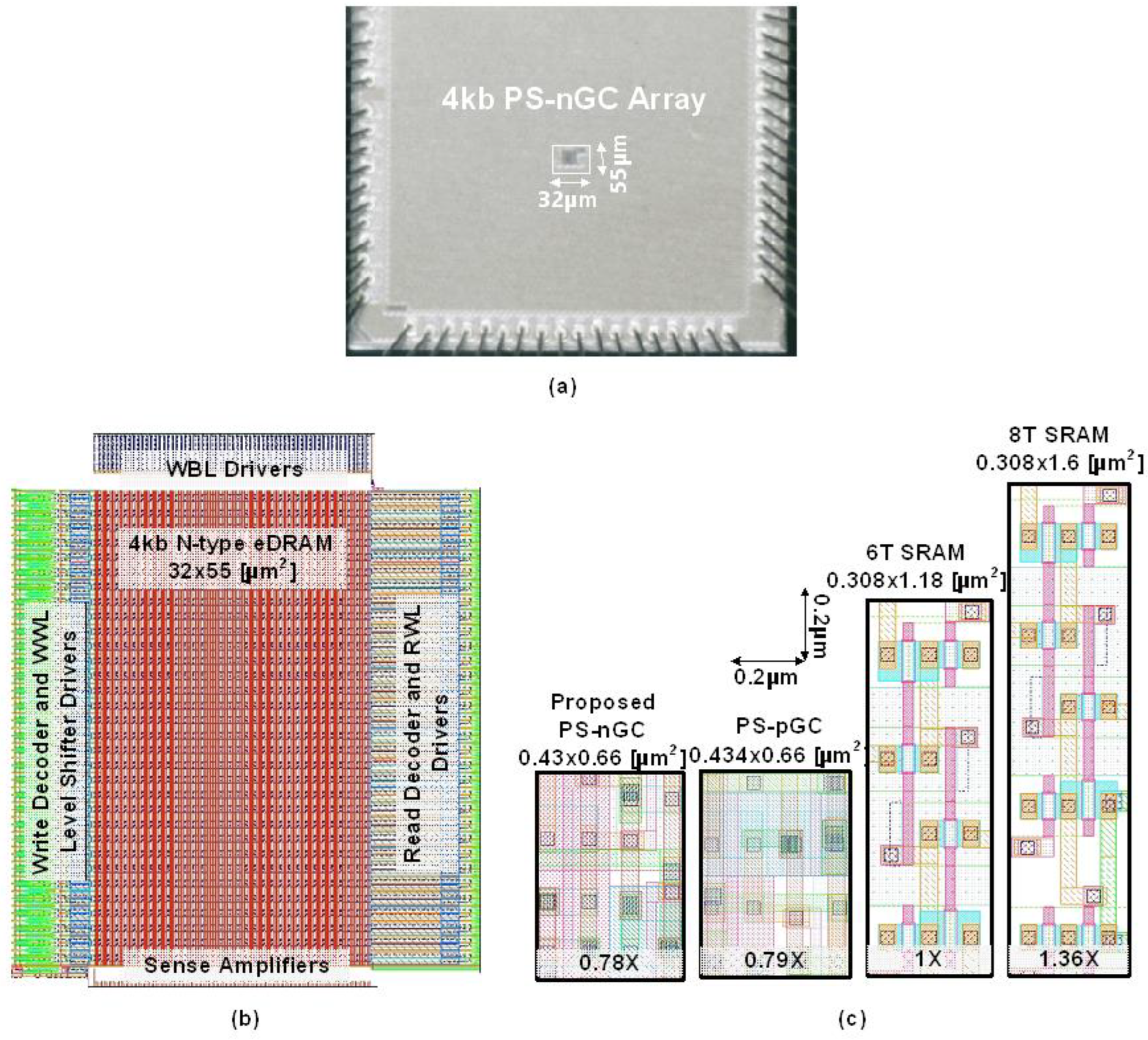
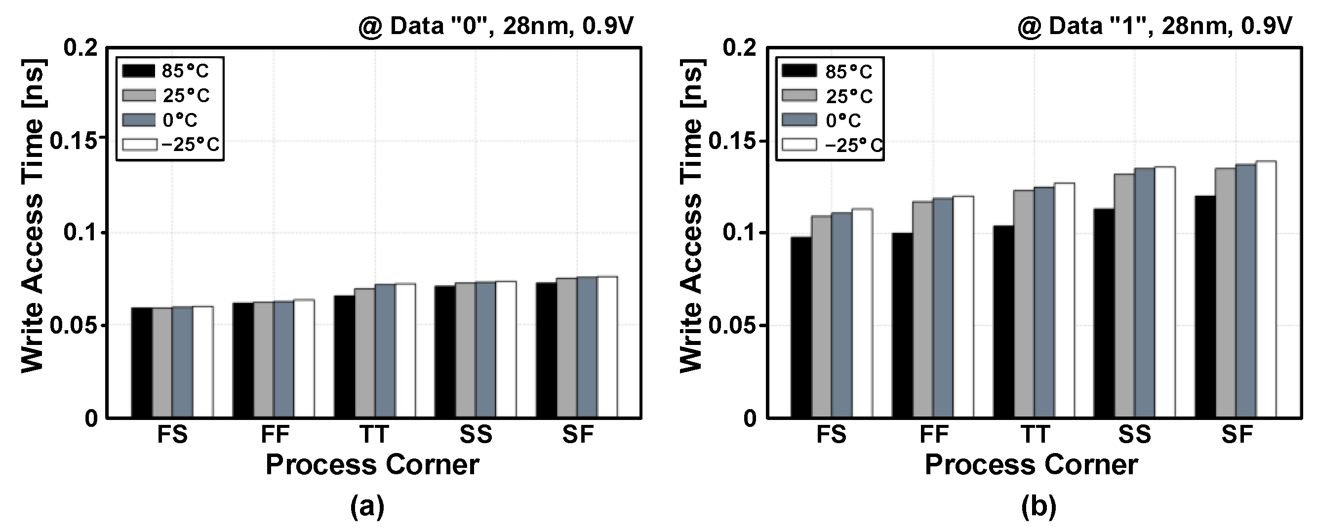
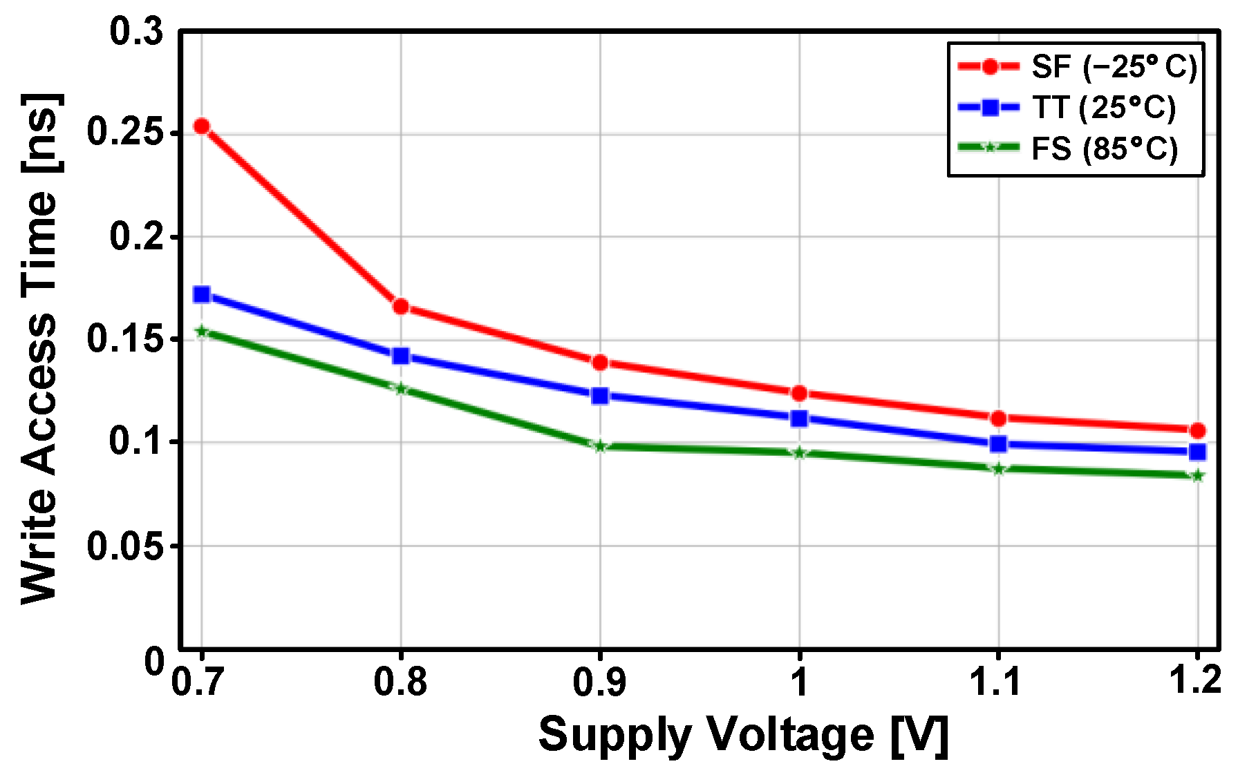
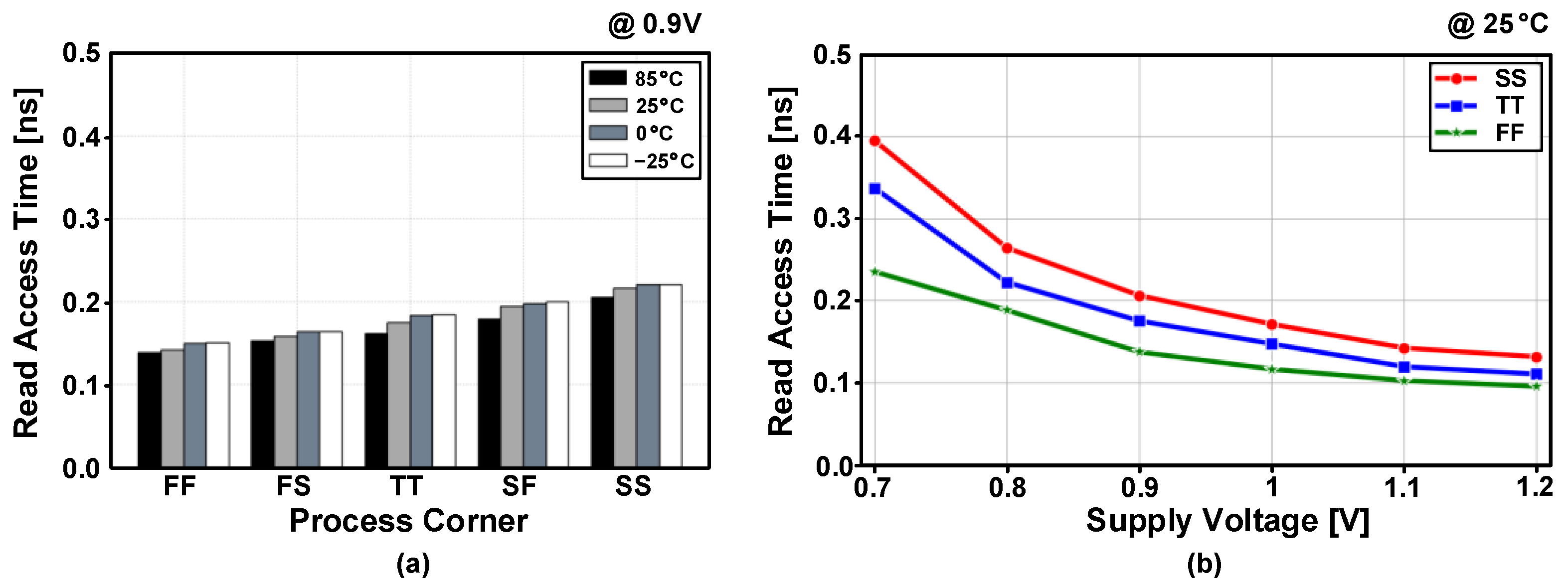
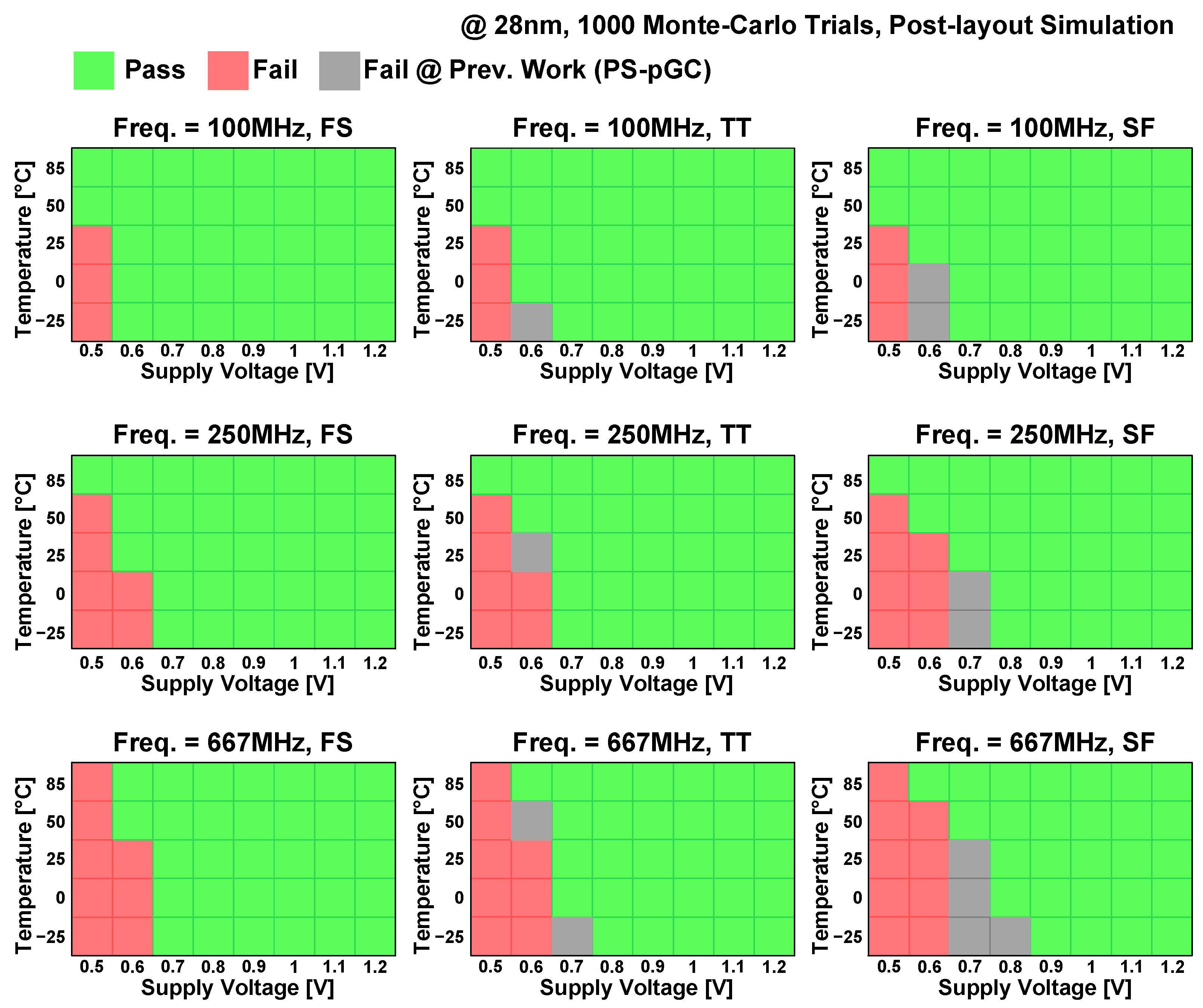
4. Simulation and Experimental Results
5. Comparison between PS-nGC and PS-pGC
6. Conclusions
Author Contributions
Funding
Institutional Review Board Statement
Informed Consent Statement
Data Availability Statement
Conflicts of Interest
References
- Yu, C.; Yoo, T.; Chai, K.T.C.; Kim, T.T.-H.; Kim, B. A 65-nm 8T SRAM Compute-in-Memory Macro with Column ADCs for Processing Neural Networks. IEEE J. Solid-State Circuits 2022, 57, 3466–3476. [Google Scholar] [CrossRef]
- Mu, J.; Kim, H.; Kim, B. SRAM-Based In-Memory Computing Macro Featuring Voltage-Mode Accumulator and Row-by-Row ADC for Processing Neural Networks. IEEE Trans. Circuits Syst. I Regul. Pap. 2022, 69, 2412–2422. [Google Scholar] [CrossRef]
- Yu, C.; Yoo, T.; Kim, T.T.; Tshun Chuan, K.C.; Kim, B. A 16K Current-Based 8T SRAM Compute-In-Memory Macro with Decoupled Read/Write and 1-5bit Column ADC. In Proceedings of the IEEE Custom Integrated Circuits Conference (CICC), Boston, MA, USA, 22–25 March 2020; pp. 1–4. [Google Scholar]
- Kim, S.; Lee, W.; Kim, S.; Park, S.; Jeon, D. An In-Memory Computing SRAM Macro for Memory-Augmented Neural Network. IEEE Trans. Circuits Syst. II Express Briefs 2022, 69, 1687–1691. [Google Scholar] [CrossRef]
- Chae, C.; Kim, S.; Choi, J.; Park, J.-E. A Multi-Bit In-Memory-Computing SRAM Macro Using Column-Wise Charge Redistribution for DNN Inference in Edge Computing Devices. In Proceedings of the 18th International SoC Design Conference (ISOCC), Jeju Island, Republic of Korea, 6–9 October 2021; pp. 421–422. [Google Scholar]
- Jiang, Z.; Yin, S.; Seo, J.; Seok, M. C3SRAM: An In-Memory-Computing SRAM Macro Based on Robust Capacitive Coupling Computing Mechanism. IEEE J. Solid-State Circuits 2020, 55, 1888–1897. [Google Scholar] [CrossRef]
- Wang, L.; Ye, W.; Lai, J.; Liu, J.; Yang, J.; Si, X.; Huo, C.; Dou, C.; Xu, X.; Liu, Q.; et al. A 14nm 100Kb 2T1R Transpose RRAM with >150X resistance ratio enhancement and 27.95% reduction on energy-latency product using low-power near threshold read operation and fast data-line current stabling scheme. In Proceedings of the 2021 Symposium on VLSI Technology, Kyoto, Japan, 13–19 June 2021; pp. 1–2. [Google Scholar]
- Ye, W.; Wang, L.; Zhou, Z.; An, J.; Li, W.; Gao, H.; Li, Z.; Yue, J.; Hu, H.; Xu, X.; et al. A 28-nm RRAM Computing-in-Memory Macro Using Weighted Hybrid 2T1R Cell Array and Reference Subtracting Sense Amplifier for AI Edge Inference. IEEE J. Solid-State Circuits 2023, 58, 2839–2850. [Google Scholar] [CrossRef]
- Chen, W.-H.; Li, K.-X.; Lin, W.-Y.; Hsu, K.-H.; Li, P.-Y.; Yang, C.-H.; Xue, C.-X.; Yang, E.-Y.; Chen, Y.-K.; Chang, Y.-S.; et al. A 65nm 1Mb nonvolatile computing-in-memory ReRAM macro with sub-16ns multiply-and-accumulate for binary DNN AI edge processors. In Proceedings of the IEEE International Solid-State Circuits Conference-(ISSCC), San Francisco, CA, USA, 11–15 February 2018. [Google Scholar]
- Chen, Y.; Lu, L.; Kim, B.; Kim, T.T.-H. Reconfigurable 2T2R ReRAM Architecture for Versatile Data Storage and Computing In-Memory. IEEE Trans. Very Large Scale Integr. VLSI Syst. 2020, 28, 2636–2649. [Google Scholar] [CrossRef]
- Chen, Y.; Lu, L.; Kim, B.; Kim, T.T.-H. A Reconfigurable 4T2R ReRAM Computing In-Memory Macro for Efficient Edge Applications. IEEE Open J. Circuits Syst. 2021, 2, 210–222. [Google Scholar] [CrossRef]
- Khwa, W.-S.; Chiu, Y.-C.; Jhang, C.-J.; Huang, S.-P.; Lee, C.-Y.; Wen, T.-H.; Chang, F.-C.; Yu, S.-M.; Lee, T.-Y.; Chang, M.-F. A 40-nm, 2M-Cell, 8b-Precision, Hybrid SLC-MLC PCM Computing-in-Memory Macro with 20.5-65.0TOPS/W for Tiny-Al Edge Devices. In Proceedings of the IEEE International Solid-State Circuits Conference-(ISSCC), San Francisco, CA, USA, 20–26 February 2022; pp. 1–3. [Google Scholar]
- Chiu, Y.-C.; Yang, C.-S.; Teng, S.-H.; Huang, H.-Y.; Chang, F.-C.; Wu, T.; Chien, Y.-A.; Hsieh, F.-L.; Li, C.-Y.; Lin, G.-Y.; et al. A 22nm 4Mb STT-MRAM Data-Encrypted Near-Memory Computation Macro with a 192GB/s Read-and-Decryption Bandwidth and 25.1-55.1TOPS/W 8b MAC for AI Operations. In Proceedings of the 2022 IEEE International Solid-State Circuits Conference (ISSCC), San Francisco, CA, USA, 18–22 February 2022; pp. 178–180. [Google Scholar]
- Roy, S.K.; Ou, H.-M.; Ahmed, M.G.; Deaville, P.; Zhang, B.; Verma, N.; Hanumolu, P.K.; Changbhag, N.R. Compute SNR-boosted 22 nm MRAM-based In-memory Computing Macro using Statistical Error Compensation. In Proceedings of the ESSCIRC 2023-IEEE 49th European Solid State Circuits Conference (ESSCIRC), Lisbon, Portugal, 11–14 September 2023; pp. 25–28. [Google Scholar]
- Chiu, Y.-C.; Khwa, W.-S.; Li, C.-Y.; Hsieh, F.-L.; Chien, Y.-A.; Lin, G.-Y.; Chen, P.-J.; Pan, T.-H.; You, D.-Q.; Chen, F.-Y.; et al. A 22nm 8Mb STT-MRAM Near-Memory-Computing Macro with 8b-Precision and 46.4-160.1TOPS/W for Edge-AI Devices. In Proceedings of the 2023 IEEE International Solid-State Circuits Conference (ISSCC), San Francisco, CA, USA, 19–23 February 2023; pp. 496–498. [Google Scholar]
- Raman, S.R.S.; Xie, S.; Kulkarni, J.P. Compute-in-eDRAM with Backend Integrated Indium Gallium Zinc Oxide Transistors. In Proceedings of the IEEE International Symposium on Circuits and Systems (ISCAS), Daegu, Republic of Korea, 22–28 May 2021; pp. 1–5. [Google Scholar]
- Ha, S.; Kim, S.; Han, D.; Um, S.; Yoo, H.J. A 36.2 dB High SNR and PVT/Leakage-robust eDRAM Computing-In-Memory Macro with Segmented BL and Reference Cell Array. IEEE Trans. Circuits Syst. II Express Briefs 2022, 69, 2433–2437. [Google Scholar] [CrossRef]
- Yu, C.; Yoo, T.; Kim, H.; Kim, T.T.-H.; Chuan, K.C.T.; Kim, B. A Logic-Compatible eDRAM Compute-In-Memory with Embedded ADCs for Processing Neural Networks. IEEE Trans. Circuits Syst. I Regul. Pap. 2021, 68, 667–679. [Google Scholar] [CrossRef]
- Xie, S.; Ni, C.; Sayal, A.; Jain, P.; Hamzaoglu, F.; Kulkarni, J.P. 16.2 eDRAM-CIM: Compute-In-Memory Design with Reconfigurable Embedded-Dynamic-Memory Array Realizing Adaptive Data Converters and Charge-Domain Computing. In Proceedings of the IEEE International Solid-State Circuits Conference (ISSCC), San Francisco, CA, USA, 13–22 February 2021. [Google Scholar]
- Kim, D.; Yum, C.; Xie, S.; Chen, Y.; Kim, J.-Y.; Kim, B.; Kilkarni, J.-P.; Kim, T.T.-H. An Overview of Processing-in-Memory Circuits for Artificial Intelligence and Machine Learning. IEEE J. Emerg. Sel. Top. Circuits Syst. 2022, 12, 338–353. [Google Scholar] [CrossRef]
- Golman, R.; Giterman, R.; Teman, A. Configurable Multi-Port Dynamic Bitcell with Internal Refresh Mechanism. In Proceedings of the IEEE International Conference on Electronics, Circuits and Systems (ICECS), Bordeaux, France, 9–12 December 2018; pp. 589–592. [Google Scholar]
- Maltabashi, O.; Marinberg, H.; Giterman, R.; Teman, A. A 5-Transistor Ternary Gain-Cell eDRAM with Parallel Sensing. In Proceedings of the IEEE International Symposium on Circuits and Systems (ISCAS), Florence, Italy, 27–30 May 2018; pp. 1–5. [Google Scholar]
- Edri, N.; Meinerzhagen, P.; Teman, A.; Burg, A.; Fish, A. Silicon-Proven, Per-Cell Retention Time Distribution Model for Gain-Cell Based eDRAMs. IEEE Trans. Circuits Syst. I Regul. Pap. 2016, 63, 222–232. [Google Scholar] [CrossRef]
- Zhang, W.; Chun, K.C.; Kim, C.H. A Write-Back-Free 2T1D Embedded DRAM With Local Voltage Sensing and a Dual-Row-Access Low Power Mode. IEEE Trans. Circuits Syst. I Regul. Pap. 2013, 60, 2030–2038. [Google Scholar] [CrossRef]
- Chun, K.C.; Zhang, W.; Jain, P.; Kim, C.H. A 700MHz 2T1C embedded DRAM macro in a generic logic process with no boosted supplies. In Proceedings of the 2011 IEEE International Solid-State Circuits Conference, San Francisco, CA, USA, 20–24 February 2011; pp. 506–507. [Google Scholar]
- Huang, K.C.; Ting, Y.W.; Chang, C.Y.; Tu, K.C.; Tzeng, K.C.; Chu, H.C.; Pai, C.Y.; Katoch, A.; Kuo, W.H.; Chen, K.W.; et al. A high-performance, high-density 28nm eDRAM technology with high-K/metal-gate. In Proceedings of the 2011 International Electron Devices Meeting, Washington, DC, USA, 5–7 December 2011; pp. 24.7.1–24.7.4. [Google Scholar]
- Liu, J.; Sun, C.; Tang, W.; Zheng, Z.; Liu, Y.; Yang, H.; Jiang, C.; Ni, K.; Gong, X.; Li, X.; et al. Low-Power and Scalable Retention-Enhanced IGZO TFT eDRAM-Based Charge-Domain Computing. In Proceedings of the 2021 IEEE International Electron Devices Meeting (IEDM), San Francisco, CA, USA, 11–15 December 2021; pp. 21.1.1–21.1.4. [Google Scholar]
- Kim, S.; Park, J.-E. Pseudo-Static Gain Cell of Embedded DRAM for Processing-in-Memory in Intelligent IoT Sensor Nodes. Sensors 2022, 22, 4284. [Google Scholar] [CrossRef]
- Chun, K.C.; Jain, P.; Kim, T.; Kim, C.H. A 667 MHz Logic-Compatible Embedded DRAM Featuring an Asymmetric 2T Gain Cell for High Speed On-Die Caches. IEEE J. Solid-State Circuits 2012, 47, 547–559. [Google Scholar] [CrossRef]
- Somasekhar, D.; Ye, Y.; Aseron, P.; Lu, S.-L.; Khellah, M.M.; Howard, J.; Ruhl, G.; Karnik, T.; Borkar, S.; De, Y.K.; et al. 2 GHz 2 Mb 2T Gain Cell Memory Macro With 128 GBytes/sec Bandwidth in a 65 nm Logic Process Technology. IEEE J. Solid-State Circuits 2009, 44, 174–185. [Google Scholar] [CrossRef]
- Garzón, E.; Greenblatt, Y.; Harel, O.; Lanuzza, M.; Teman, A. Gain-Cell Embedded DRAM Under Cryogenic Operation—A First Study. IEEE Trans. Very Large Scale Integr. VLSI Syst. 2021, 29, 1319–1324. [Google Scholar] [CrossRef]
- Giterman, R.; Fish, A.; Burg, A.; Teman, A. A 4-Transistor nMOS-Only Logic-Compatible Gain-Cell Embedded DRAM With Over 1.6-ms Retention Time at 700 mV in 28-nm FD-SOI. IEEE Trans. Circuits Syst. I Regul. Pap. 2018, 65, 1245–1256. [Google Scholar] [CrossRef]
- Giterman, R.; Fish, A.; Geuli, N.; Mentovich, E.; Burg, A.; Teman, A. An 800-MHz Mixed-VT 4T IFGC Embedded DRAM in 28-nm CMOS Bulk Process for Approximate Storage Applications. IEEE J. Solid-State Circuits 2018, 53, 2136–2148. [Google Scholar] [CrossRef]
- Zhang, K.; Bhattacharya, U.; Chen, Z.; Hamzaoglu, F.; Murray, D.; Vallepalli, N.; Wang, Y.; Bohr, B.Z.M. SRAM design on 65-nm CMOS technology with dynamic sleep transistor for leakage reduction. IEEE J. Solid-State Circuits 2005, 40, 895–901. [Google Scholar] [CrossRef]
- Chang, L.; Montoye, R.K.; Nakamura, Y.; Baston, K.A.; Eickemeyer, R.J.; Dennard, R.H.; Haensch, W.; Jamesek, D. An 8T-SRAM for Variability Tolerance and Low-Voltage Operation in High-Performance Caches. IEEE J. Solid-State Circuits 2008, 43, 956–963. [Google Scholar] [CrossRef]
- Chun, K.C.; Jain, P.; Lee, J.H.; Kim, C.H. A 3T Gain Cell Embedded DRAM Utilizing Preferential Boosting for High Density and Low Power On-Die Caches. IEEE J. Solid-State Circuits 2011, 46, 1495–1505. [Google Scholar] [CrossRef]
- Meinerzhagen, P.; Teman, A.; Giterman, R.; Edri, N.; Burg, A.; Fish, A. Gain-Cell Embedded DRAMs for Low-Power VLSI Systems-on-Chip; Springer: Basel, Switzerland, 2018. [Google Scholar]
- Giterman, R.; Teman, A.; Meinerzhagen, P.; Atias, L.; Burg, A.; Fish, A. Single-Supply 3T Gain-Cell for Low-Voltage Low-Power Applications. IEEE Trans. Very Large Scale Integr. VLSI Syst. 2016, 24, 358–362. [Google Scholar] [CrossRef]
- Hwang, M.-E.; Kwon, S. A 0.94 μW 611 KHz In-Situ Logic Operation in Embedded DRAM Memory Arrays in 90 nm CMOS. Electronics 2019, 8, 865. [Google Scholar] [CrossRef]
- Samizadeh Nikoo, M.; Jafari, A.; Perera, N.; Zhu, M.; Santoruvo, G.; Matioli, E. Nanoplasma-enabled picosecond switches for ultrafast electronics. Nature 2020, 579, 534–539. [Google Scholar] [CrossRef]
- Mohammad, T.; Wenshan, C. All-Optical Control of Light in Micro- and Nanophotonics. ACS Photonics 2019, 6, 1082–1093. [Google Scholar]


| 2T [29] | 2T [30] | 3T [36] | 3T [24] | 4T [32] | PS-pGC [28] | This Work | |||
|---|---|---|---|---|---|---|---|---|---|
| Bitcell Schematic |  |  |  |  |  |  |  | ||
| Process | 65 nm | 65 nm LP | 65 nm LP | 65 nm LP | 28 nm FD-SOI | 28 nm | 28 nm | ||
| Bitcell Area | 0.275 μm2 | 0.478 μm2 | 0.627 μm2 | 0.674 μm2 | 0.23 μm2 | 0.286 μm2 | 0.284 μm2 | ||
| Bitcell Area Normalized to 28 nm Process | 0.075 μm2 | 0.13 μm2 | 0.21 μm2 | 0.26 μm2 | 0.23 μm2 | 0.286 μm2 | 0.284 μm2 | ||
| Retention Time | 10 μs @ 85 °C | 276.5 μs @ 85 °C | 1.25 ms @ 85 °C | 325 μs @ 85 °C | 154 μs @ 85 °C | Static | Static | ||
| Maximum Freq. | 2 GHz | 667 MHz | NA | 1 GHz | 66 MHz | 100 MHz | 667 MHz | 100 MHz | 667 MHz |
| VDD Range | 0.7–1.1 V | 0.8–1.4 V | 0.8–1.3 V | 0.8–1.2 V | 0.6–0.9 V | 0.7–1.2 V | 0.9–1.2 V | 0.6–1.2 V | 0.7–1.2 V |
| Temp. Range | 25–85 °C | 25–85 °C | 25–85 °C | 25–85 °C | 0–85 °C | −25–85 °C | −25–85 °C | ||
| Write Access Time | NA | 0.21 ns @ 85 °C | 0.27 ns @ 85 °C | 1.5 ns @ 85 °C | 0.46–0.67 ns @ 27 °C | 0.34 ns @ 85 °C, TT | 0.104 ns @ 85 °C, TT | ||
| Read Access Time | NA | 0.46 ns @ 85 °C | 0.61 ns @ 85 °C | 1 ns @ 85 °C | <3 ns @ 27 °C | 0.29 ns @ 85 °C, TT | 0.16 ns @ 85 °C, TT | ||
| Additional Bit/Wordline? | No | No | No | Yes | No | No | No | ||
| Need Refresh? | Yes | Yes | Yes | Yes | Yes | No | No | ||
| Retention Power | 508 mW/2 Mb @ 85 °C | 1.16 mW/Mb @ 85 °C | 1.25 mW/Mb @ 85 °C | NA | 909 nW/8 kb @ 85 °C | 22.5 μW/4 kb @ 85 °C, TT | 25.4 μW/4 kb @ 85 °C, TT | ||
Disclaimer/Publisher’s Note: The statements, opinions and data contained in all publications are solely those of the individual author(s) and contributor(s) and not of MDPI and/or the editor(s). MDPI and/or the editor(s) disclaim responsibility for any injury to people or property resulting from any ideas, methods, instructions or products referred to in the content. |
© 2023 by the authors. Licensee MDPI, Basel, Switzerland. This article is an open access article distributed under the terms and conditions of the Creative Commons Attribution (CC BY) license (https://creativecommons.org/licenses/by/4.0/).
Share and Cite
Kim, S.; Jeong, I.; Park, J.-E. An N-Type Pseudo-Static eDRAM Macro with Reduced Access Time for High-Speed Processing-in-Memory in Intelligent Sensor Hub Applications. Sensors 2023, 23, 9329. https://doi.org/10.3390/s23239329
Kim S, Jeong I, Park J-E. An N-Type Pseudo-Static eDRAM Macro with Reduced Access Time for High-Speed Processing-in-Memory in Intelligent Sensor Hub Applications. Sensors. 2023; 23(23):9329. https://doi.org/10.3390/s23239329
Chicago/Turabian StyleKim, Subin, Ingu Jeong, and Jun-Eun Park. 2023. "An N-Type Pseudo-Static eDRAM Macro with Reduced Access Time for High-Speed Processing-in-Memory in Intelligent Sensor Hub Applications" Sensors 23, no. 23: 9329. https://doi.org/10.3390/s23239329
APA StyleKim, S., Jeong, I., & Park, J.-E. (2023). An N-Type Pseudo-Static eDRAM Macro with Reduced Access Time for High-Speed Processing-in-Memory in Intelligent Sensor Hub Applications. Sensors, 23(23), 9329. https://doi.org/10.3390/s23239329